Assignment
- group assignment
- probe an input device's analog levels and digital signals
- individual assignment
- measure something: add a sensor to a microcontroller board that you have designed and read it
Disclaimer
I missed this week's assignment during the semester. The content below is retrofitted from my Week 12 assignment, which was documented first. The Week 12 project involved building a PS/2 numpad input device that communicates over I2C — this post extracts the input device portion of that work.
What to make
For my final project I will have multiple secondary MCUs that talk to the main MCU. For this assignment, I want to build a board that connects to a PS/2 device and reads keystroke input. The input device is a vintage Dell numpad that uses the PS/2 protocol.
Research
I started by searching for a past project that uses a PS/2 device and interprets the data with an Arduino board. djsadeepa posted one such project on Instructables.
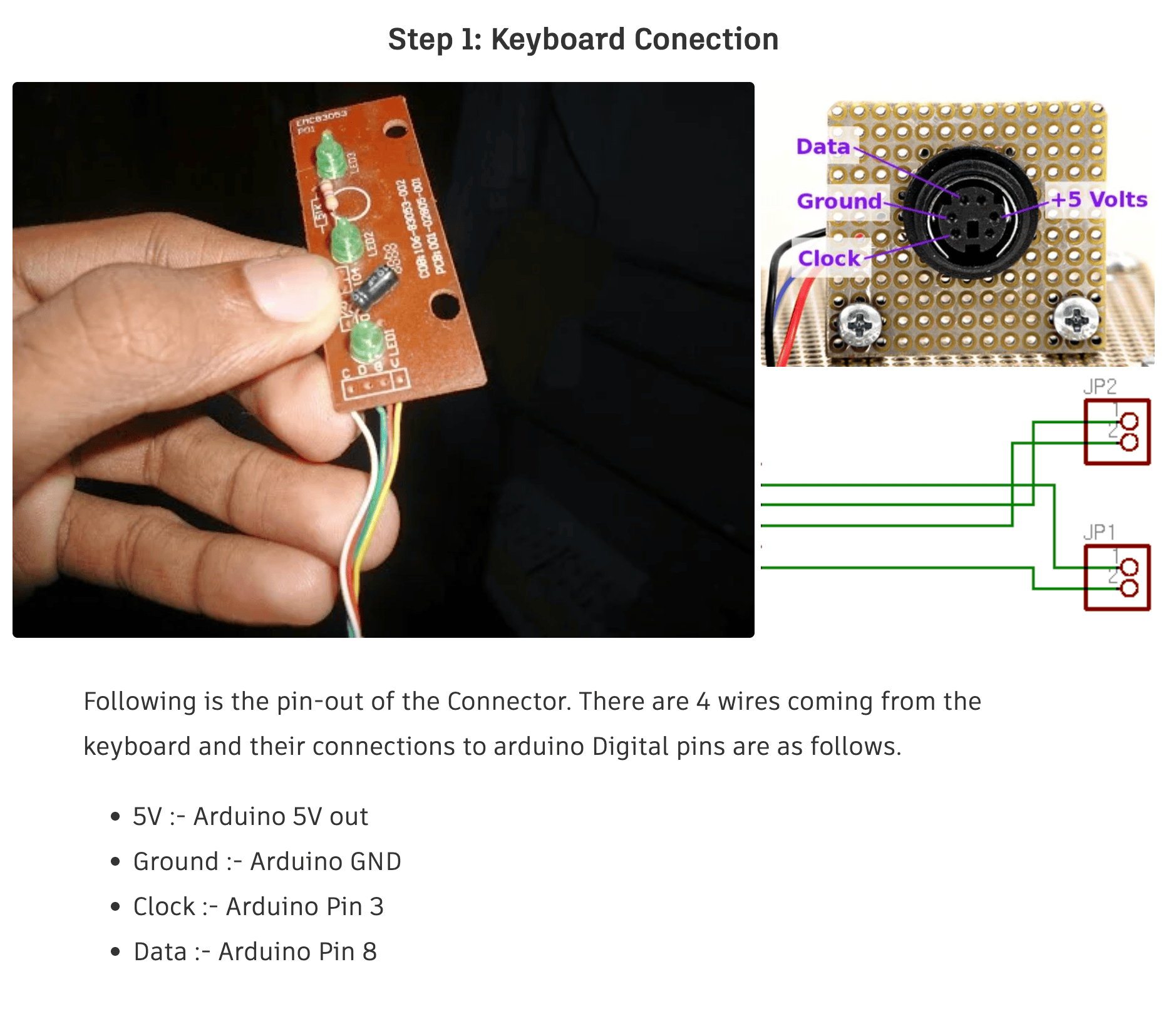
It turns out that for a PS/2 device using the mini DIN 6-pin connector, there are only 4 pins that are used for data transmission: CLK, DATA, +5V, and GND. All I need to do is to connect the CLK and DATA pins to the microcontroller and the rest will happen in software.
PS/2 Port
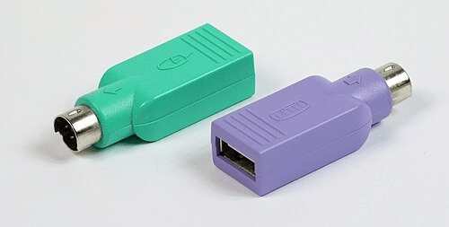
I read a bit more into the PS/2 protocol on Wikipedia. I was always fascinated by the "interoperability" of the PS/2 protocol with USB, remembering these passive USB adapters. I always thought it's a backward compatibility feature from USB, but turns out to be that the I/O device would have to support both protocols, and the adapter only swap the wires to make it fit.
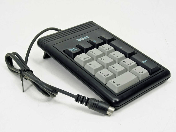
I bought a cute little PS/2 numpad from ebay, a Dell 86004 External Keypad PS/2 17 Key Numpad. It's hard to find a PS/2 numpad online, and this looks quite vintage. I'm not sure which year it was made.
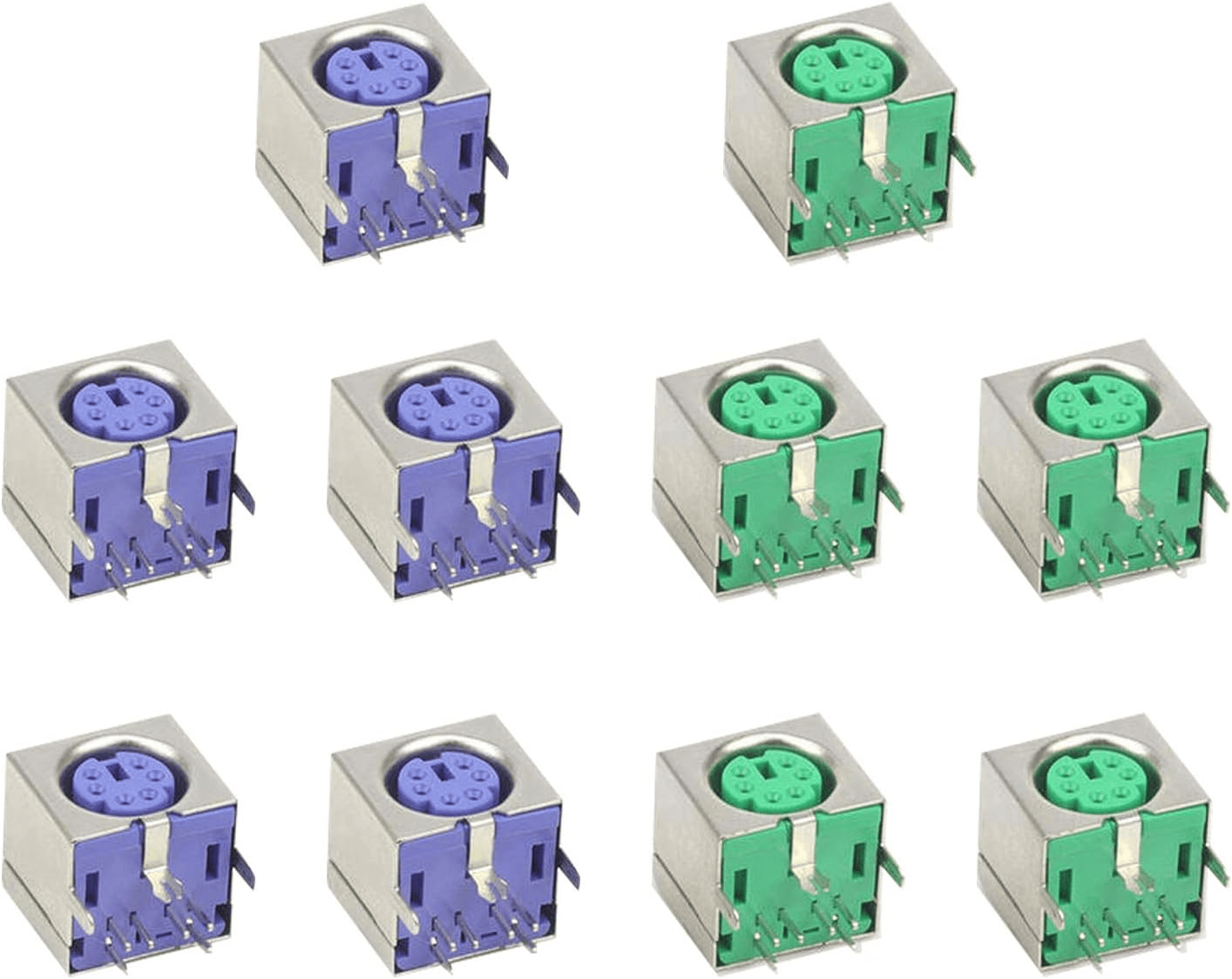
To connect the numpad to the microcontroller, I bought a connector on Amazon to connect the numpad to the PCB.
PS/2 Input Board
The input board has:
- a microcontroller (XIAO ESP32 C3)
- a PS/2 port (to connect to the numpad)
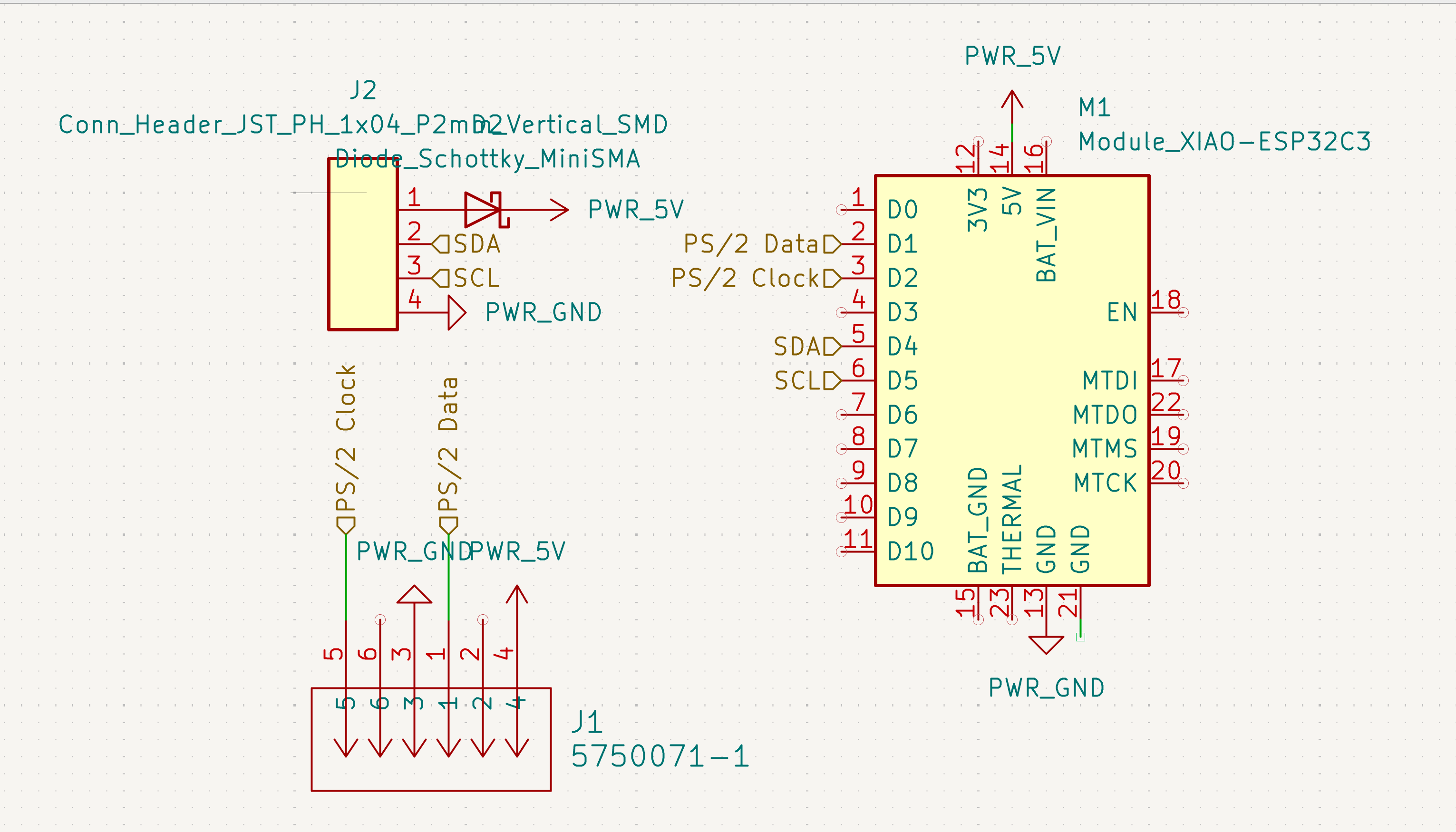
- a JST-XH 2.54mm pitch 4-pin connector (for future I2C communication — see Week 12)
Symbols & Footprints for PS/2 Port
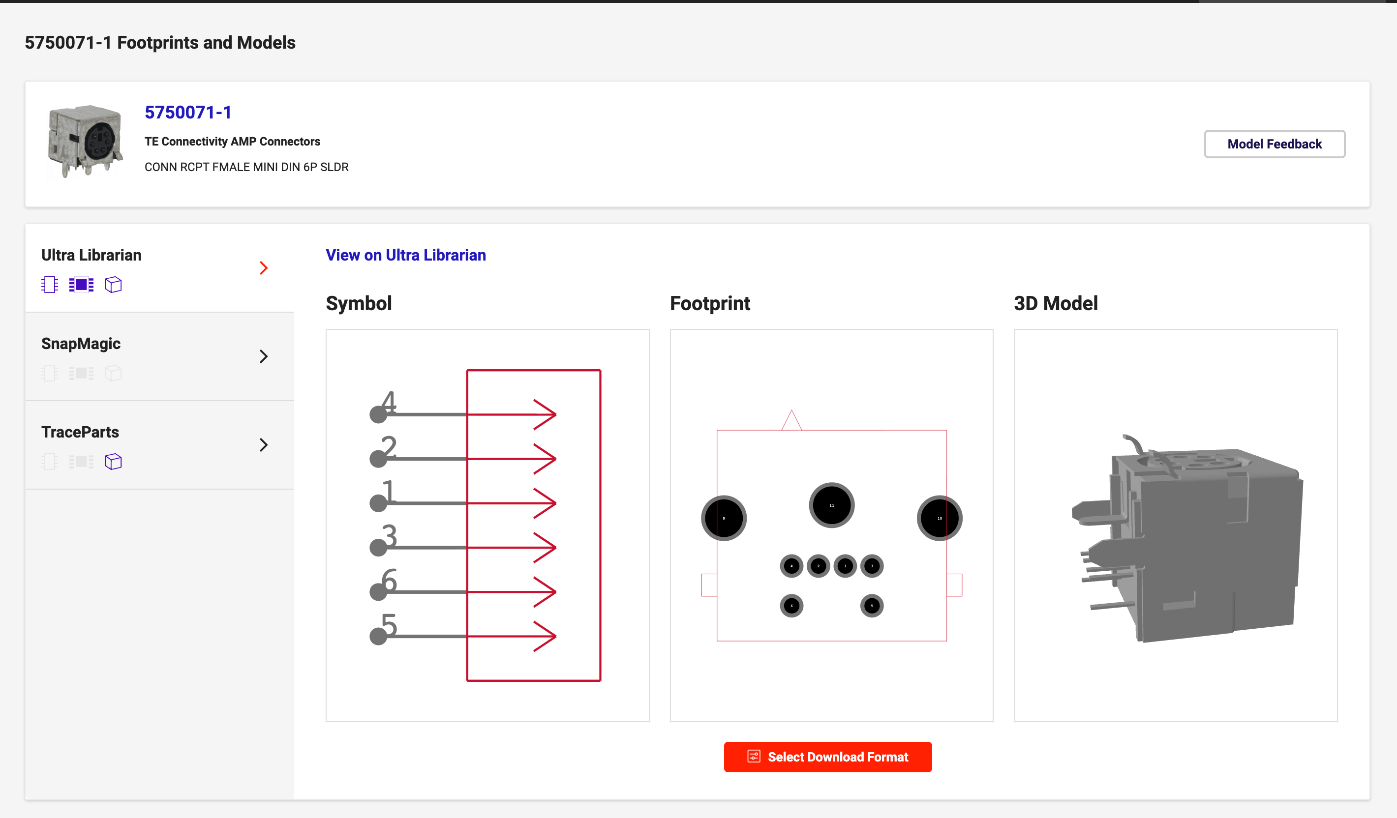
Searching for mini-DIN 6-pin connector, I couldn't find a symbol for my noname amazon connector. The closest I found is 5750071-1 from TE Connectivity AMP Connectors. I assumed it's the same as the connector I bought since it's industry standard (I've seen plenty of them on motherboards and other devices).
Symbols & Footprints for JST-XH Connector
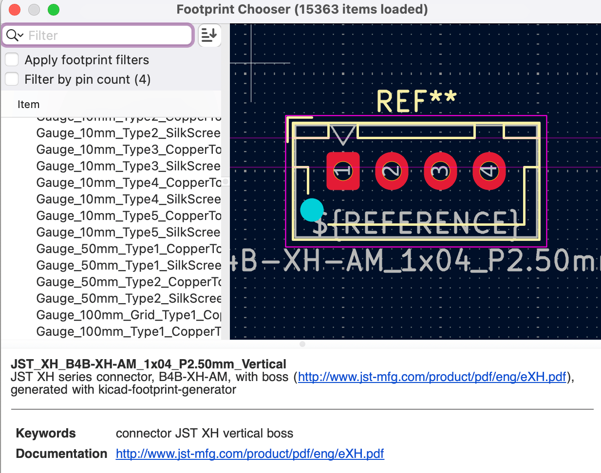
Although the HTMAA inventory includes symbols for JST connectors, the associated footprints did not match my XH series connector. I located the correct footprint in KiCad's connector library: Connector_JST:JST_XH_B4B-XH-AM_1x04_P2.50mm_Vertical.
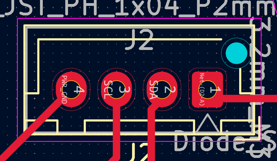
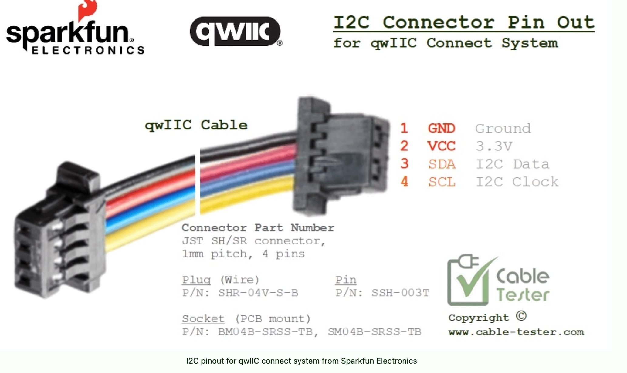
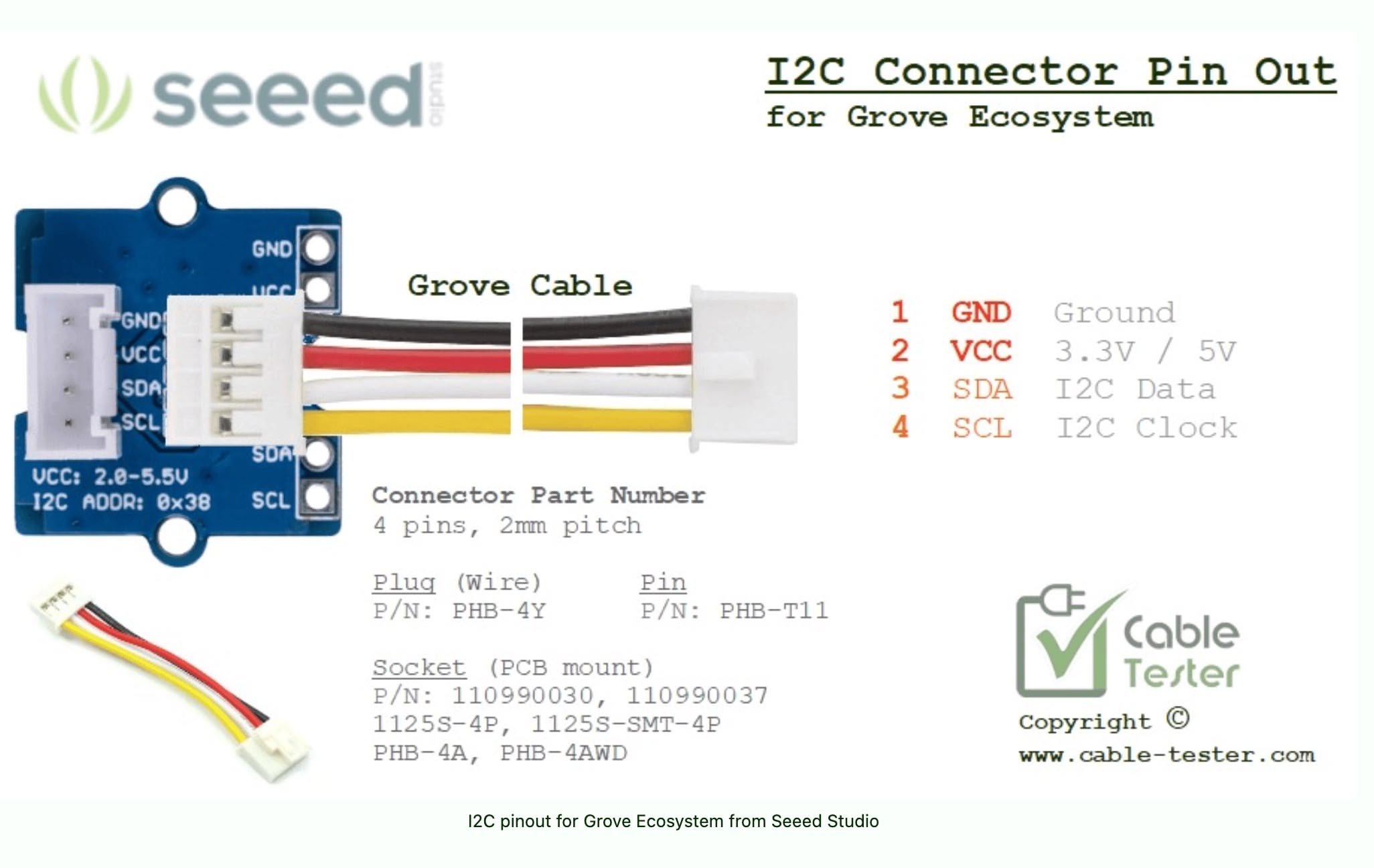
I used this 4-pin connector for I2C communication. One key difference in my design is the use of 5V power instead of the typical 3.3V, as the numpad requires 5V. My custom pinout configuration is VCC, SDA, SCL, and GND. Initially, I thought placing power and ground on opposite ends was a good practice for isolation. However, I later discovered that established ecosystems like Seeed's Grove and SparkFun's Qwiic place power and ground pins adjacent to each other.
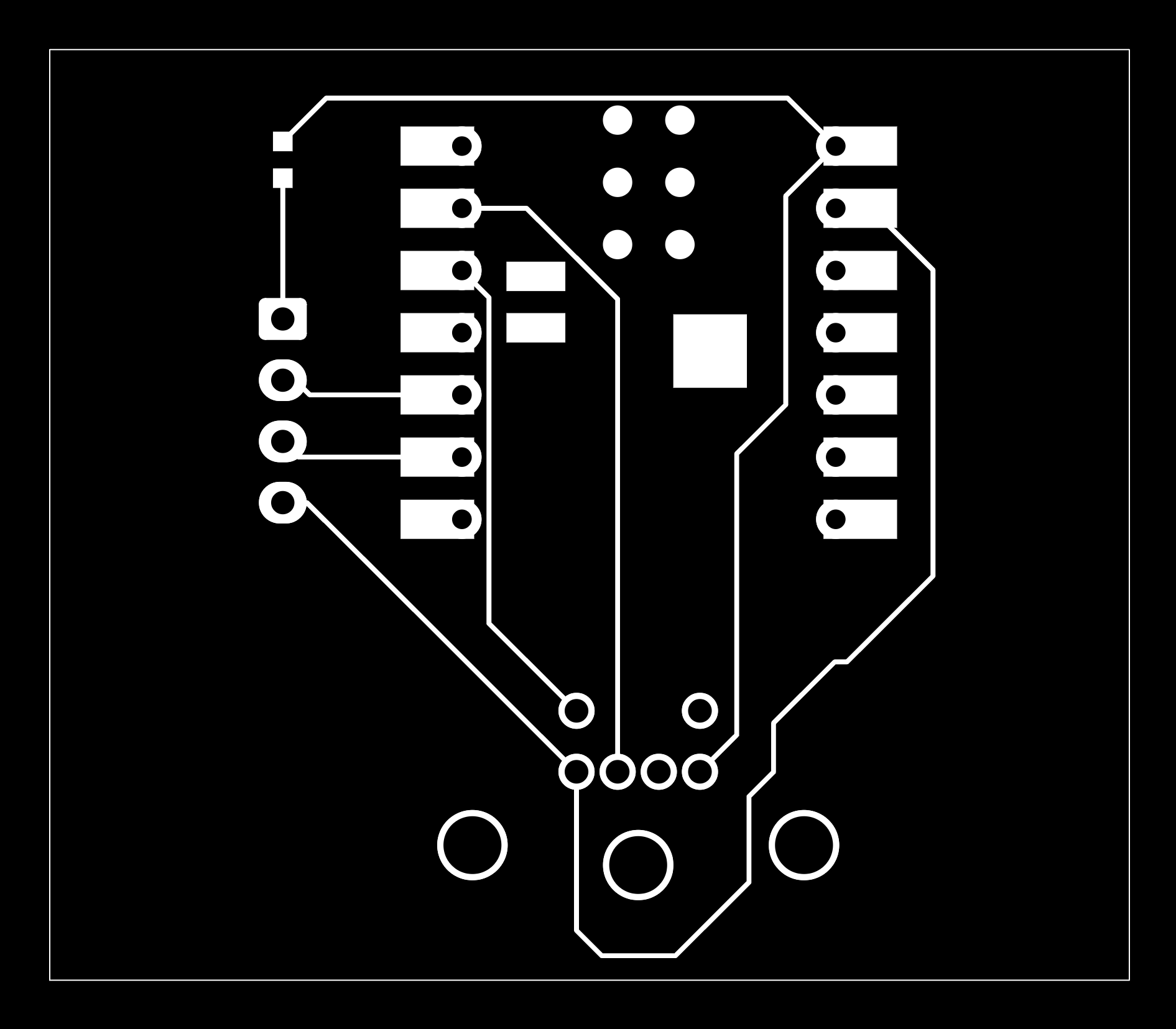
Schematics and PCB
The schematic design is quite straightforward. I assigned GPIO 6 and GPIO 7 for SDA and SCL communication, respectively. I used GPIO 3 for PS/2 Data and GPIO 4 for PS/2 Clock.
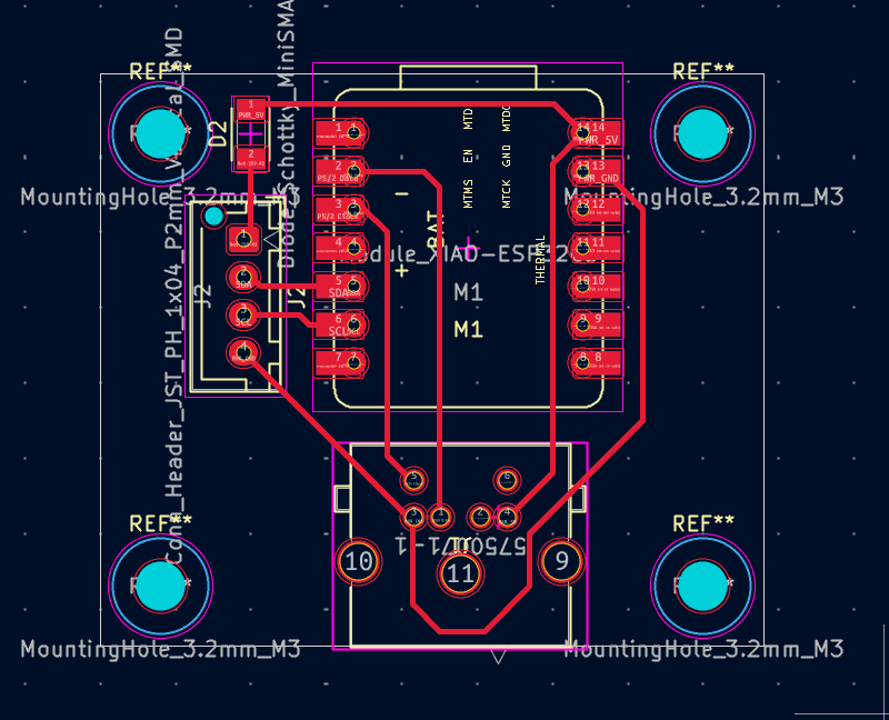
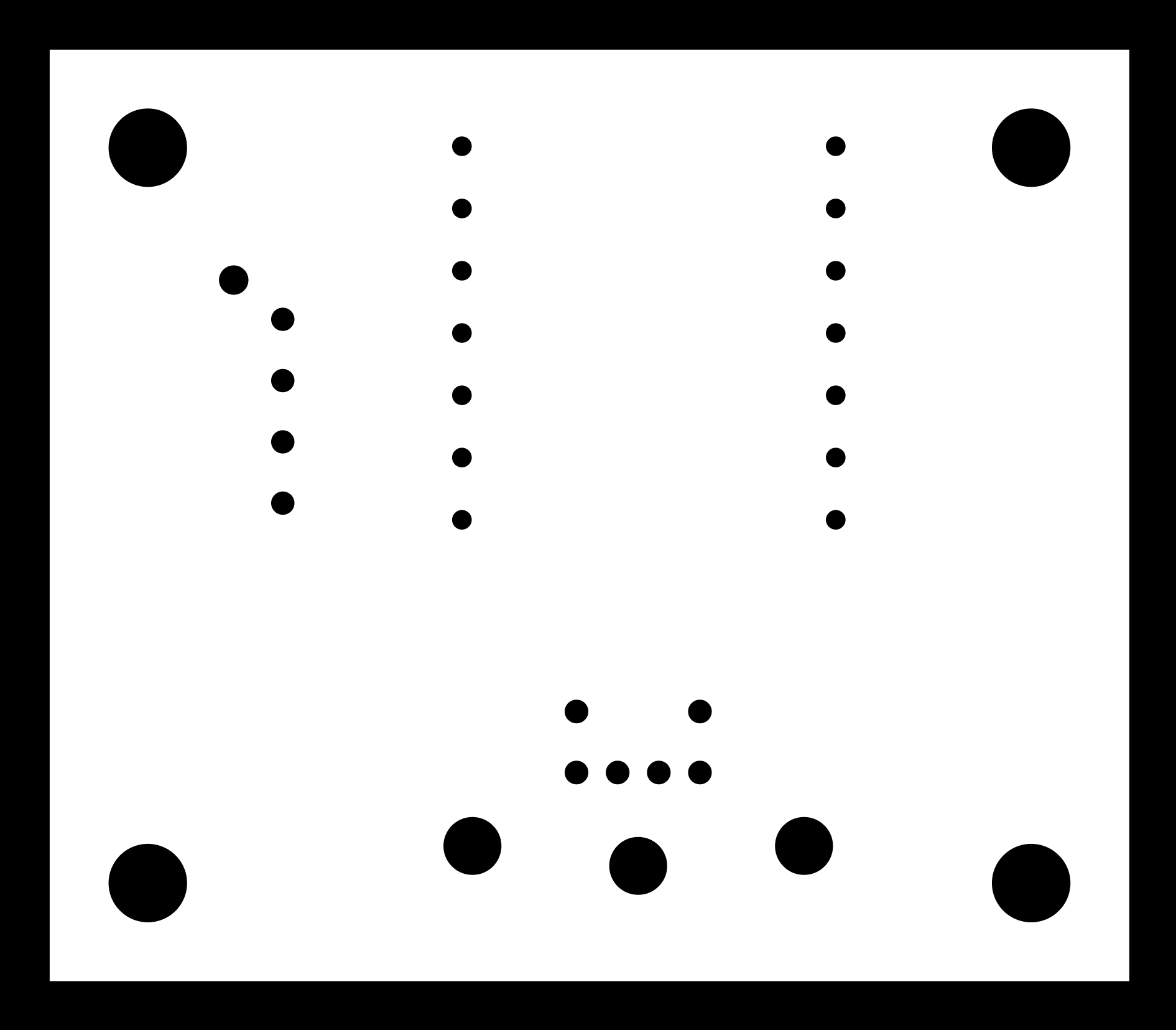
The PCB layout is straightforward. I included four M3 mounting holes at the corners to facilitate easy installation. The routing prioritizes direct connections between the connector and the microcontroller, keeping the board compact and functional.
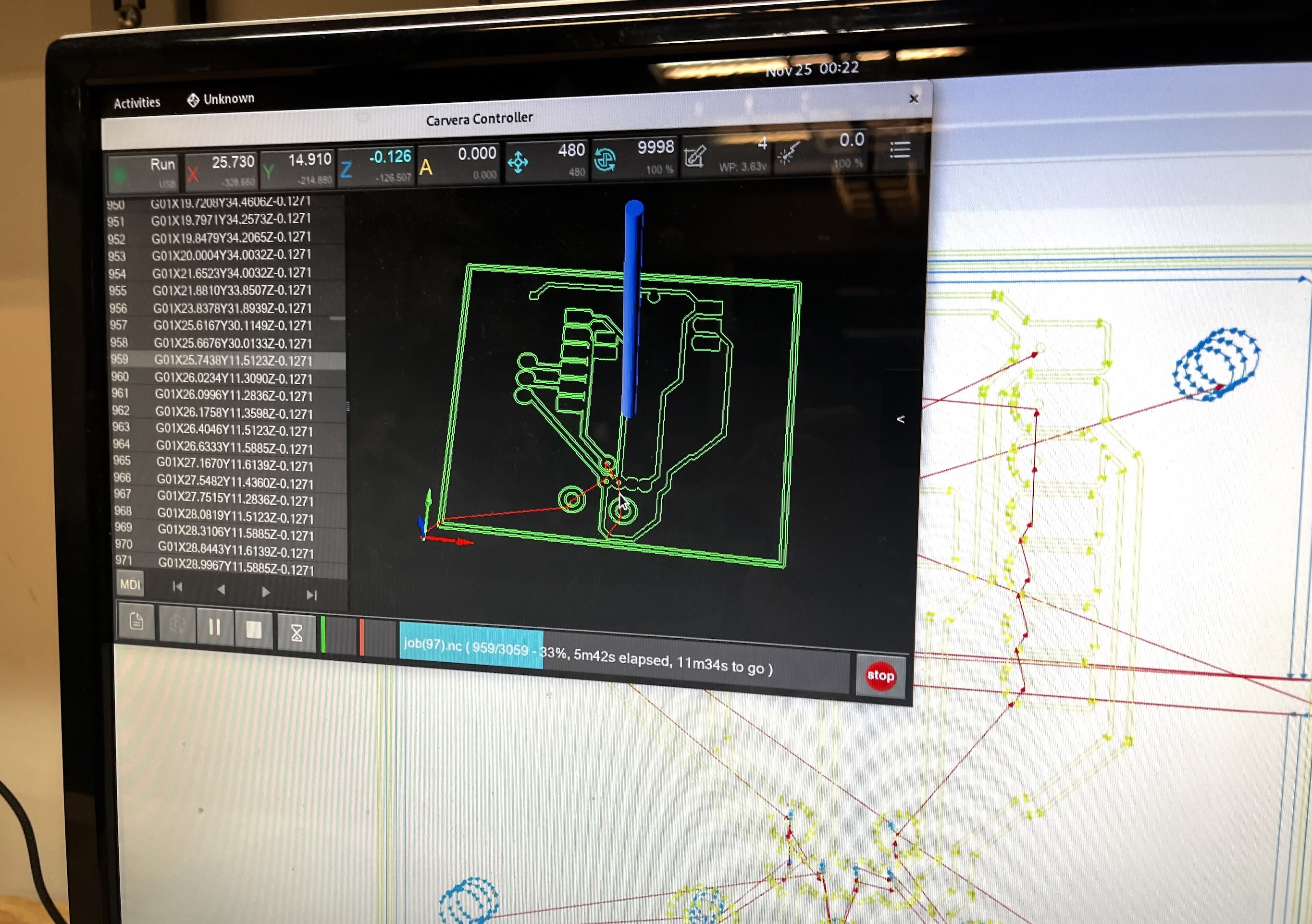
Milling the PCB
To mill the PCB, I utilized the black and white images generated from the Gerber files using Gerber2Img, a tool made by Quentin Bolsée and Jake Read at the MIT Center for Bits and Atoms (2023). I then generated the toolpaths for the Carvera machine using Mods, a browser-based CAM tool.
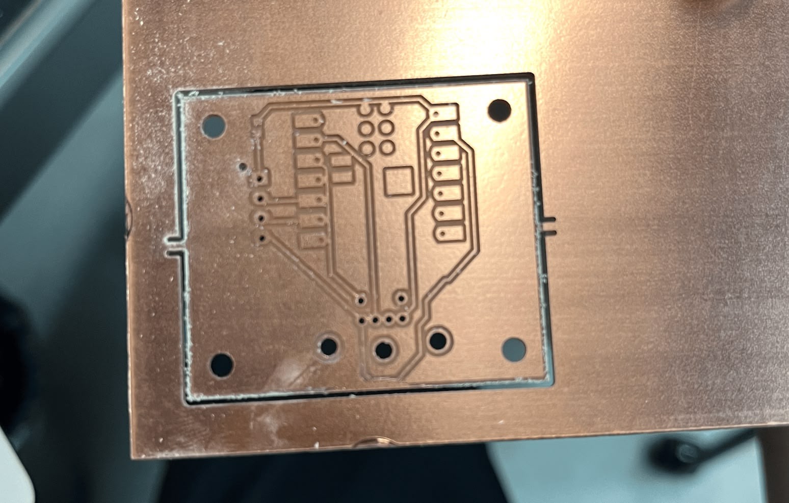
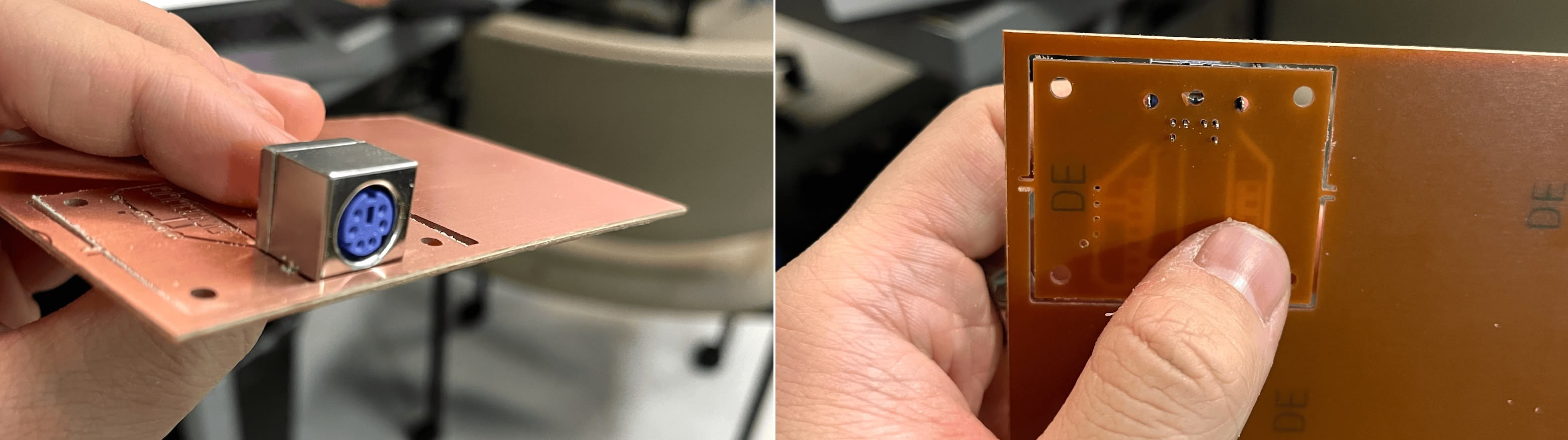
Here is the milled PCB, fresh off the machine.
I did a test fitting with the PS/2 connector before soldering to ensure everything fits correctly.
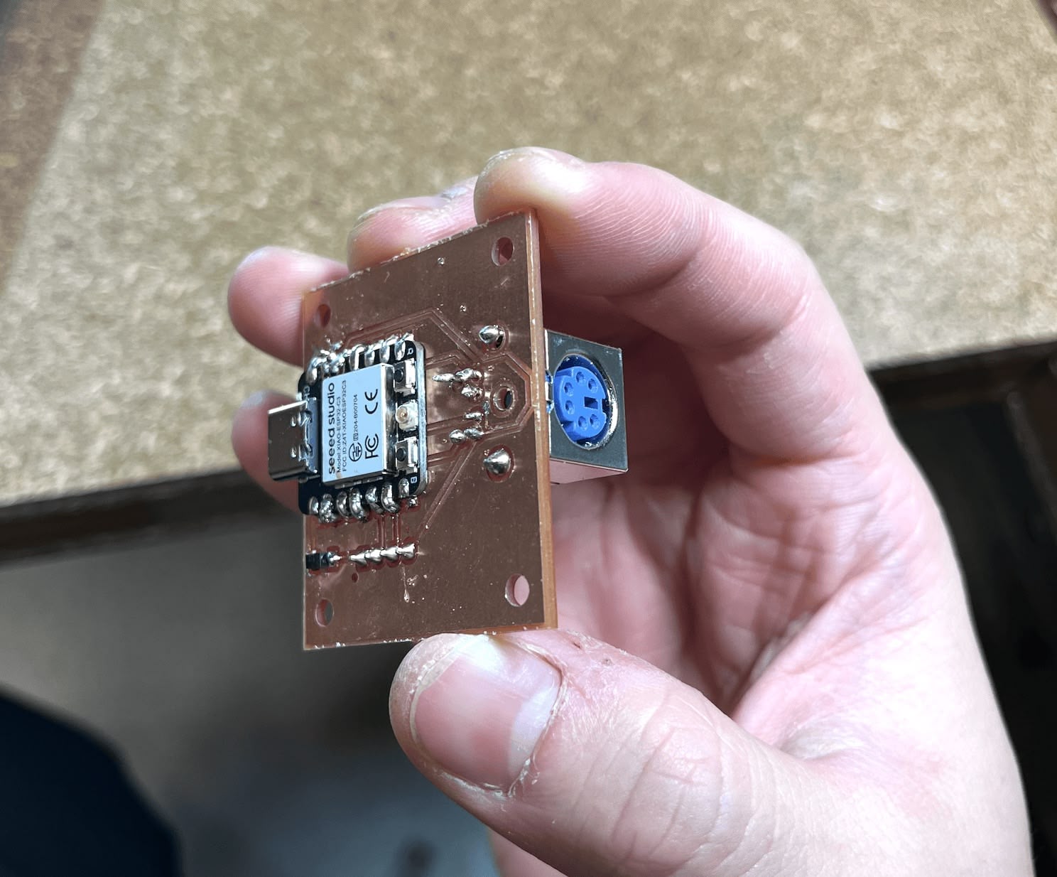
Soldering the PCB
After soldering the components, including the XIAO ESP32 C3, the JST connector, and the PS/2 port, the board was ready.
Software
I used the PS2KeyAdvanced.h library developed by techpaul to read the PS/2 keyboard input.
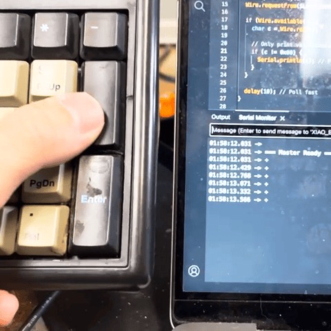
As seen in the video, the serial output displays hex codes (starting with 0x) which represent both press and release events. Most keys worked, though the '5' key was unresponsive. Despite this glitch, I proceeded with the implementation. I added a switch case in the code to map these hex codes back to their corresponding ASCII characters.
The PS/2 Data pin is connected to GPIO 3, and the Clock pin to GPIO 4.
#include <PS2KeyAdvanced.h>

#define PS2_DATA_PIN 3
#define PS2_CLK_PIN 4

PS2KeyAdvanced keyboard;

void setup()
{
  Serial.begin(115200);
  keyboard.begin(PS2_DATA_PIN, PS2_CLK_PIN);
  Serial.println("=== PS/2 Input Device Ready ===");
}

void loop()
{
  if (keyboard.available())
  {
    uint16_t code = keyboard.read();

    // DEBUG: Print the raw code to see what's happening
    Serial.printf("Raw code: 0x%04X\n", code);

    // Ignore key releases (bit 15 set)
    if (code & 0x8000)
    {
      Serial.println("  -> Ignoring (release)");
      return;
    }

    // Extract just the key code (low byte)
    uint8_t keyCode = code & 0xFF;

    // Convert to ASCII
    uint8_t ascii = mapToAscii(keyCode);

    if (ascii != 0)
    {
      Serial.printf("  -> Key pressed: '%c' (ASCII 0x%02X from keyCode 0x%02X)\n",
                    ascii, ascii, keyCode);
    }
    else
    {
      Serial.printf("  -> Not mapped (keyCode 0x%02X)\n", keyCode);
    }
  }
}

// Mapping based on PS2KeyAdvanced.h
uint8_t mapToAscii(uint8_t id)
{
  switch (id)
  {
  // Numpad (codes from library)
  case 0x20:
    return '0'; // PS2_KEY_KP0
  case 0x21:
    return '1'; // PS2_KEY_KP1
  case 0x22:
    return '2'; // PS2_KEY_KP2
  case 0x23:
    return '3'; // PS2_KEY_KP3
  case 0x24:
    return '4'; // PS2_KEY_KP4
  case 0x25:
    return '5'; // PS2_KEY_KP5
  case 0x26:
    return '6'; // PS2_KEY_KP6
  case 0x27:
    return '7'; // PS2_KEY_KP7
  case 0x28:
    return '8'; // PS2_KEY_KP8
  case 0x29:
    return '9'; // PS2_KEY_KP9
  case 0x2A:
    return '.'; // PS2_KEY_KP_DOT
  case 0x2B:
    return '\n'; // PS2_KEY_KP_ENTER
  case 0x2C:
    return '+'; // PS2_KEY_KP_PLUS
  case 0x2D:
    return '-'; // PS2_KEY_KP_MINUS
  case 0x2E:
    return '*'; // PS2_KEY_KP_TIMES
  case 0x2F:
    return '/'; // PS2_KEY_KP_DIV

  // Regular numbers (top row)
  case 0x30:
    return '0'; // PS2_KEY_0
  case 0x31:
    return '1'; // PS2_KEY_1
  case 0x32:
    return '2'; // PS2_KEY_2
  case 0x33:
    return '3'; // PS2_KEY_3
  case 0x34:
    return '4'; // PS2_KEY_4
  case 0x35:
    return '5'; // PS2_KEY_5
  case 0x36:
    return '6'; // PS2_KEY_6
  case 0x37:
    return '7'; // PS2_KEY_7
  case 0x38:
    return '8'; // PS2_KEY_8
  case 0x39:
    return '9'; // PS2_KEY_9

  // Standard keys
  case 0x1C:
    return 8; // PS2_KEY_BS (Backspace)
  case 0x1E:
    return '\n'; // PS2_KEY_ENTER
  case 0x1B:
    return 27; // PS2_KEY_ESC
  case 0x1F:
    return ' '; // PS2_KEY_SPACE

  // Ignore lock keys themselves
  case 0x01:
    return 0; // PS2_KEY_NUM (NumLock key)
  case 0x02:
    return 0; // PS2_KEY_SCROLL
  case 0x03:
    return 0; // PS2_KEY_CAPS

  default:
    return 0; // Ignore
  }
}
Further Reading
For the I2C networking portion of this project — including the main MCU module, cable making, and integration testing — see Week 12: PS/2 Numpad to I2C Bridge.
References
- Components & Datasheets
- Tools & Fabrication
- Software & Libraries
- Research & Tutorials
