Components
1) Modelization & simulation
The process starts with a 3d model tool forked from the Metamaterial mechanisms editor:
1.1) Principle
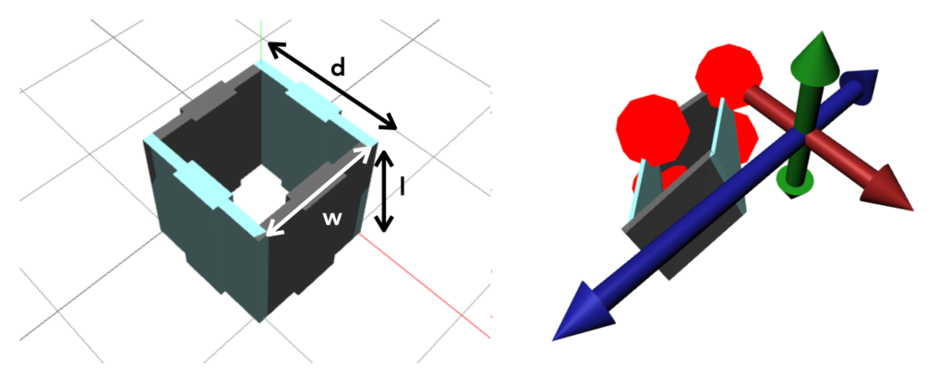
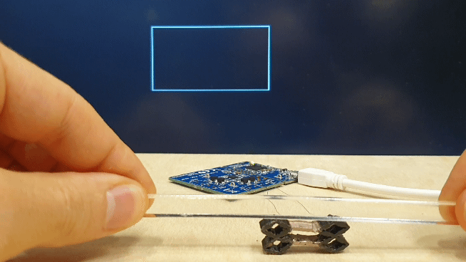
The sensing system consists of two conductive and two non-conductive opposing walls. Each conductive wall serves as an electrode. When a user interacts with the object and applies a force, the geometry and consequently the conductive shear cells deform. The distance and overlapping area between two opposing conductive walls change accordingly, resulting in a capacitance variance that can be measured via capacitive sensing:
The capacitance 𝐶 (in Farads) between two electrodes (i.e., two conductive walls) is given by:
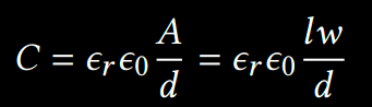
…where A is the area of overlap of two electrodes (in m²), 𝜖𝑟 is the dielectric constant, 𝜖0 is the electric constant and 𝑑 is the separation between the plates (in meters). In this scenario, 𝑙 and 𝑤 are the length and width of the conductive walls. Unlike using capacitive sensing for touch input, the capacitance variances are much smaller due to a small cell wall size and less conductive electrodes made with conductive filament. The resistivity R Ω of a cell wall can be calculated with:
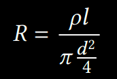
…where 𝜌 is the resistivity constant of the filament (Ω cm), 𝑙 is the length of the filament (cm), d is the diameter of the filament (cm²). Note that the contact resistance between a probe and the conductive filament results in a higher resistance reading than it is theoretically possible. There is additional variability depending on the print speed during fabrication.
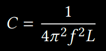
Due to the diminished conductivity of 3D printed electrodes, traditional methods like time-based capacitance measurement lack precision and are unsuitable for this application. Therefore, a resonance-based approach was employed, composed of an LC resonant circuit, including an inductor and a capacitor (i.e., two conductive walls). By precisely measuring the resonant frequency (𝑓 ) of the circuit, the capacitance (𝐶) between two conductive walls can be calculated using the following formula, where 𝐿 is the known inductance of the inductor:
Subsequently, the 1st formula can be used to interpolate the deformation of the conductive shear cell. The resonance-based approach has two major advantages. First, it is less susceptible to electromagnetic interferences (EMI), thus having a better signal-noise-ratio (SNR). Second, it allows the capacitance to be measured over a wide range (1pF to 250 nF) with an ultra-high resolution ( 10−15 fF).
1.2) Software Implementation
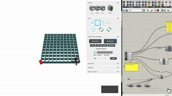
To allow users to create and fabricate objects and compliant mechanisms with integrated sensing capability, we implemented a 3D voxel-style editor, extending from the editor for metamaterial mechanisms. The goal is to help users interactively place and arrange conductive shear cells within an object’s internal geometry according to their sensing needs. The editor was created with Node.js and a three.js graphics framework for rendering the geometries. Rendering of 3D printable .STL files was done in modular hierarchical OpenSCAD script files. The editor exports the cell geometries as OpenSCAD script commands to render a cell with the specific parameters.
1.2.1) Auto-placing Conductive Shear Cells
To facilitate the design process, this custom editor can automatically place conductive shear cells based on a user’s intended interactions with the object being designed. We adapt the simulation function in the metamaterial mechanisms editor, which computes the deformation of an object’s geometry when a force is applied. This relies on a finite element solver, Karamba, a plug-in for Grasshopper (included in Rhino 6). We use deformed geometry vertex data from Karamba to calculate the distance and overlapping area change for each pair of opposing walls within the geometry.
We then use the 1st formula to obtain the “theoretical” capacitance variance for opposing walls. The heuristic used for evaluating the effectiveness of a cell sensor is the extent to which its capacitance changes – the larger the variance, the more optimal that position is to contain a sensor. Depending on the number of conductive cells desired by the user, the editor can automatically convert cells in the required number of positions into conductive shear cells.
Since vertices in a wall might not remain coplanar after deformation, and opposing walls may no longer be parallel, it is not straightforward to identify two representative planes to be used for distance and overlapping area change calculation. In the current implementation, we exploited two approximation methods to estimate the values.
1.2.2) Distance Change Estimation
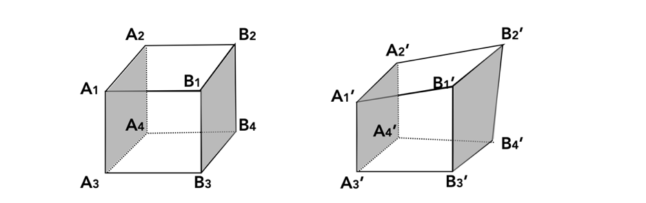
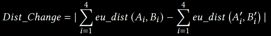
For the distance change estimation, instead of using the distance between two planes (or walls), we compute the sum of distances between four vertex pairs at the corners of two opposing walls. For example, as shown in the above figure, the distance between left and right walls (highlighted in grey) is defined by:
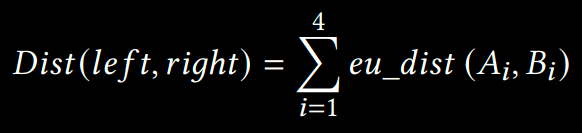
Therefore, the distance change after deformation is given by:
We used the Euclidean metric to calculate the distance between two vertices in 3D space.
1.2.3) Overlapping Area Change Estimation
Similar to our distance change estimation, we use four vertex pairs at the corners of two opposing walls to estimate the overlapping area change. As mentioned, four vertices within a wall may not be coplanar after deformation. Thus, we first derive best-fit planes using the four vertices in a wall by minimizing the sum of the quadratic distances (perpendicular to the plane) between the planes and the vertices. This can be solve by calculating the singular value decomposition of the vertices’ 3D coordinates. We then project the original vertices (e.g., A1) onto the fitted planes (Figure below - left) and obtain the projected vertices’ coordinates (e.g., A1p).
Since opposing planes may no longer be parallel after deformation, we then project the vertices on one fitted plane (e.g., A1p) to the opposite one (e.g., A1p’). For each cell, the outcome of this projection is two coplanar quadrilaterals. All the points on the plane are then rotated to lay on the x-z plane, such that we can reduce the problem to 2-dimensions and use the Sutherland-Hodgman polygon clipping algorithm to identify the overlapped polygon (Figure above - right). The overlapped area can be calculated using the shoelace algorithm. Given the 1st formula, we can estimate which pair of shear cell walls will have the largest capacitance variation due to a deformation event by dividing the overlap area change estimation over the distance change estimation for each cell. Within a cell, there would be two pairs of opposing walls (i.e., left and right, front and back). We used the one with a larger capacitance change to represent the optimality of that cell position as a sensor.
2) Capacitive sensing in 3d printing
2.1) Hardware Implementation
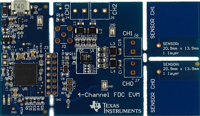
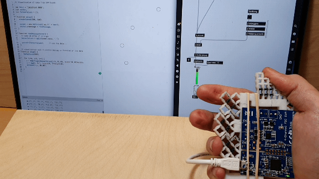
A resonant-based capacitive sensing chip (FDC2214, Texas Instruments) was used with the FDC2214EVM Evaluation board.
It can achieve precise capacitance measurements on four input channels with a sampling rate of up to 13300 samples per second. The chosen sampling rate was 100 Hz, with an applied exponential smoothing (a special case of IIR low-pass filter), after the data was received via serial. A 4:1 multiplexers (FSUSB74, ON Semiconductor) was also validated to measure more conductive shear cells simultaneously.
The code to use this board is available here:
github.com/mitmedialab/TI_EVM_logger
…and a generic data visualisation interface is available here:
editor.p5js.org/CedHon/sketches/4pFRCAyIQ
2.2) Characterization
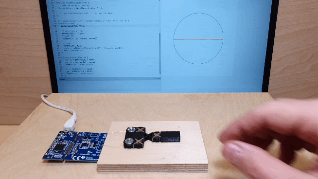
To test the capacitive sensing performances, the same basic capacitive cell structure was fabricated at varying sizes and wall widths:
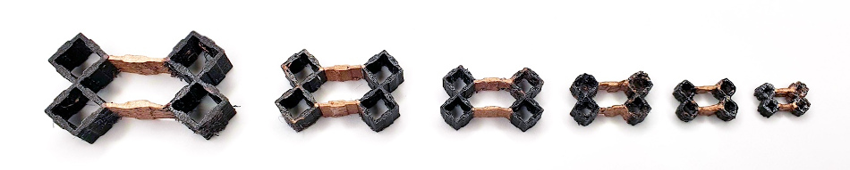
As anticipated, larger cell walls perform better as sensors. The smallest conductive structure that had a usable capacitance changes and mechanical viability was 5mm by 5mm by 0.5mm.
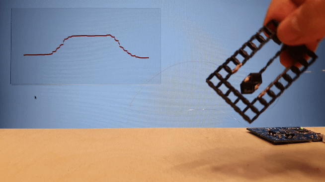
A simple test system was built to deform the 3D printed mechanism without having to physically interact with it, as this would influence the capacitance result. Each basic capacitive cell structure was then connected to the sensing hardware and the capacitance was measured at intervals of wall separation distances:
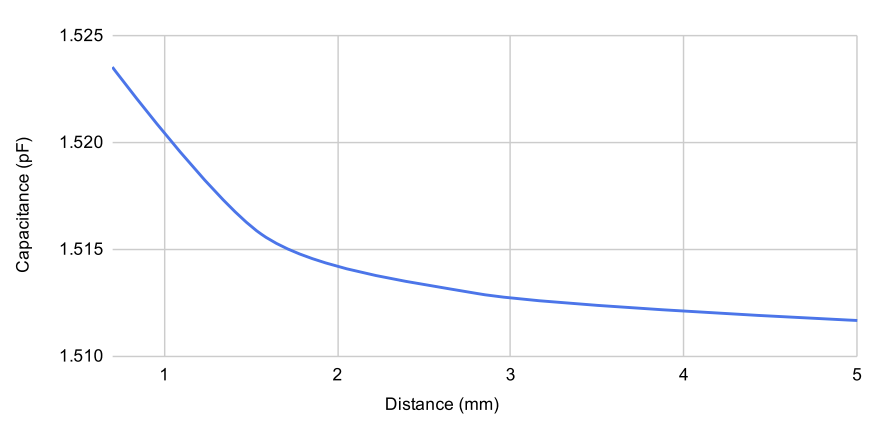
The outcome of the smallest conductive wall structure that had detectable capacitance changes at the chosen sensing resolution is visualized below. As expected, capacitance values have an inverse relationship with the distance between two opposing cell walls.
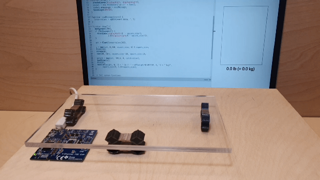
3) Visualizations & applications
Multiple interactive interfaces were fabricated to demonstrate or illustrate the concept and the possibilities. Each application demonstrates the use case of one or more of interactions enabled by the sensing approach.
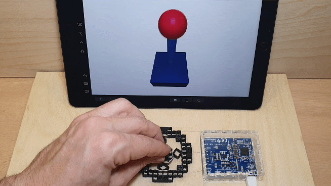
3.1) Joystick
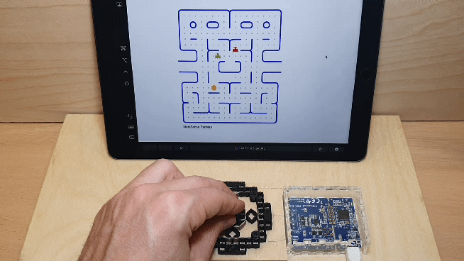
Created as a monolithic tangible interface, it can sense magnitude and direction. In this use case, four conductive cells were used and a regression model converts the combination of capacitance values at each point into control signals to play a game of Pac-Man via serial. The basic structure of conductive shear cells this mechanism can serve as a module for designers to build on and design a wide array tangible controls (e.g., creating a taller grip for the joystick, or making various handle shapes) and prototype various affordances. For instance, a designer could use this technique to create unique controllers for people with limited grip strength in particular directions.
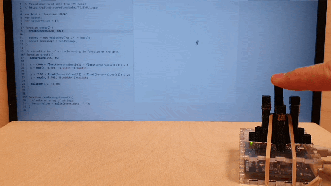
3.2) Accelerometer
Another benefit of this technique is its ability to combine fabricate sensors into the structure of single part compliant mechanisms. We demonstrate an accelerometer. When acceleration is applied the center “hammer” will swing towards (or away) from the conductive cell on the bordering wall. The change in capacitance can then be used to calculate the acceleration. While this is one example of a sensor, it is possible to fabricate single part sensors of many
types (humidity, temperature, etc.) in a similar manner.
3.3) Music Controller
In the field of HCI, deformable interfaces have gained traction and resulted in a number of works. In this application, we demonstrate that this technique allows deformable tangible interfaces to be quickly prototyped. This affords designers with the ability to test and tweak the ergonomics and performance of their design with precision and minimal manual labor. In this use case, we developed a control input for a digital synthesizer. The thumb portion is designed to shear and compress to mirror the thumbs movements, while the other fingers simply compress. We also added a passive metamaterial padding on the palm side of the controller to support a firm grip. The deformation at each finger is then communicated to a Max 7 patch to influence the parameters for musical synthesis. Shown below are the multiple rounds of trials performed to achieve a comfortable grip. The iterations were printed without conductive cells until the grip was correct, thus saving material cost.
3.4.1) Bending
3.4.2) Scale
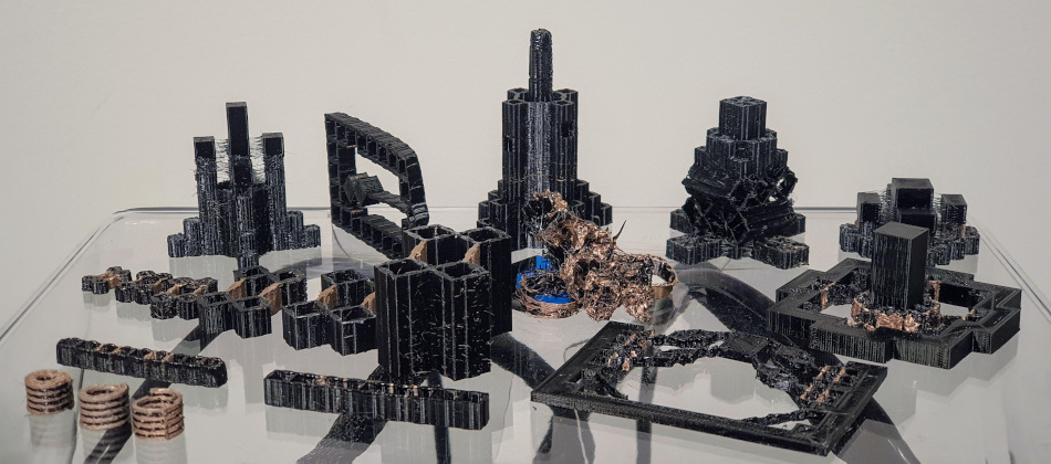
[ Failures ]
Of course, this project came with a lot of failed attempts, here is a “cemetery” with some of them:
4) Opening
A next obvious step is to incorporate actuation in these interfaces.
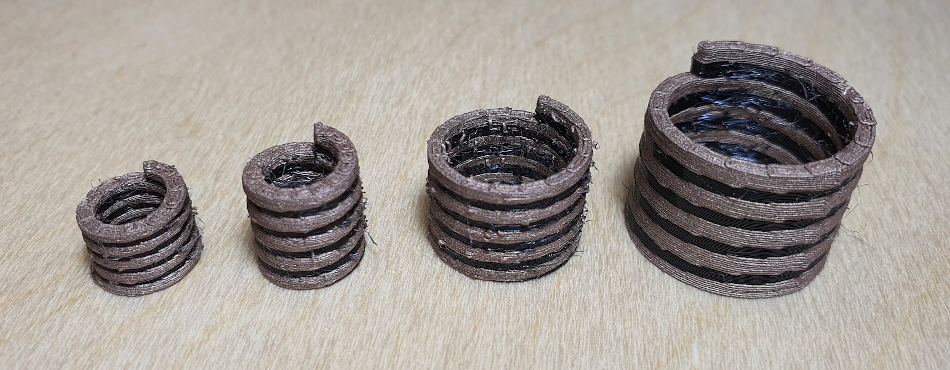
Haptuators being important to test, the 1st exploration has been to print coils to make solenoids:
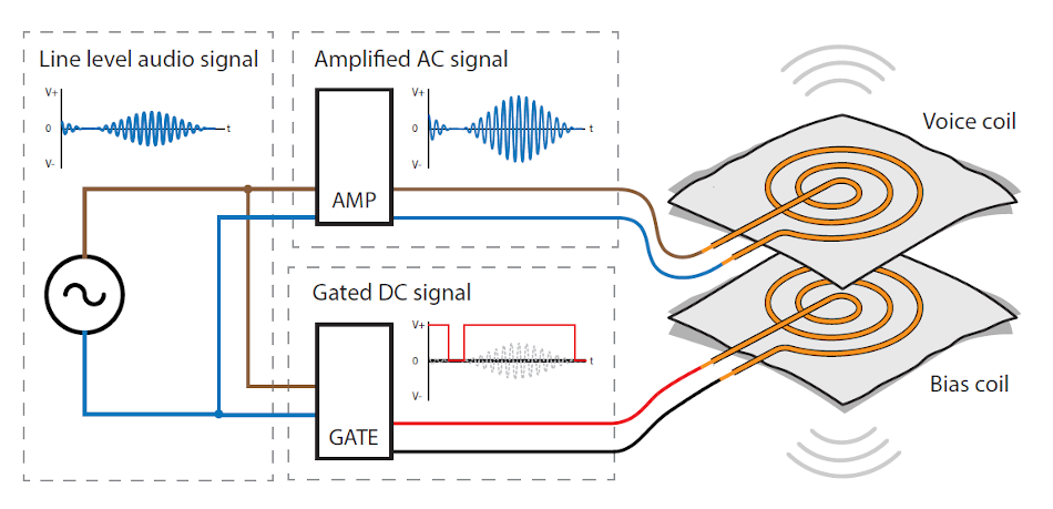
The ideal actuator would not even need a magnet as in SonoFlex (+ patent from the 90’s):
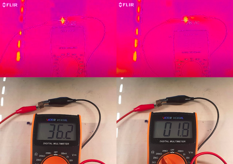
A great amount of current is necessary, and the resistance is still too high.
Here are some measures:
- 5mA @ 36V : no particular heat (26-27°C)
- Conductive part = 1.72 x 1.29 mm cross section
A pivot might be necessary, and another approach is being explored:
→ What if we could 3d print with electrical wires?
Some of them use shields made of materials that exist as 3d printing filament.
A first test is available in the latest logs, but it still needs some experimentation…
To be continued!