Week 08 - system demonstration
group page // repo source files // objectives
Contents
- meta
- updates
- geometry - tiles and connectors, in-house vs out-source
- error and hierarchy
- ring oscillator - Shravika’s design, 4x4 concept design and 3d implementation
- more dice work
- tooling - idc compliant pin connector forming tool
- claw gripper - documentation
meta >
- recap from last post
- new tiles (up to 7 tiles, 3 macro-tiles)
- automatic placement between 50% to 90%
- need to start data collection to check reliability
- geometry
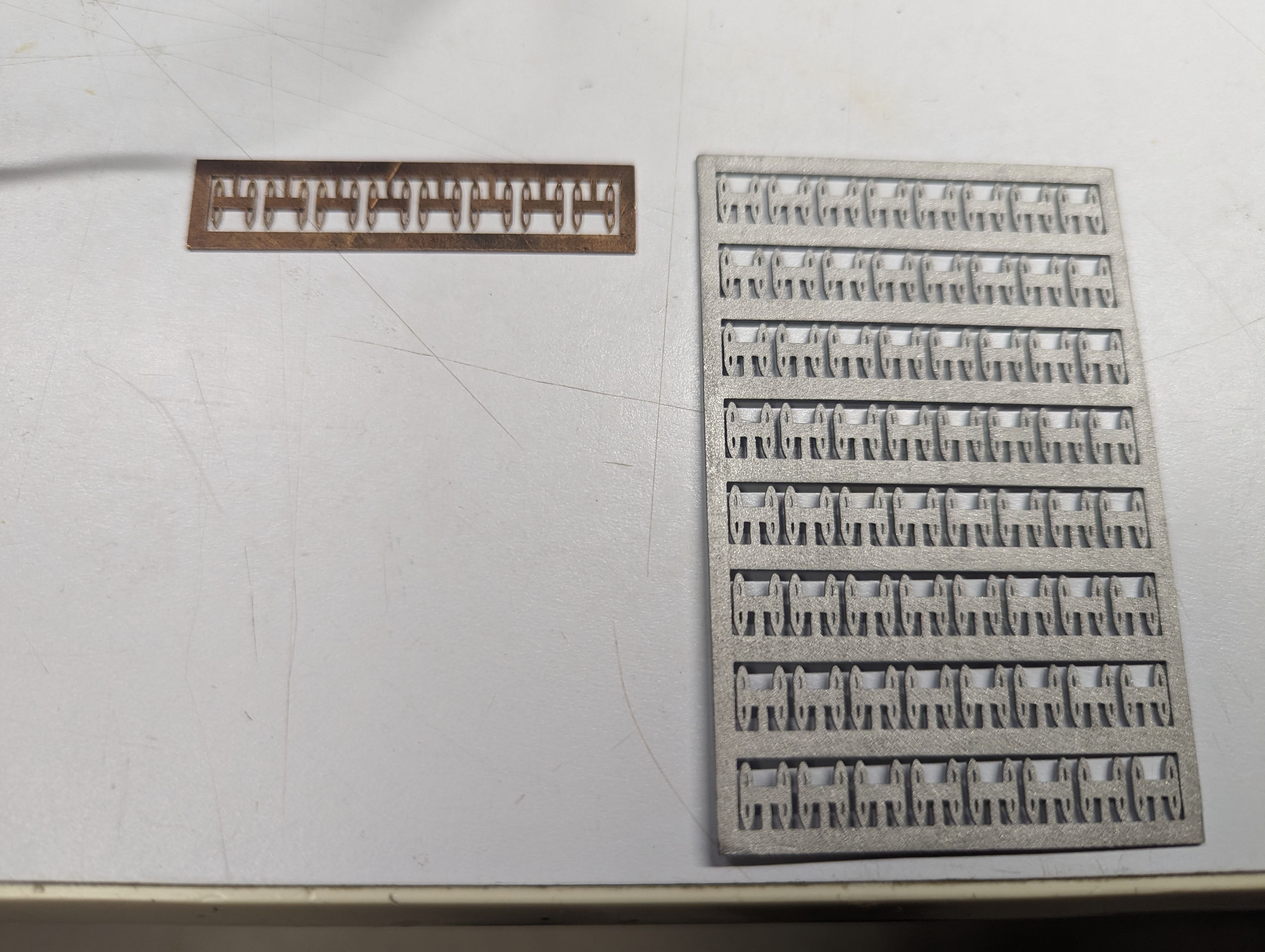
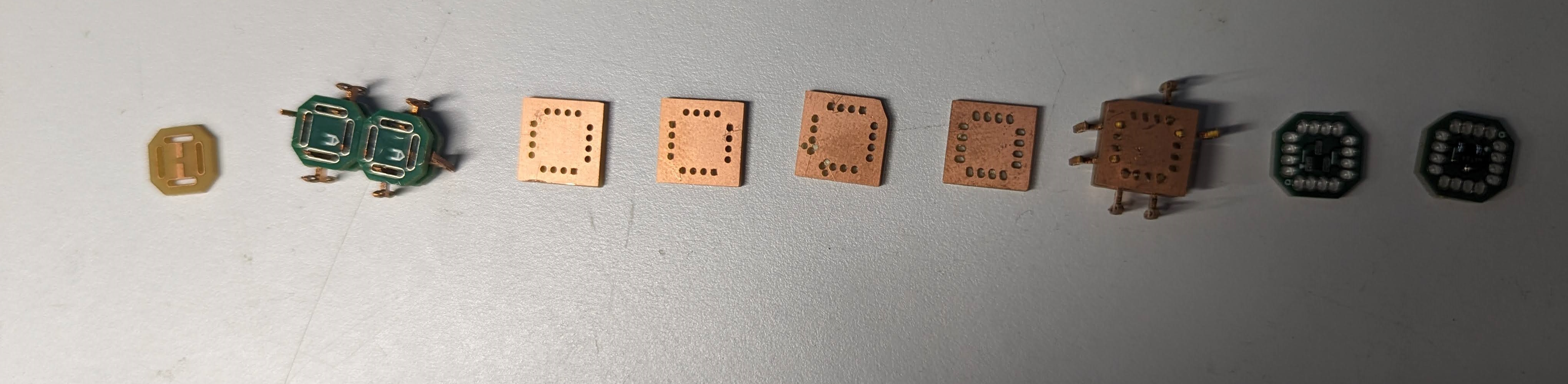
- ordered h connectors from pcbway (as-milled and tin-plated)
- pcbway can’t do under 0.5mm features apparently
- they can 3d print metal at the requested features, some resolution issues
- connector and tooling
- IDC 0.1 form tooling for compliant contact
- ring oscillator
- Shravika implemented a ring oscillator
- I’ve been working on shrinking circuits to fit 4x4 form factor, noting some routing limitations with the current tiles
- claw documentation
- discrete electronics hierarchy, error correction
- 3-layer powered structure
- definition of structure hierarchy (tiles vs macro-tiles vs blocks)
- errors at tile placement, error at block level
updates >
machine placement >
3-layer structure using fabricated IDC >
ct scan of fabricated IDC >
new tiles >
ordered some new macro tiles (4x4, 4x8, 8x8) and new resistor tile (1206_vert). new macro tiles feature no border, which enable them to tile just like the 1x1 tiles. new resistor tile features integrated power on one of the terminals, and can be rotate 180 deg to connect to vcc or gnd.
new tiles - batch 2 >


old tiles - batch 1 >


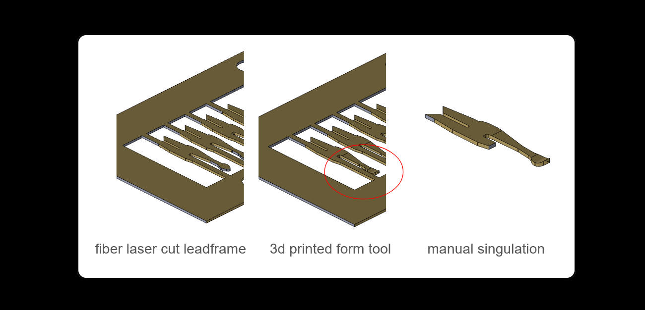
geometry - tiles and connectors, in-house vs out-source >
under economical and tolerance constraints, pcbway and other pcb houses are perfectly suited for outsourcing tiles to.
pcbway and like seem to be good for connectors as well, especially for queuing post processes like electropolishing and electroplating; in-house procedures would require a whole additonal setup, replicating beaker chemistries that are common in industry.
however, recent experiments with outsourcing connectors to pcbway have shown that there is a 0.5mm feature limit (both clearance and width), which makes it impossible to fabricate the connectors as is. this is in addition to the cost, which is relatively high compared to sourcing sheet metal for the fablight (though perhaps, post-processing included would make the costs somewhat comparable).
as the in-house connectors are “good enough” as-is, it seems that fabricating in-house is still the way to go. production as we shrink to smaller size-scales will become an even more interesting challenge; we’ll likely need to leverage mit.nano more heavily to achieve scale production.
a neat aside, pcbway can’t laser cut down to that resolution but can 3d print the same file; the resolution does suffer and may be tunable for the process, but the aluminum is quite brittle so not certain if it would actually produce good connectors.
error and hierarchy >
tile error correction >
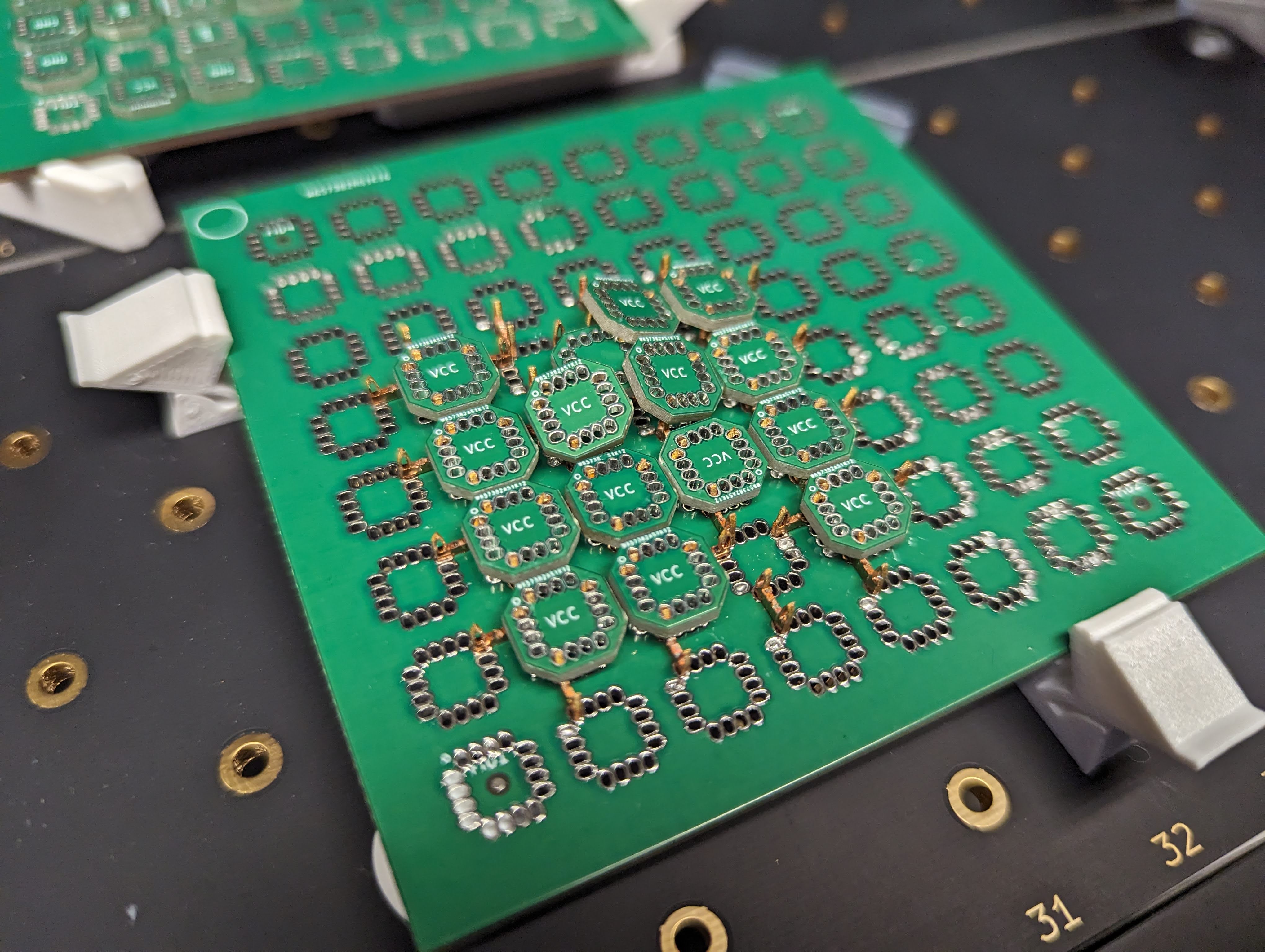
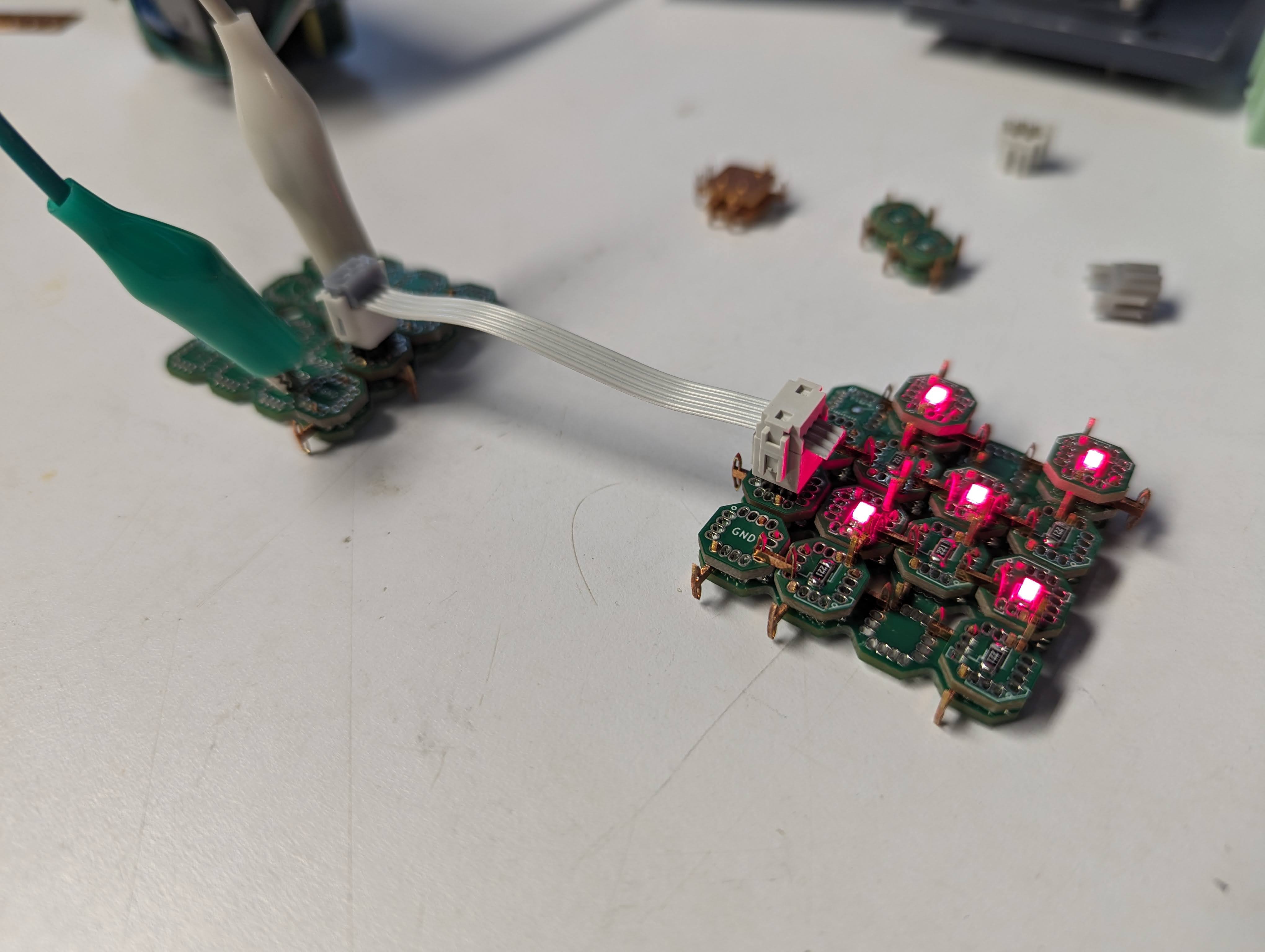
during assembly testing, I’ve gotten great results, in the best case 14/16 or 15/16 successful placements using a soldered connector substrate.
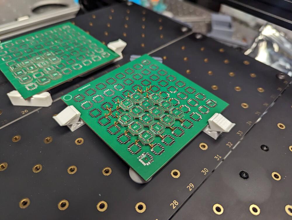
However, I’ve also observed interesting errors, all recoverable to some degree. one very interesting error started with an incomplete place, which somehow jumped the tile out and shorted 4 adjacent cells. importantly, subsequent placements were successful and the machine recovered w/o damage to the connectors, yet this particular error would coincidentally short the power and ground pins, as the tile fits in between cells and successfully connects that way.
block error correction >
going from 10 to 10,000 tiles, statistically it seems very likely that there will be non-zero tile placement errors. I’m planning to build in error correction systems and unit tests along the way, but it’s likely we’ll need coarser levels of error correction (block level error correction) and easy replacement at the block level.
this is one of the major functions for the macro-tiles, and why I’ve designed them to adhere strictly to the 10mm cell grid size, so they can be placed next to each other.
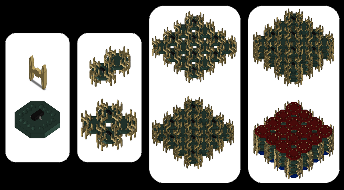
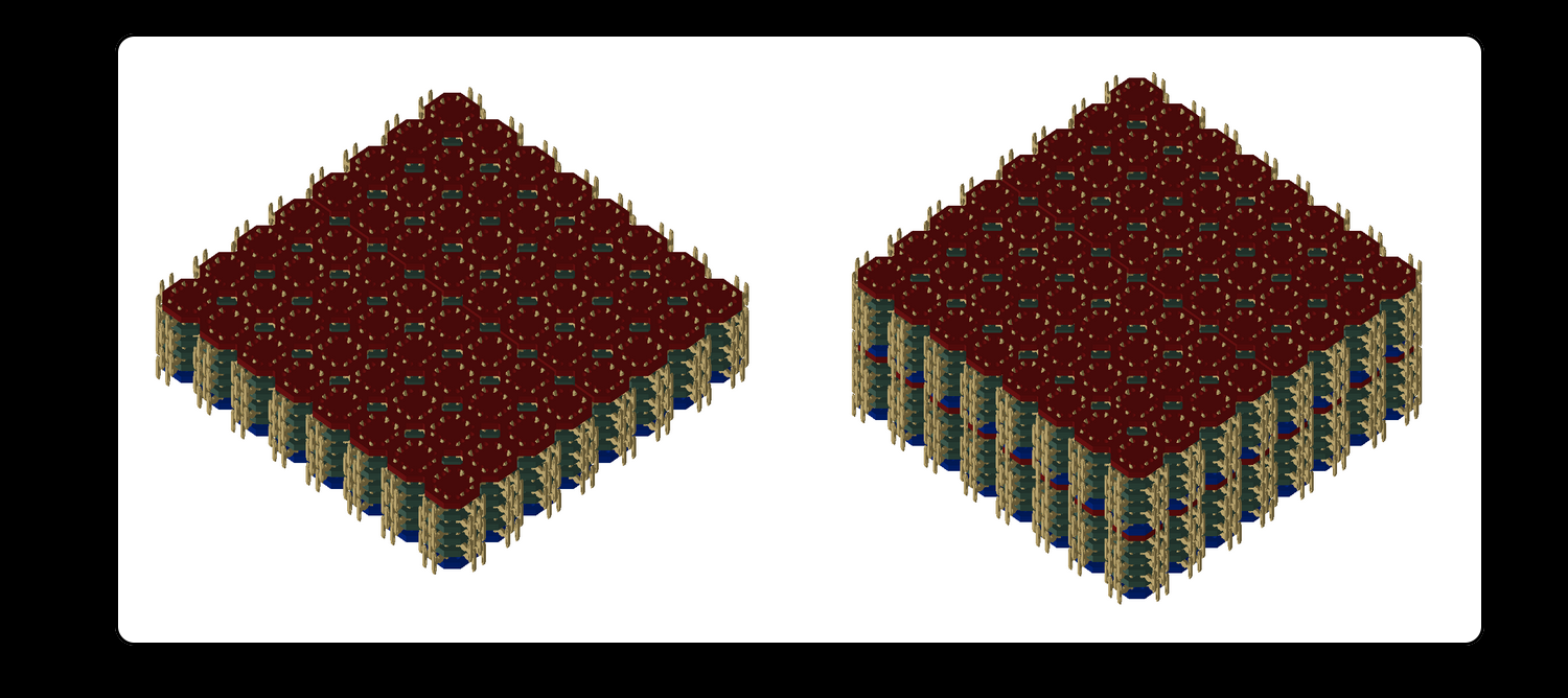
top, tiles building up to 4x4xh sandwich between macro-tiles, in red and blue; bottom, block-sandwiches neatly packed next to each other and height-wise too
ring oscillator - Shravika’s design, 4x4 concept design and 3d implementation >
Shravika Pendyala (my UROP) implemented a ring oscillator application circuit and has it working; found the resonance frequency to be ~2MHz. These FETs are being used for the SERV cpu. Packaging parasitics could be improved from these baseline measurements.
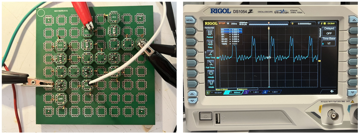
3-layer 4x4 concept design for compressing the ring oscillator from 8x8 to 4x4.
 PXL_20240413_200055577.cmp
 PXL_20240416_214004117.cmp
 PXL_20240417_230625194.cmp
 PXL_20240418_164104310.cmp
 PXL_20240418_164107808.cmp
 PXL_20240418_164113741.cmp
 PXL_20240418_164309129.cmp


A demonstration structure for 3d placement (a 3-layer powered structure):
more dice work >
 PXL_20240419_003155001.cmp
 PXL_20240419_010911095.cmp
 PXL_20240419_013722071.cmp
 PXL_20240419_013801131.cmp
 PXL_20240419_222215403.cmp
 PXL_20240420_174531866.cmp
 PXL_20240420_182648420.cmp
 PXL_20240420_182703863.cmp
 PXL_20240420_182707960.cmp
 PXL_20240420_221344805.cmp
 PXL_20240420_223621896.cmp
 PXL_20240421_050245015.cmp
 PXL_20240421_050255363.cmp
 PXL_20240421_051537026.cmp
 PXL_20240421_055129267.cmp
 PXL_20240421_055132253.cmp
 PXL_20240421_055151754.cmp
 PXL_20240421_062313469.cmp
 PXL_20240421_062317397.cmp
 PXL_20240421_062321682.cmp
 PXL_20240421_212839212.cmp
 PXL_20240421_212844126.cmp
 PXL_20240422_005353369.cmp
 PXL_20240422_005357982.cmp
 PXL_20240422_005622773.cmp
 PXL_20240422_005639722.cmp
 PXL_20240422_021811170.cmp
 PXL_20240422_021820021.cmp
 PXL_20240422_044421057.cmp
 PXL_20240422_173240484.cmp
 PXL_20240422_173241933.cmp
 PXL_20240422_173641651.cmp
 PXL_20240422_173643352.cmp
 PXL_20240422_173645705.cmp
 PXL_20240422_214642594.cmp
 PXL_20240423_135148721.cmp
 PXL_20240423_135153932.cmp
 PXL_20240423_142406554.cmp
 PXL_20240423_180132595.cmp
 PXL_20240423_184854453.cmp


tooling - idc compliant pin connector forming tool >
3-layer structure using fabricated IDC >
ct scan of fabricated IDC >
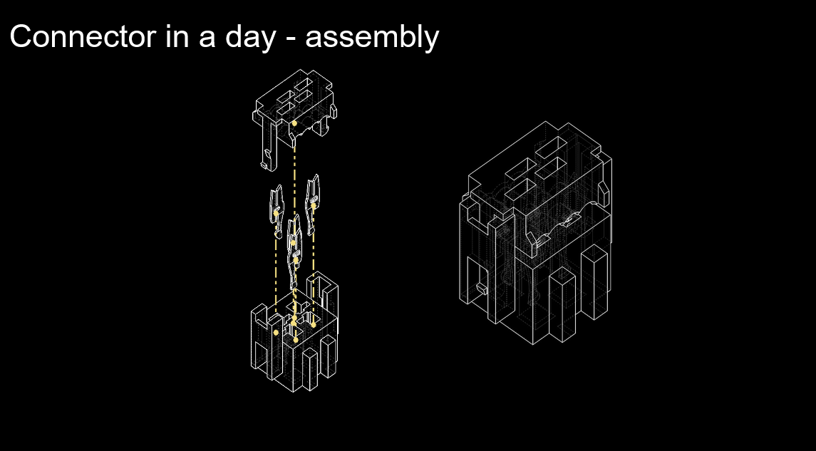
the IDC connector geometry requires forming contacts to create compliant pins that can wipe against a mated connector to form an electrical connection.
to achieve this, several stages must be aligned and mated. tool stackup, top to bottom:
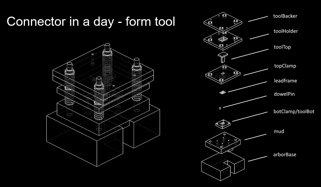
- toolBacker - constrains toolTop within toolHolder
- toolHolder - holds toolTop
- toolTop - designed with form geometry to fit compliant pin profile
- topClamp - clamps down on leadframe from top
- botClamp - other mating half of the clamp and includes pins for registration, also holds toolBot
- toolBot - mates against toolTop to form the leadframe
- mud - modular unit die, botClamp is installed using screws and can be swapped out; (term not used completely correctly here)
- https://www.dme.net/MUD/
- arborBase - base of the arbor press
taking stock of the components we have in inventory, designed the forming tool using 3/8” linear shafts and plain flanged bushings, which are plentiful and cost-effective should I decide to order more.
to constrain the bushing into each moving stage (toolBacker, toolHolder, topClamp), I iterated on a 1 deg drafted/tapered hole press-fit geometry which makes it easy to insert the bushing, but press-fits at the end of the geometry. under compression, the bushing is kept constrained in the stage. the geometry is modeled after crushribs, where the contact surface is reduced a bit using cuts for compliance. I found that 6 cuts were sufficient, and 4 still worked. adding additional cuts caused the press-fit to deteriorate.
the flanges caused some issues, leading to surfaces butting against each other prematurely, but I fixed that by adding some additional drafted/tapered hole standoffs.
after forming, the form tool appears to have transferred the geometry to the leadframe, creating a compliant pin geometry. however, a fix is wip because the action window wasn’t big enough, and due to the system not being flush, I ended up bending some of the idc contacts intended for displacing wire.
 PXL_20240412_160117901.cmp
 PXL_20240413_200032872.cmp
 PXL_20240413_200035023.cmp
 PXL_20240413_200036780.cmp
 PXL_20240413_200039496.cmp
 PXL_20240413_200045468.cmp
 PXL_20240413_200107258.cmp
 PXL_20240413_200113679.cmp
 PXL_20240414_221714050.cmp
 PXL_20240416_022202124.cmp
 PXL_20240416_022822707.cmp
 PXL_20240416_022903774.cmp
 PXL_20240416_033522926.cmp
 PXL_20240416_223839354.cmp
 PXL_20240418_163319002.cmp
 PXL_20240418_163357136.cmp
 PXL_20240418_163414362.cmp


here’s a ct scan of the resulting leadframe:
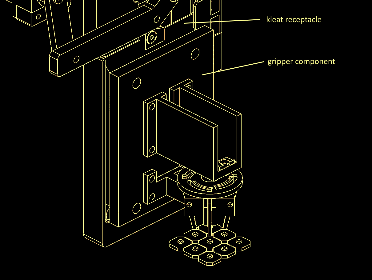
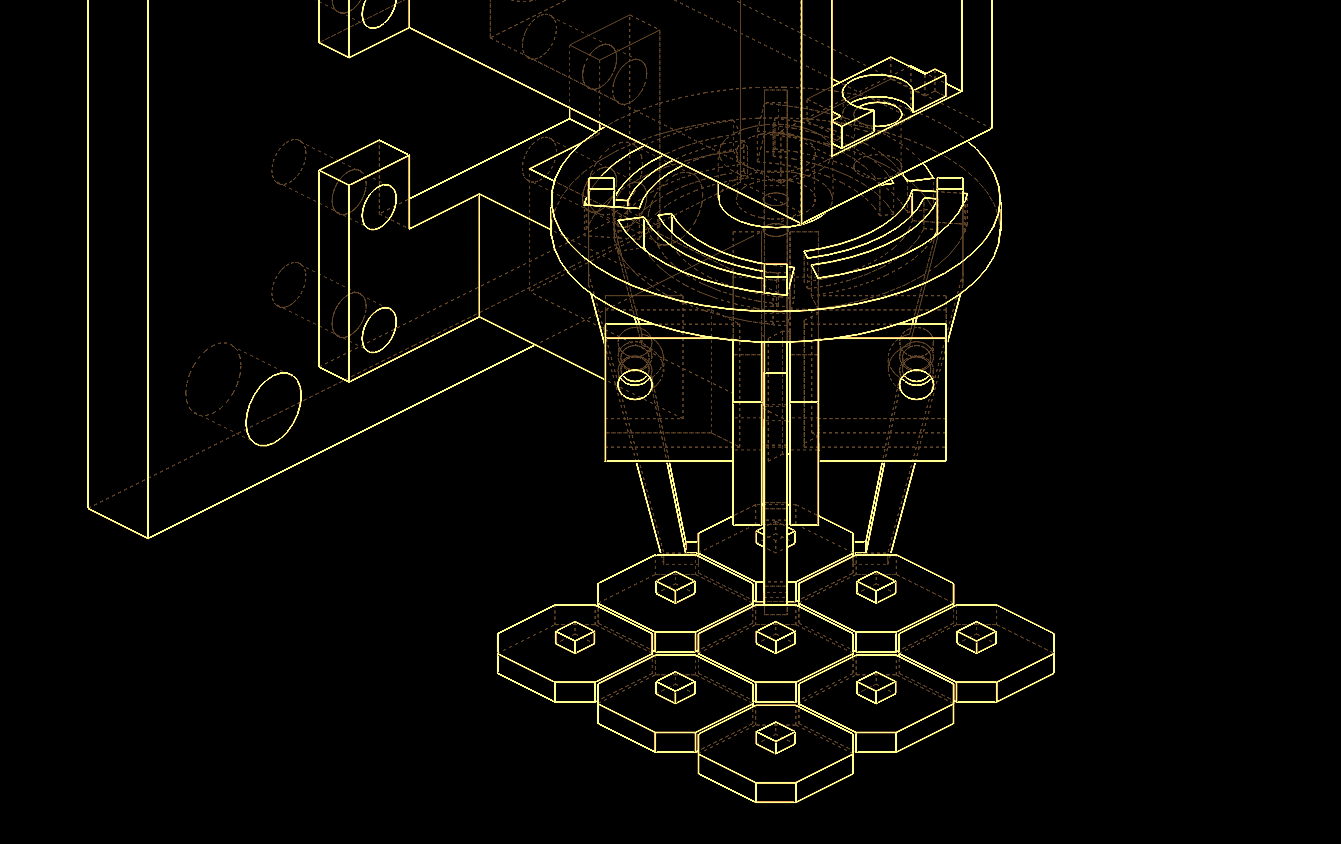
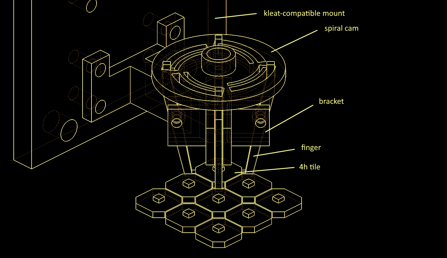
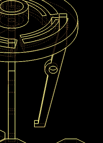
claw gripper - documentation >
the claw gripper is driven by a servo and intended for 4h_power geometry, which is 9.5 x 9.5mm.