Electronics Design
Testing our Electronics Design
Project Description
I worked on this in KiCAD. I picked KiCAD instead of the other two since I don't want to pay for fusion after my educational licsence.
I was also confused by svg-pcb. There isn't widespread tutorial on this online since it is a new platform. Therefore, as a beginner, I think KiCAD is the best option for me.
PCD board
KiCAD
This is the final iteration of the circut which is closely put together
Planning out the paths to see if I could connect all my pins. But the layout was not set. THerefore , the board looks very big since I am just playing around.
Switching to PCB side after schematic design. It looks like my schematic design shows that the pins are crossing over too much, so I rotated it.
Schematic Design
Final Schematic Design, where I added, a button, resistors, and a LED which would help with the general functions of the board.
I wanted to have two pin connectors, one with pins SCL SDA for I2C communication with a network of IMU / accelorometers. I am not sure how it would work, but this is what I decided that is correct
Simiply putting components in the schematic design page. Putting XIAO board, and putting a bunch of pin connecter modules to see which ones I want to use.
Testing Equipment
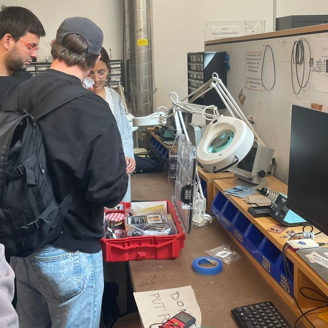 Simon showing his box of stuff !
 Testing the voltage on a 9V battery
 Testing the voltage on the 5V Xiao boards
 Trying to find the resistance of a random resistor