PCB Design
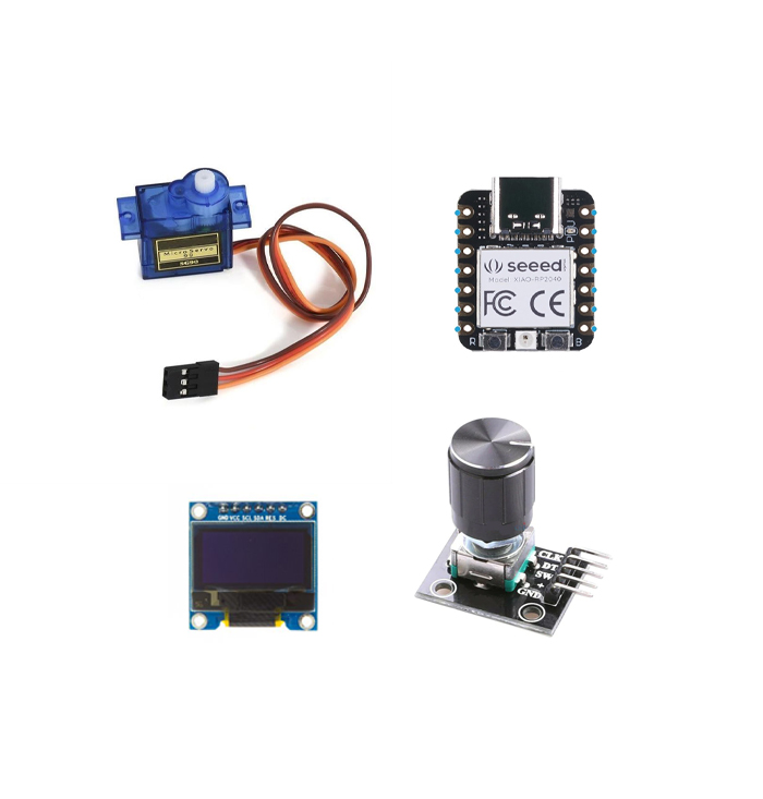
I’d like to use this week's assignment to start thinking about how to fabricate my printed circuit board (PCB) for my final project. Since I’m not quite sure what components I need for my final PCB, this prototype will be a balancing act of providing extra spots than I think I need for inputs and outputs as well as familiarizing myself with the KiCad software. I’ve never done any sort of electronics design and I’d never even touched a breadboard until a couple of weeks ago, so I’m aiming for something simple and feasible.There are a couple of components that I know I will need for my final: an oled display, at least one motor and a rotary encoder knob. I looked around the shop and found a couple of candidates to mess around on the breadboard with.
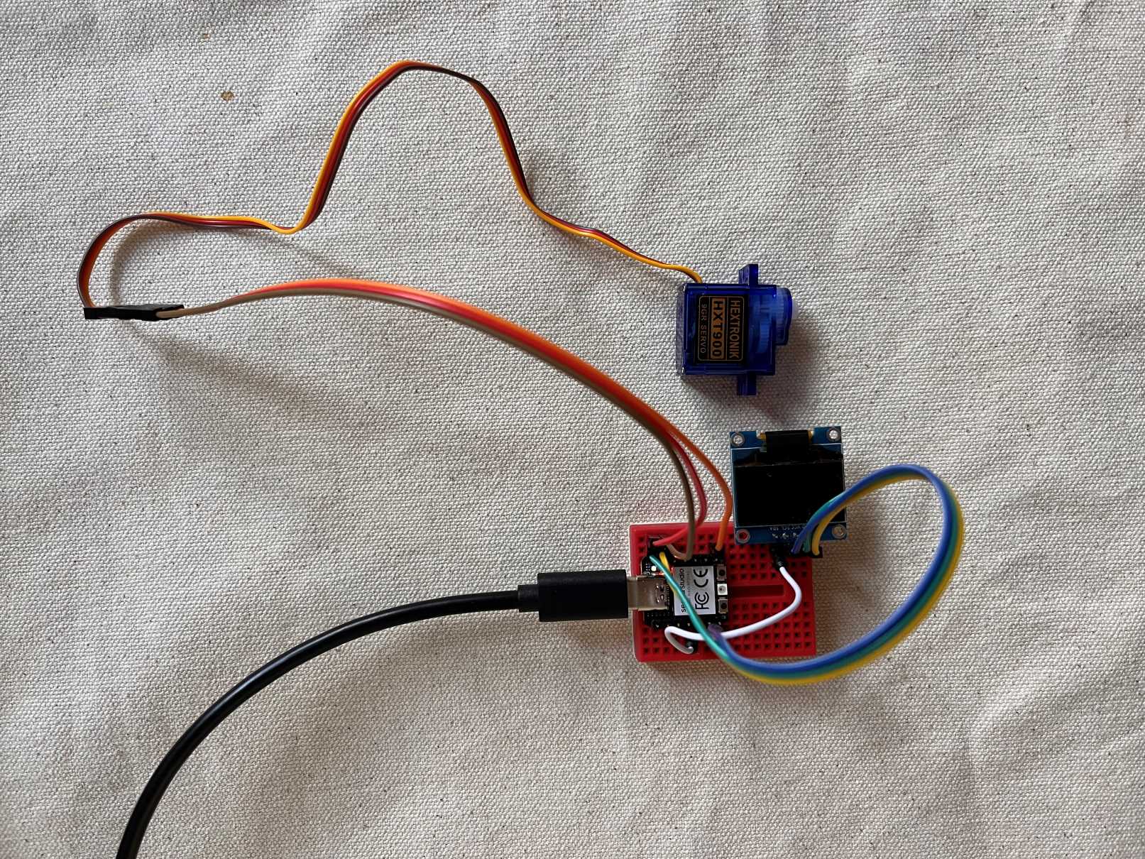
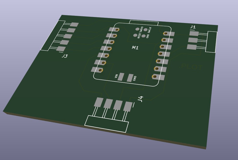
Now that I got the breadboard to work (at least enough) I used the wiring and logic as a sketch for designing my PCB. I used the components I found as constraints for designing my first PCB, because I’ve found that it's quite hard to design without a goal in mind (at least at my level of experience.)
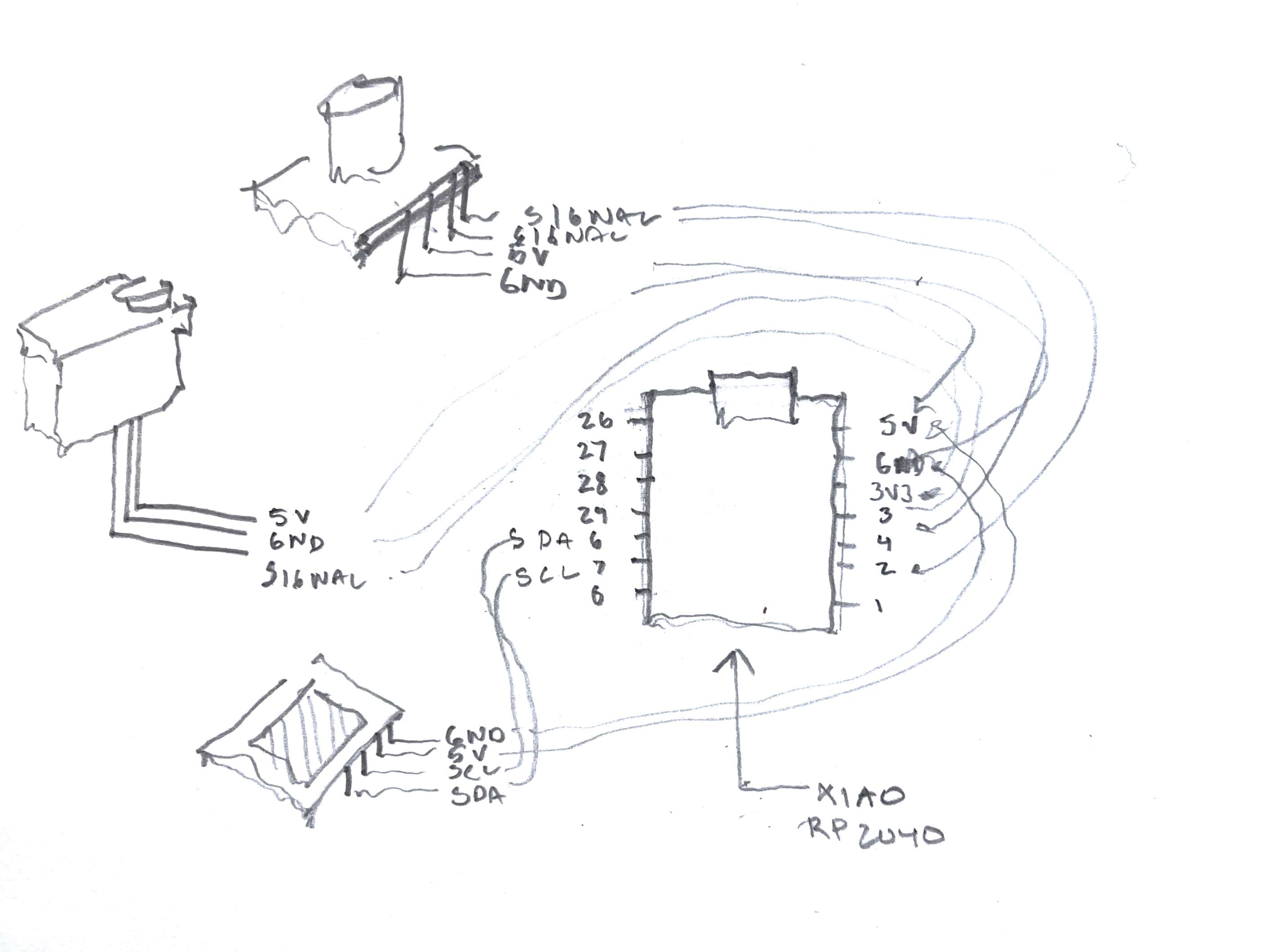
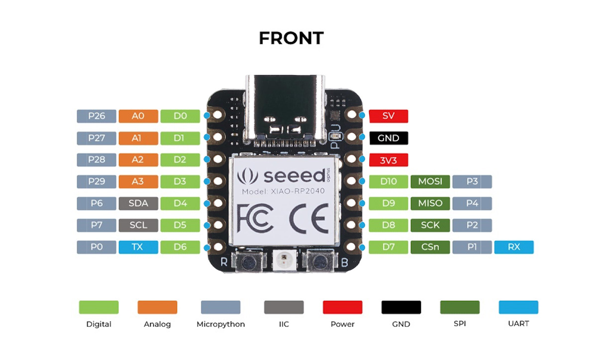
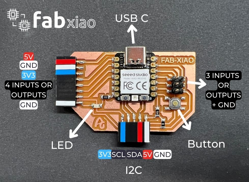
I referred back to the XIAO RP2040 Pinout diagram both to orient the breadboard and to begin thinking of a general layout for the PCB. The important placements will be the SCL and SDA and the grounding and power supply because the pins are kind of everywhere and easy to locate. Only the oled needs a SCL and SDA input so that’s what I used as my first constraint.
As a starting point I referred to the Fab Xiao which uses the same microcontroller and is layed out pretty nicely. The link can be found here: http://fabacademy.org/2020/labs/leon/students/adrian-torres/fabxiao.html
I generally like open-source platforms and don’t have experience in Fusion 360, so I opted to learn KiCad. Following both Anthony and Quinten’s advice on clean practices in schematic PCB design, I worked solely with labels instead of wire connections at this stage. Maybe it’s because I’m a beginner but this also required a lot of back and forth between the PCB editor and schematic editor as a tradeoff.
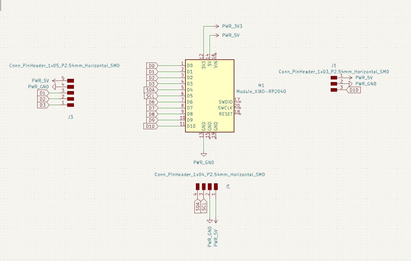
The XIAO RP 2040 from the Fab library includes the pads on the bottom of the device which made creating the paths a bit annoying in the editor stage. Going forward, I’ll find another way to locate the XIAO layout to make it a bit cleaner, but this is just the first iteration.
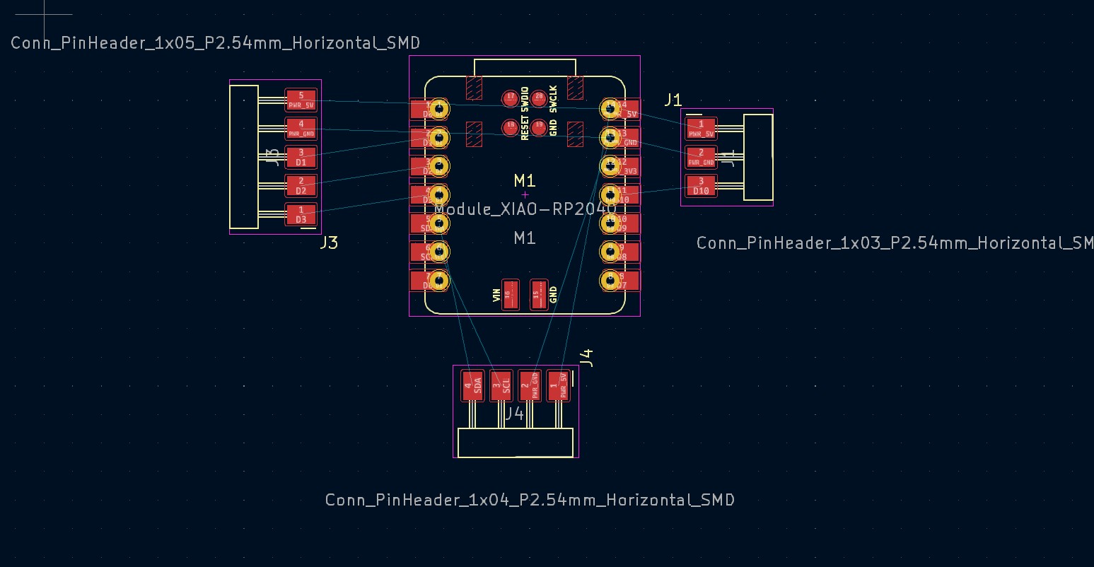
The 3D viewer was a bit underwhelming for this board in particular but I imagine it might be more helpful for more intricate boards and ones that might need cases.
PCB Fabrication
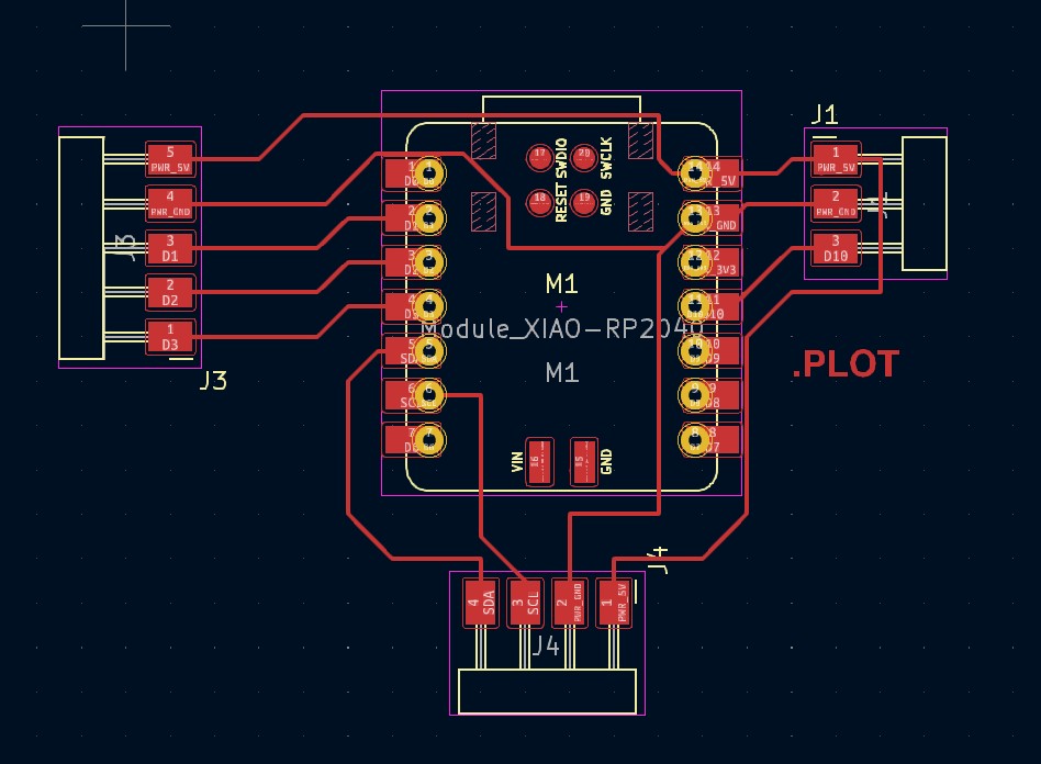
I exported my file as an svg and just kept the copper layer. I’ve used mods for Vinyl and small part milling so I generally know what the final png is supposed to look like.
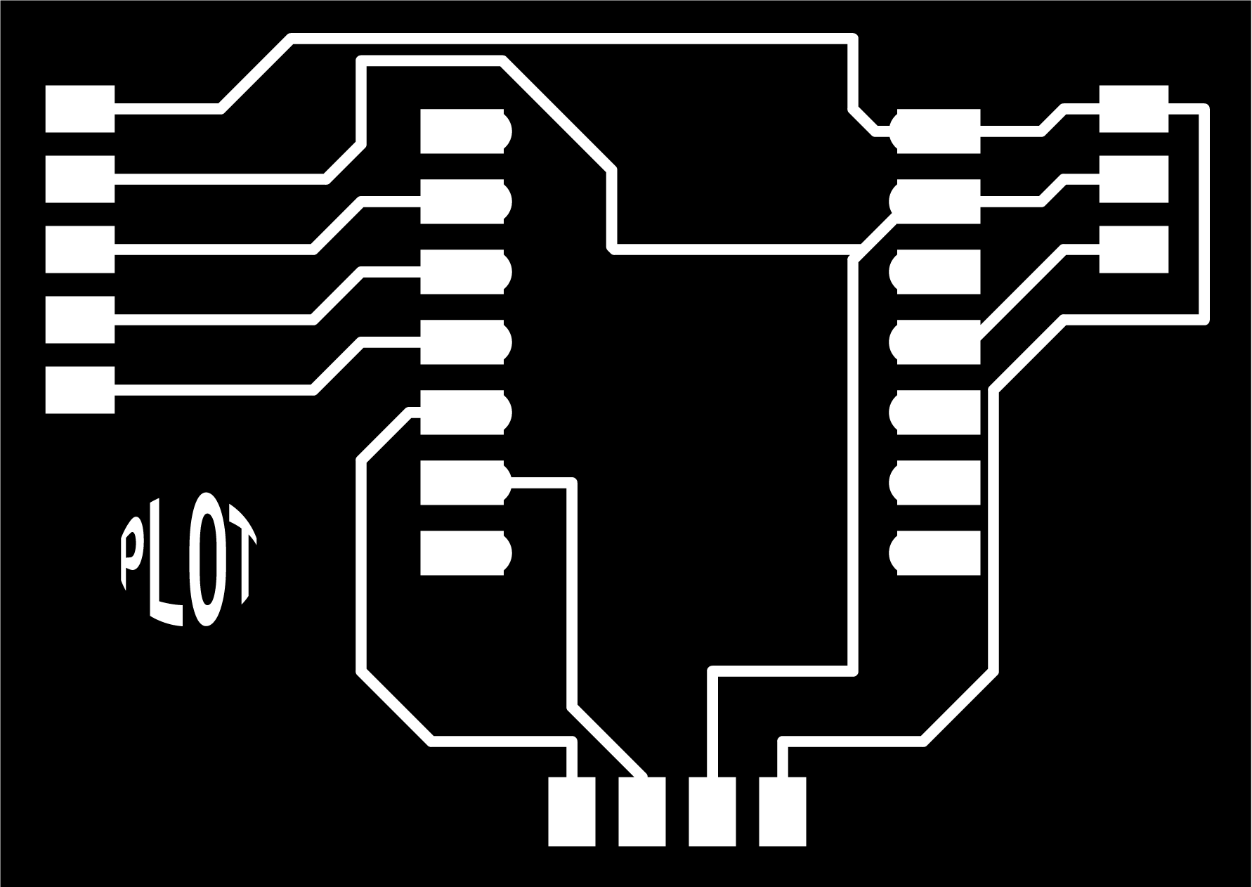
I’m not including the milling process because that’s for next week but I wanted to show the final product which is more or less a cleaner version of the breadboard prototype that I made. I chose to do this so I could use this week and next week as a two step process in refining my PCB for my final project. I think it’s helpful to have a working product to play around with before going into the next, more elaborate iteration.