Week 5
.jpg)
This week was challenging, frustrating, and full of work for me. In the end, none of my PCBs worked, but I really enjoyed the workflow and am confident that I will explore further and continue working on it in the coming weeks in addition to my assignments.
My first iteration was simply to enlarge the microcontroller by attaching two LEDs and connectors to each pin on the microcontroller. On the screen, it appeared to be very simple, and my goal was to simply learn some basic functions. I intended to do another pcb after this, which would be a little more logical in terms of functions.

I did my schematic and routing on KiCAD(I am sorry I lost the screenshot of the routing version for this one), after exporting it to SVG, I used Illustrator to prepare two seperate files for 'outline' and 'interior'
.png)
.png)
And miling and soldering journey started! Miling went all well, after several tests I was able to create a clean cut (I believe)
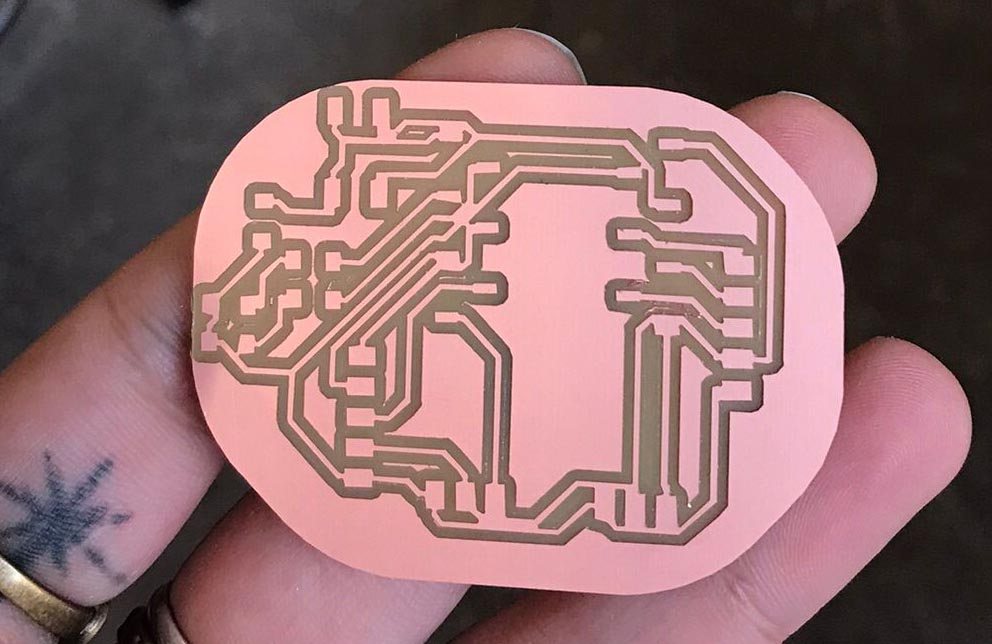
This was the result:
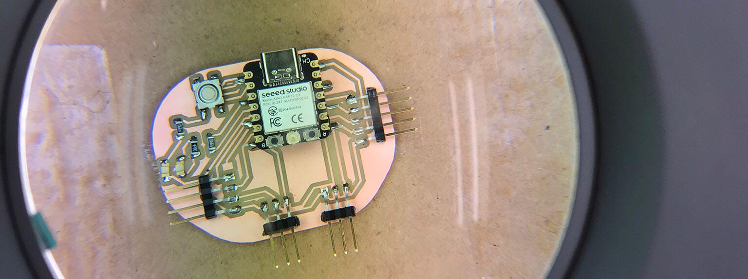
And then... It did not work... I was pretty sure I did everything correct LED orientations, button orientation, connectors, perhaps some lines were too close to each other... And for troubleshooting (I am happy I connected microcontroller through male connectors) I used cables to understand which pin creates the problem. And it was the GND pin. Well, all my components somehow connected to the ground... It wasn't helpful.
.jpg)
I desoldered all the LEDs and button and checked if everything is correct, it did not work. And I gave up on this one, wanted to try another one.
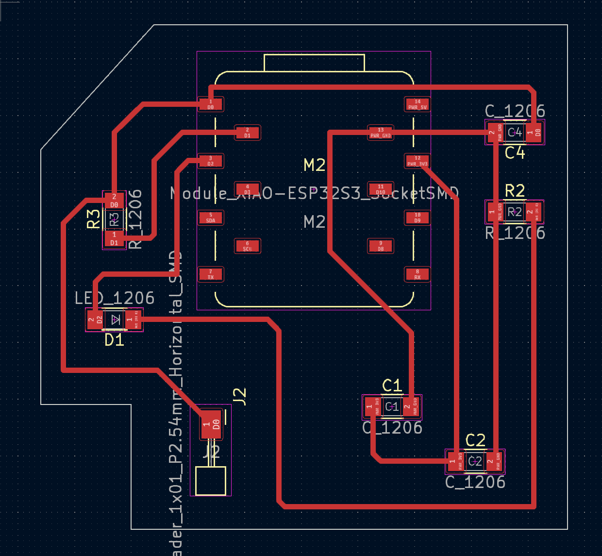
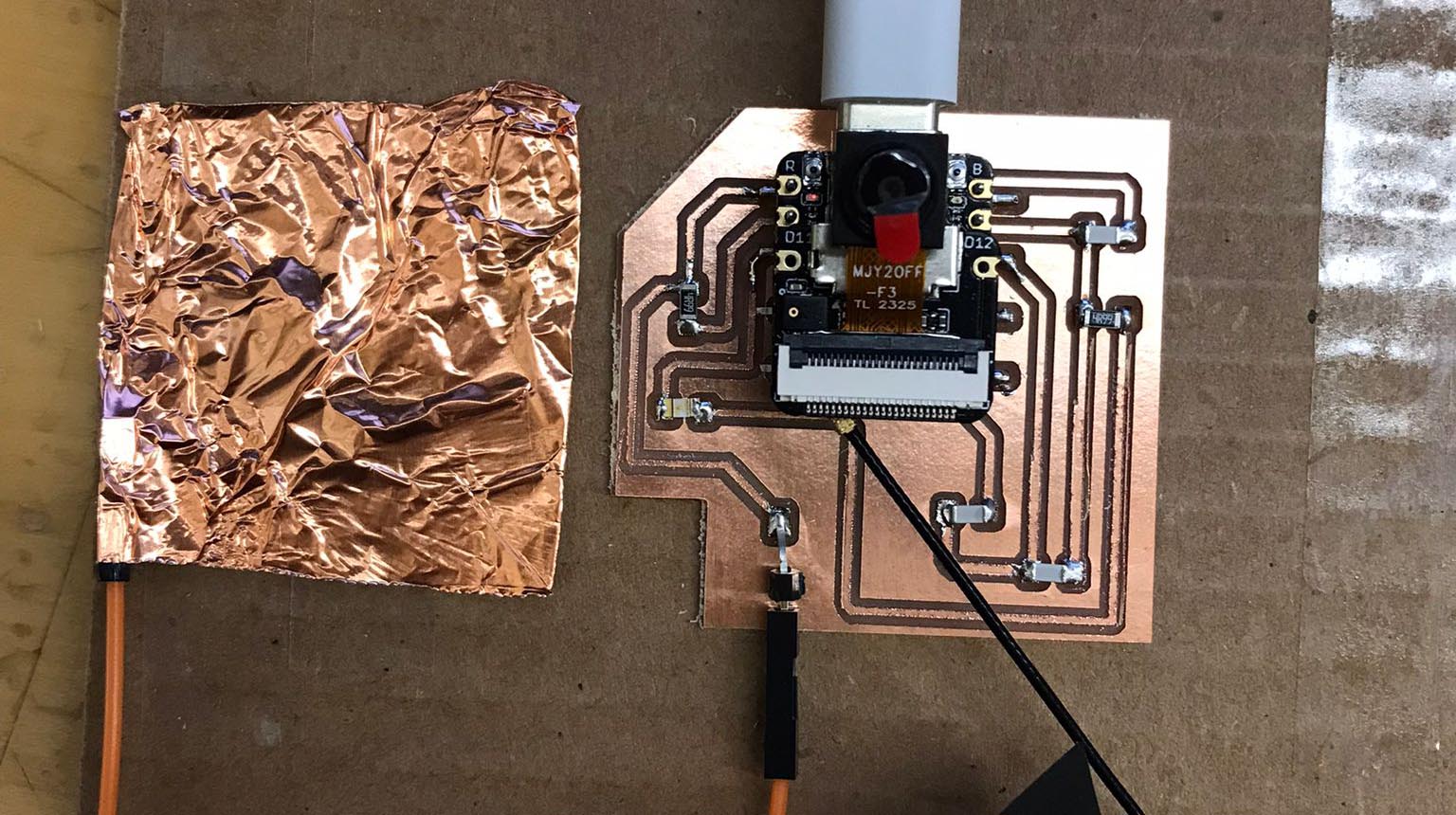
For my final project, I'm thinking about some on-skin devices that can detect pressure with sensors on the skin. I wanted to start with capacitive touch sensors, but I also had an ESP32 S3 with a camera module, and the idea this week for the pcb was that when you touched the copper, the camera would capture an image and send it to the computer. To accomplish this, I devised the following simple schematic:
.png)
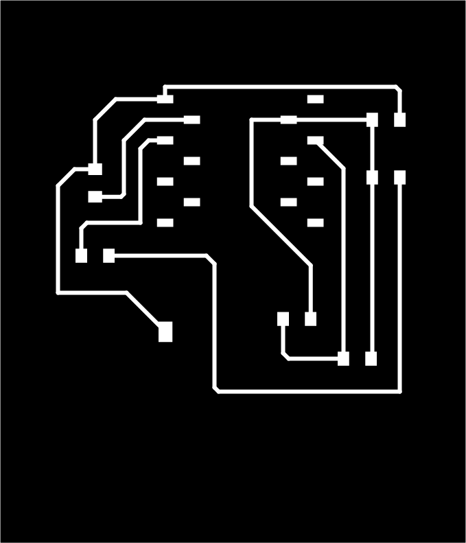

I miled it and I was super excited to try it out, but this one did not work as well. I tried to troubleshoot it with different methods like measuring voltage with multimeter or desoldering and soldering again but I could not solve the issue. I don't know what the problem is either. I will run more tests next week and hopefully make it work!
.jpg)
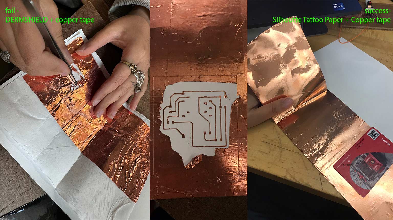
The part that I was so happy with it was the vinyl cut... I managed to cut the pcb layout on a transparent surface, haven't had time to solder and test it but for my final project I am imagining pressure devices on skin like temporary tattoos so it was the first step for me. Here is my journey with trial and errors. I used copper tape + Silhoutte Temprary Tattoo Paper!

As a group we tested miling all together as well!
.jpg)
The most time-consuming thing that happened to me was an error with my ESP32 microcontrollers (both C3 and S3) while I was trying to program the code portion of the assignment, it started giving the error below, it is still a mystery, I tried everything to fix it, everything I found on the internet but it is still not resolved... Jennifer was extremely helpful, and she got it to work on one of the shop computers, but the problem remains on my computer.