With the intrinsic goal of detection of PFAS, I aimed to target rapid, selective PFAS detection through the use of Lateral Flow Assays and Filters. My goal for extending my original focus to filters was to target the capture and detection of PFAS, which can present a possible solution for PFAS removal from water supplies in homes and industries.
Electronics
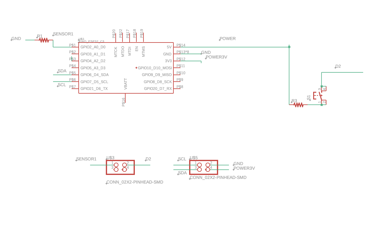
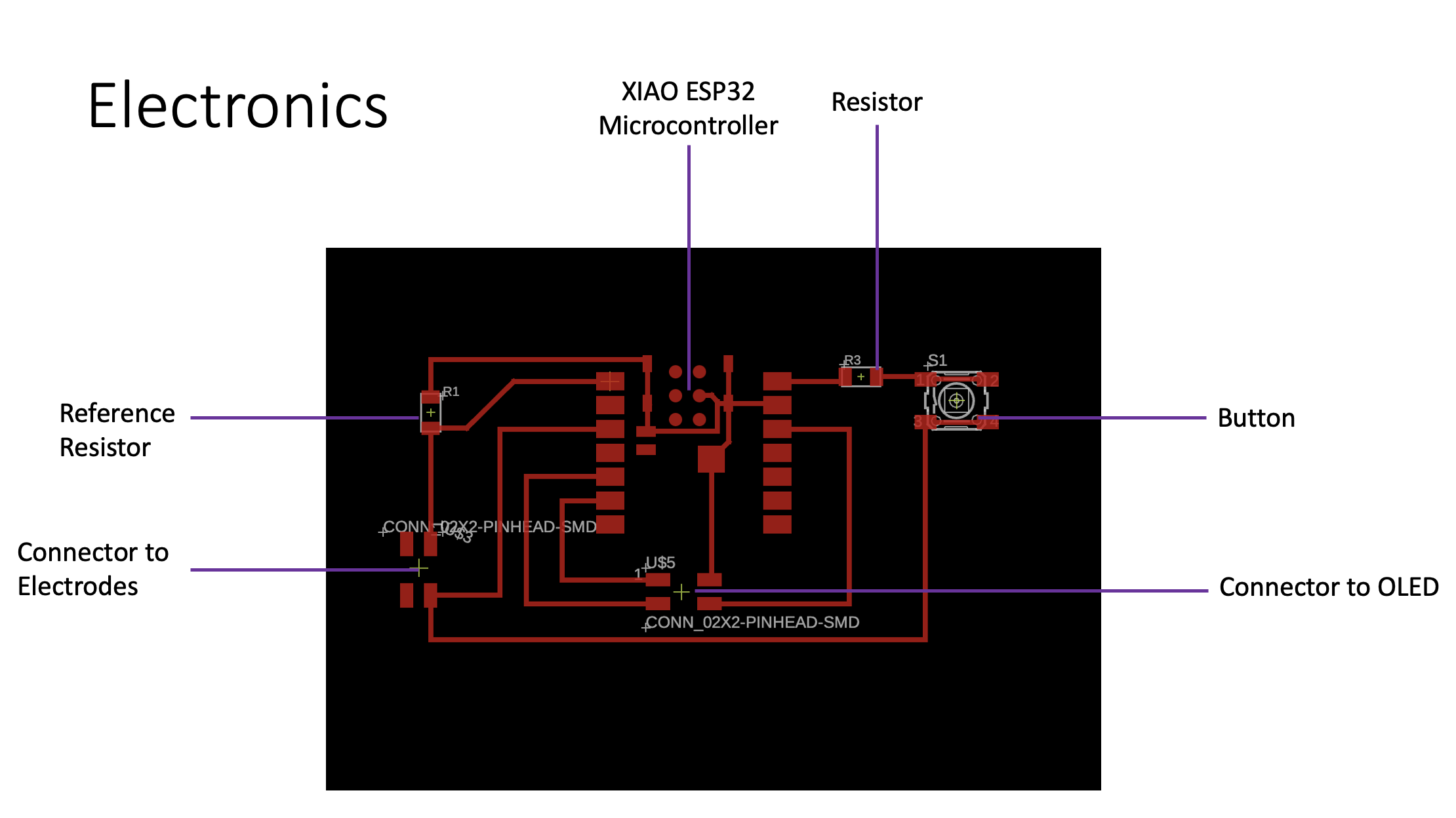
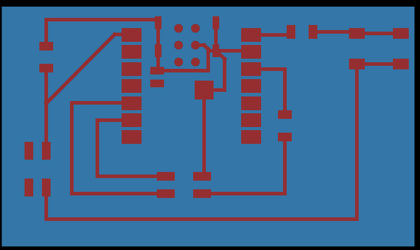
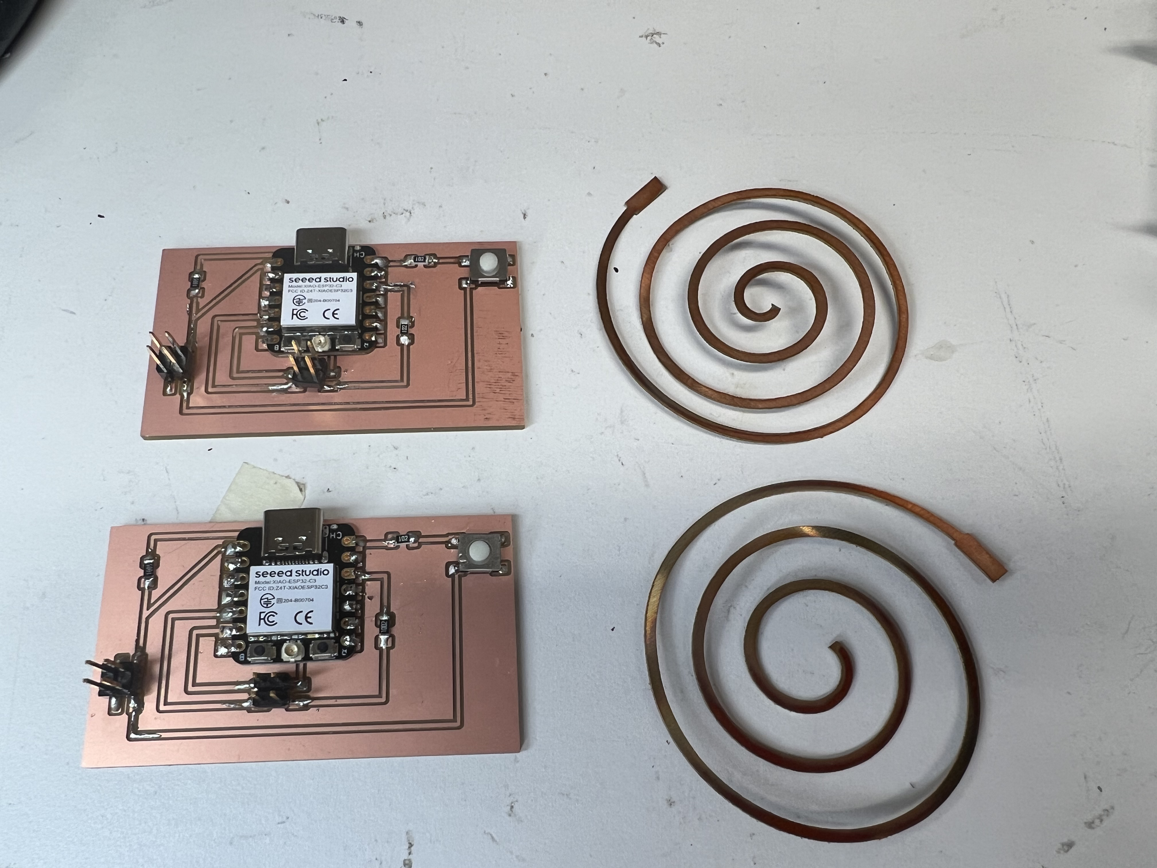
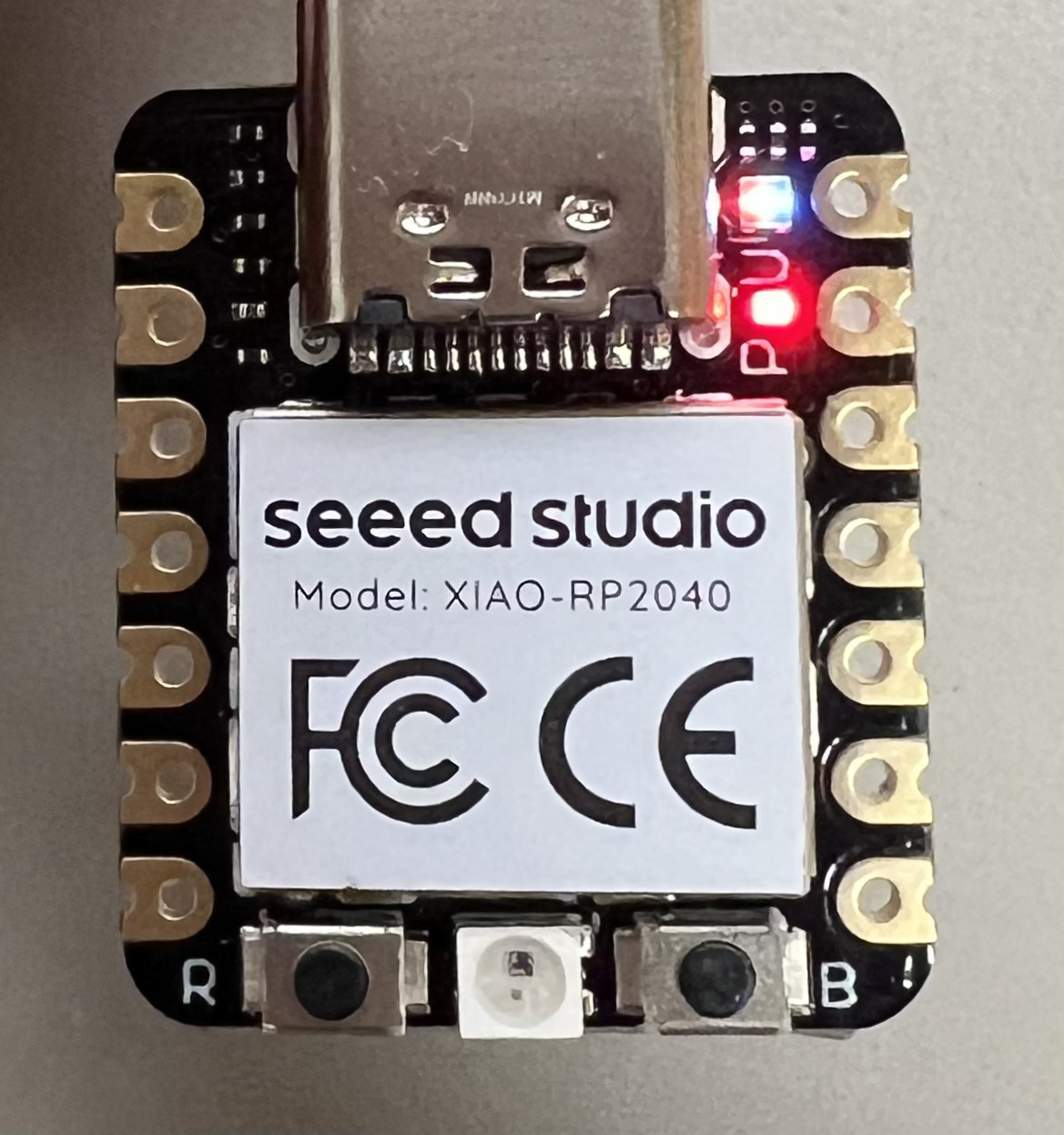
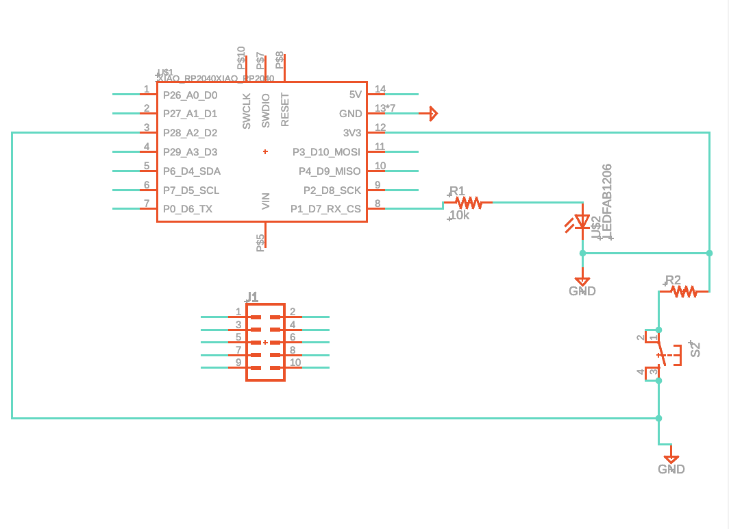
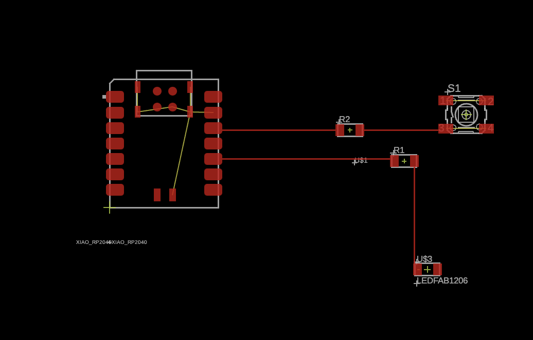
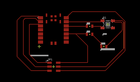
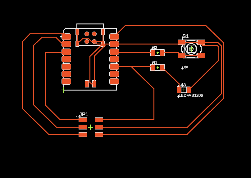
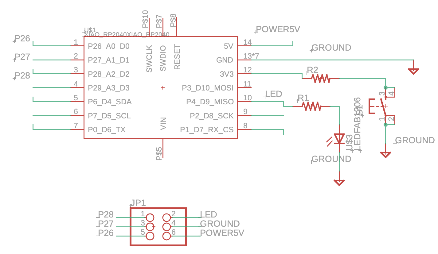
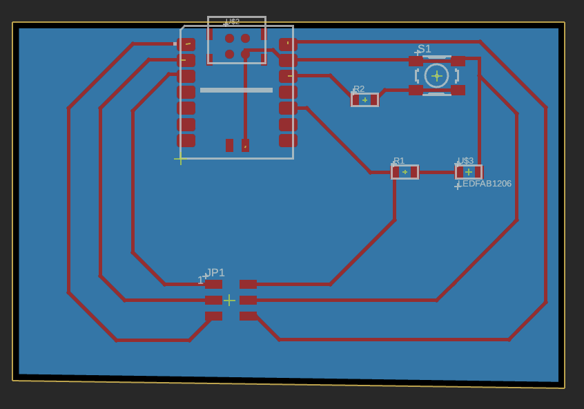
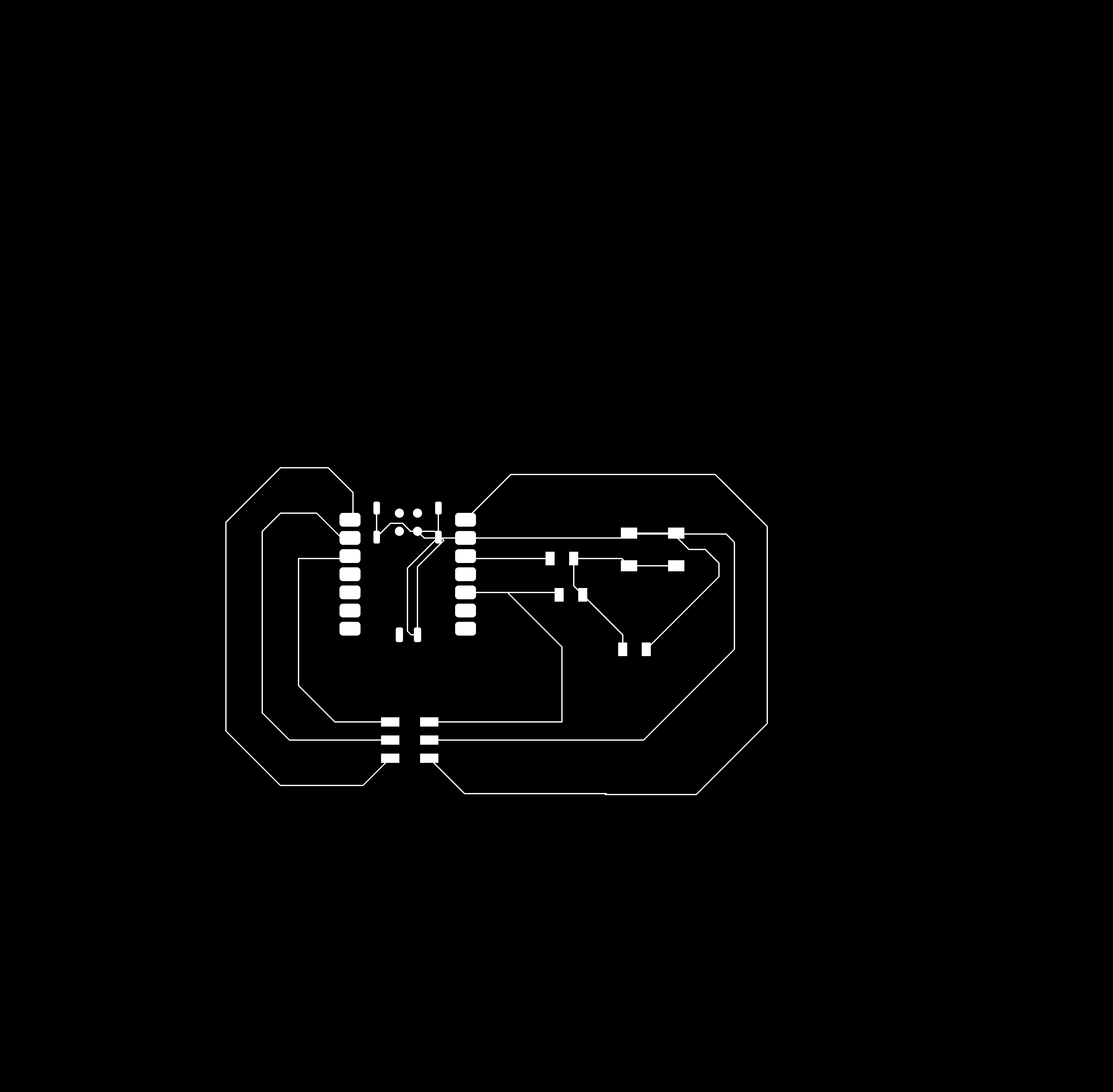
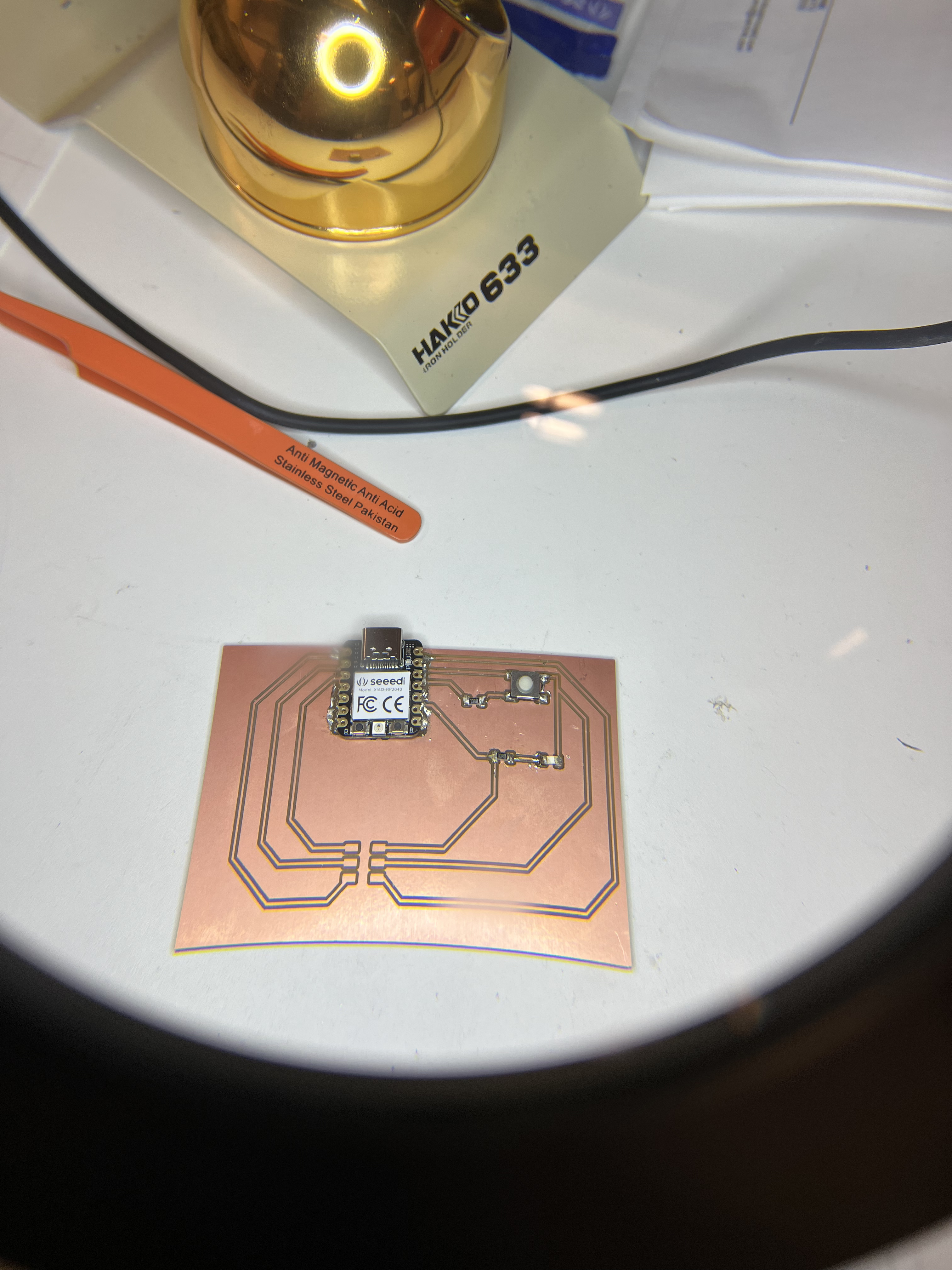
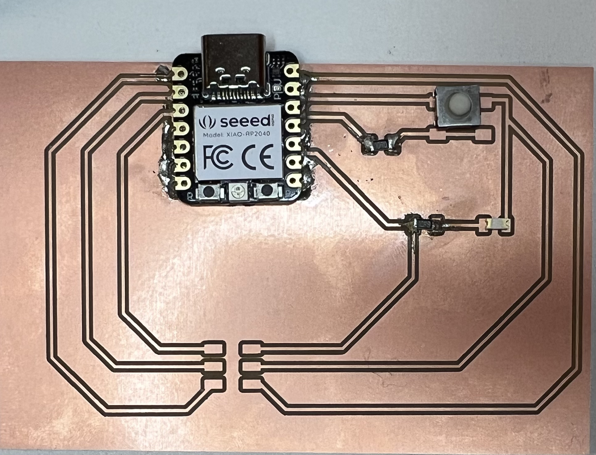
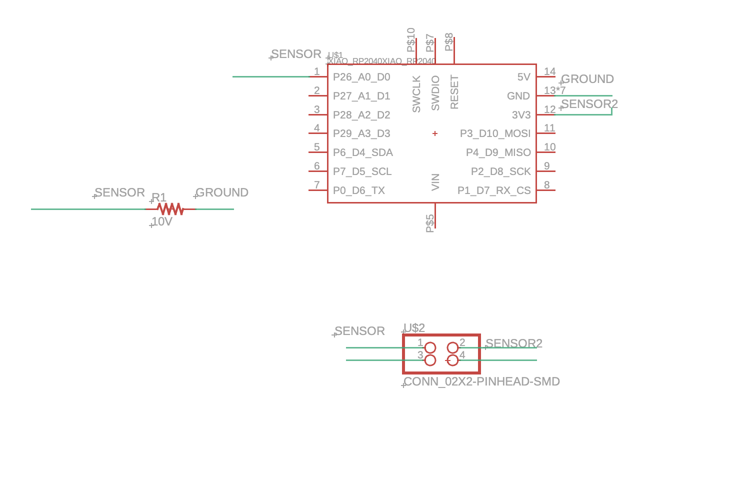
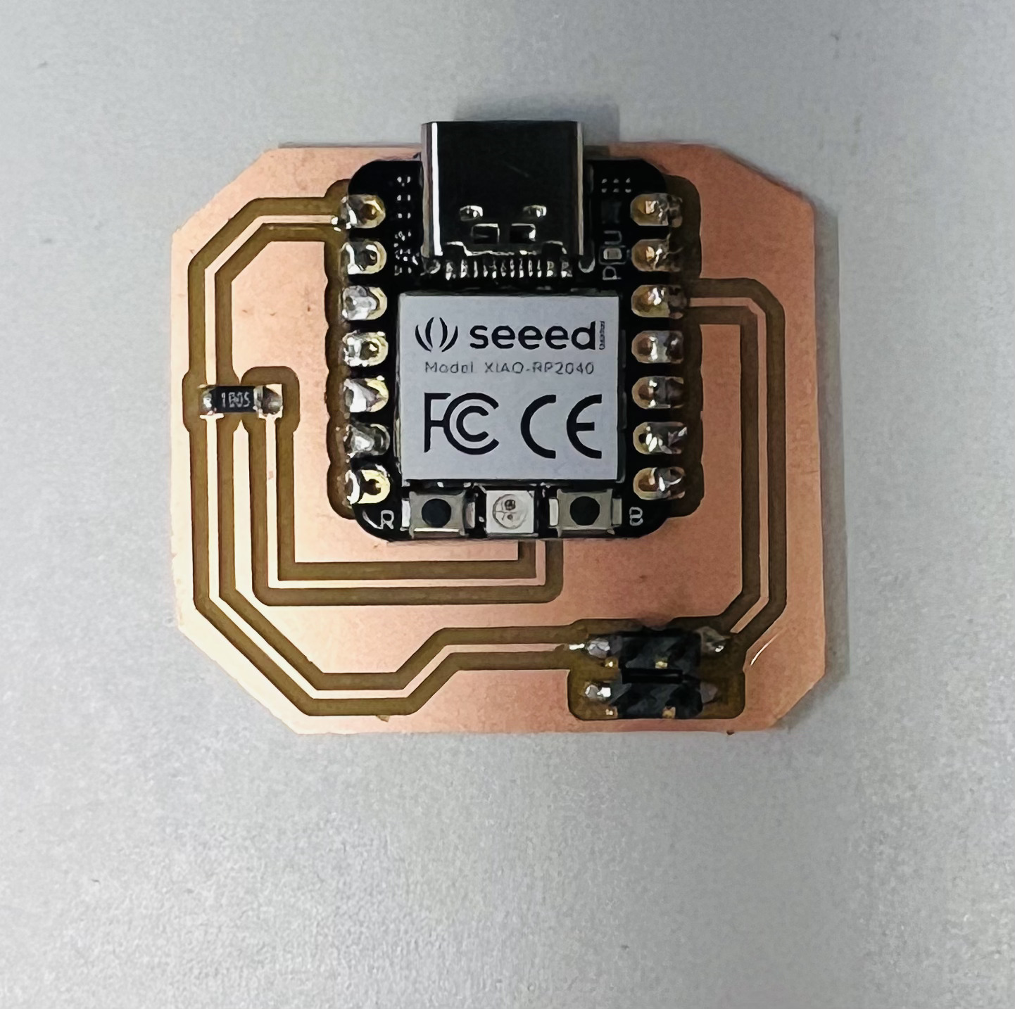
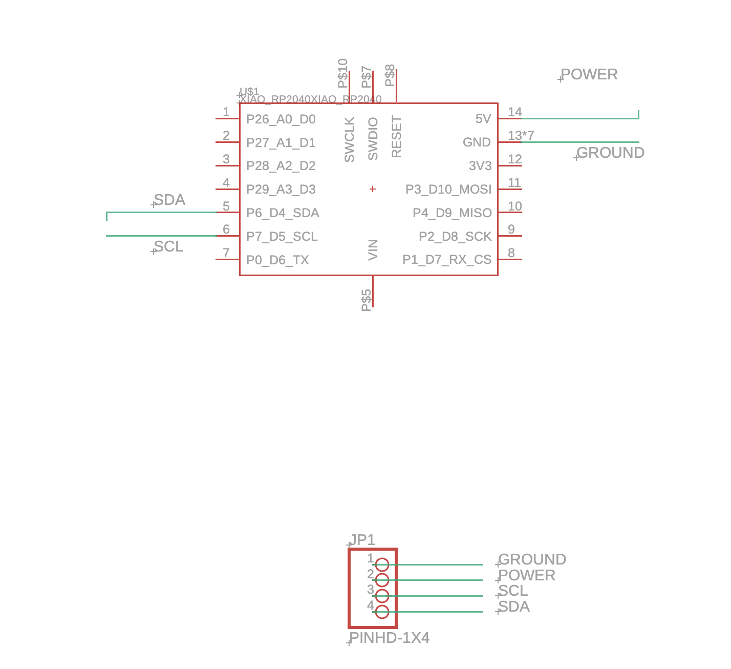
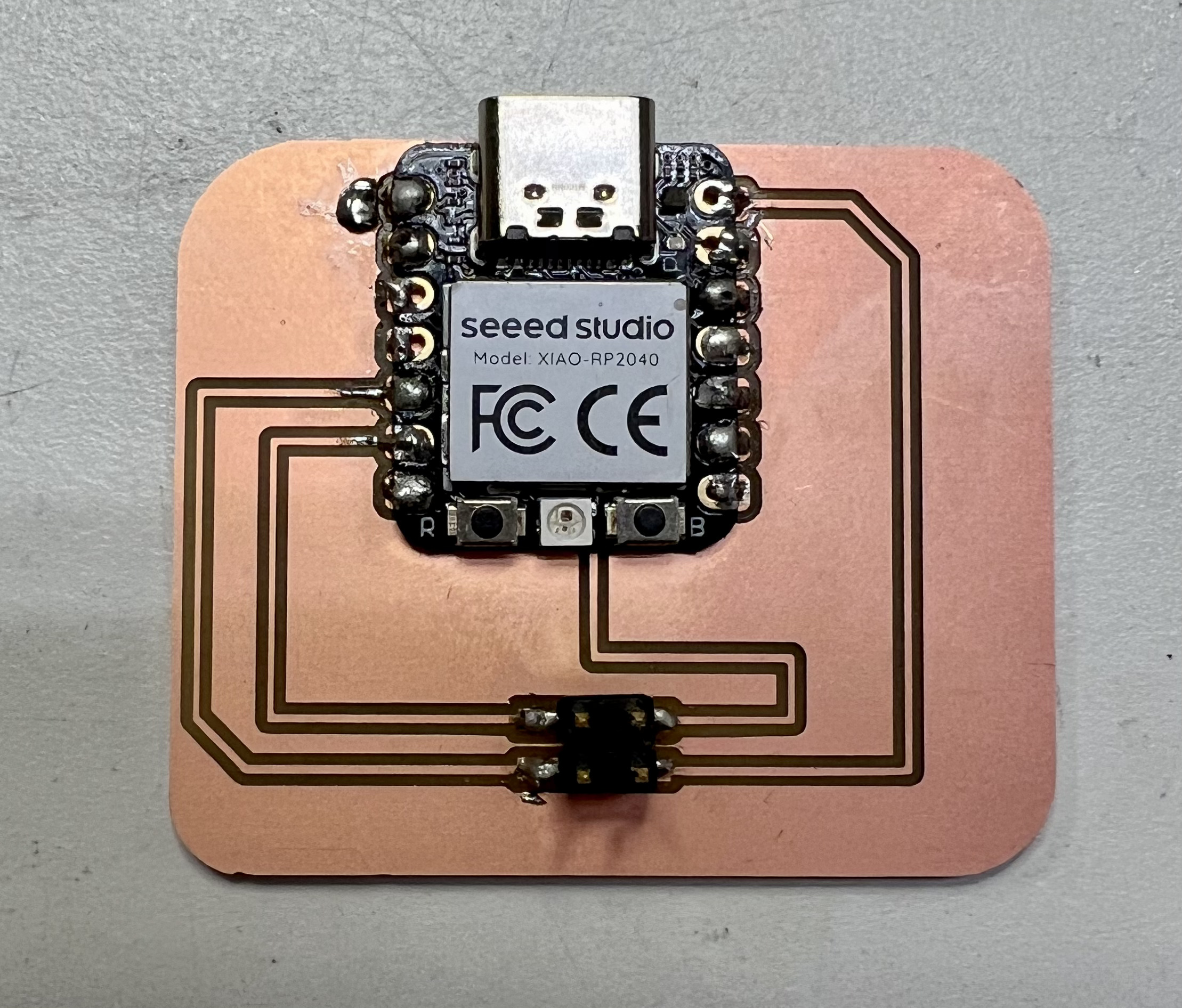
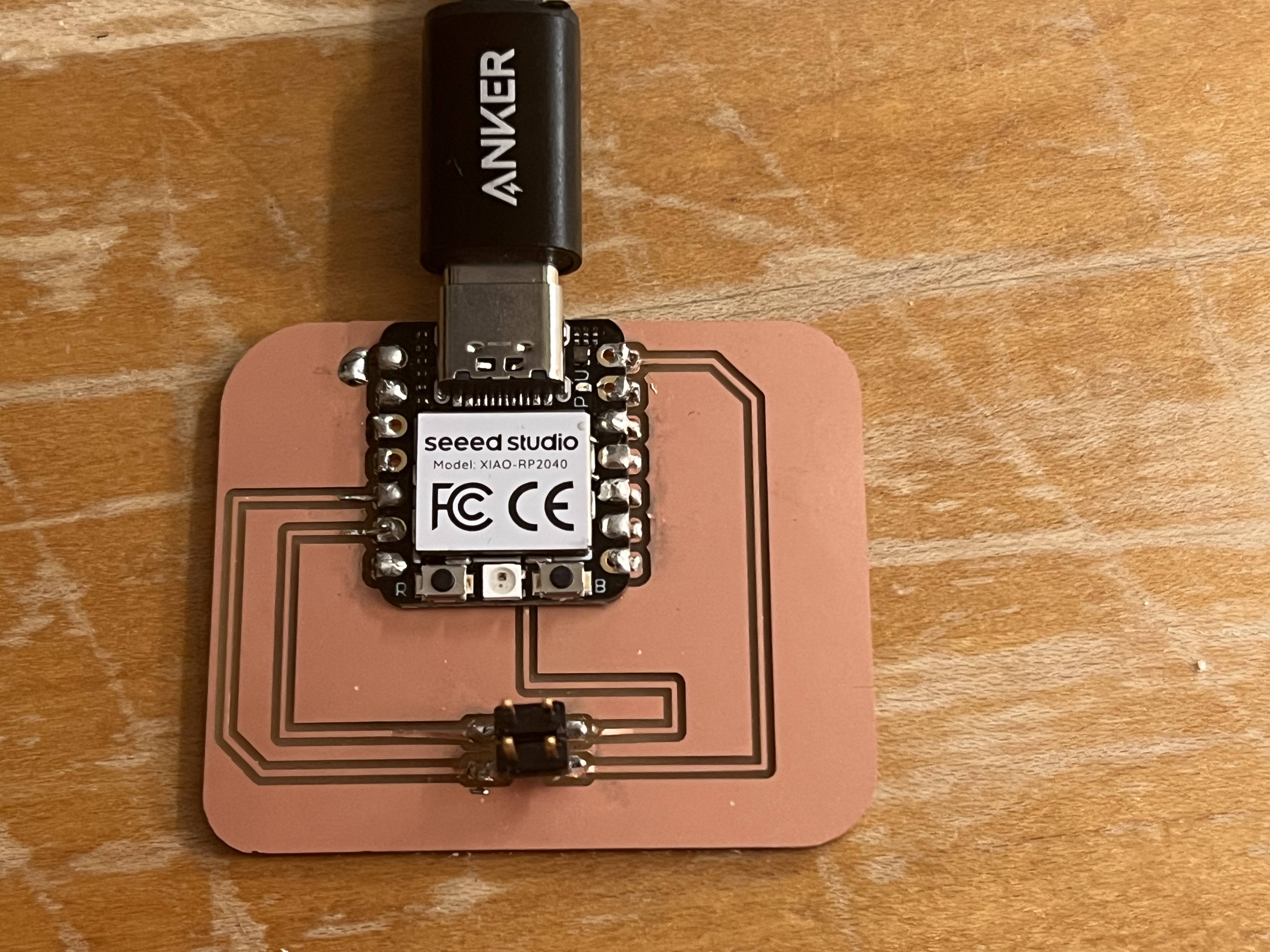
In the electronics sphere, I aimed to target resistance measurements of PFAS over time. In order to achieve this, I employed a voltage divider with a 10M Ohm Reference resistor, which encouraged the real-time monitoring of the resistance of the polymer coatings. In addition, I targeted an XIAO-ESP32C3 microcontroller in order to further allow for wireless readout of PFAS concentration to users through a separate user interface. I also targeted an SMD-1306 OLED display in order to display the PFAS concentration with a button for further control of when the resistance measurements are taking place. In addition, the PCB board consisted of two 2x2 pin connectors for connections to the electrodes and the OLED display screen.
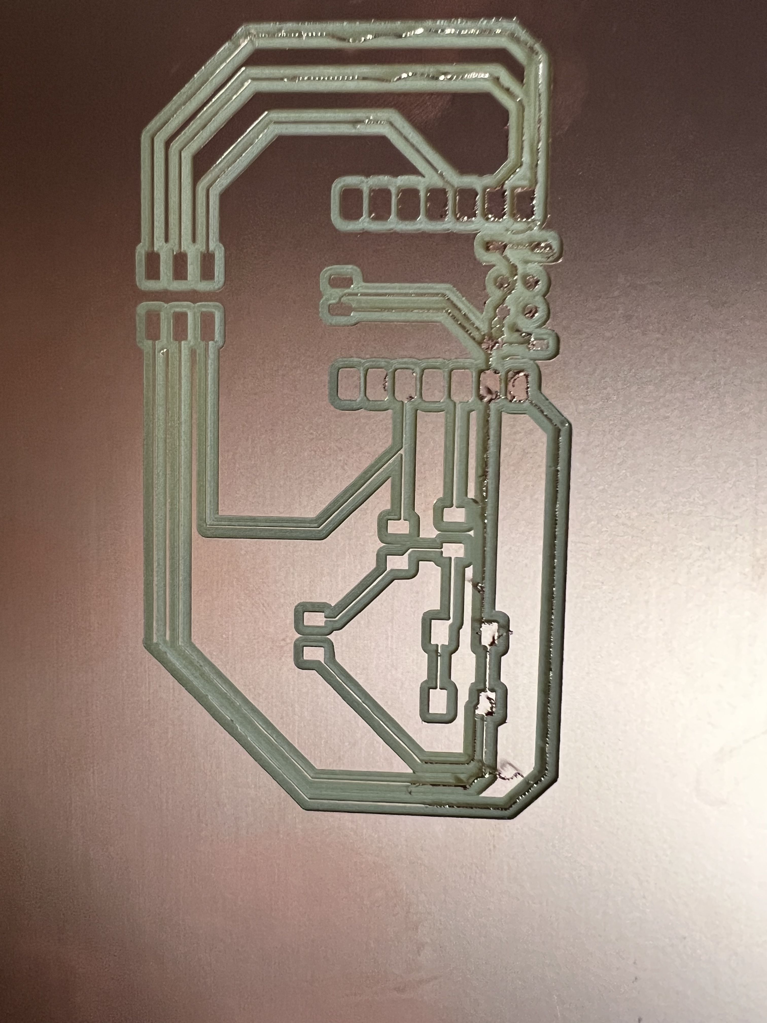
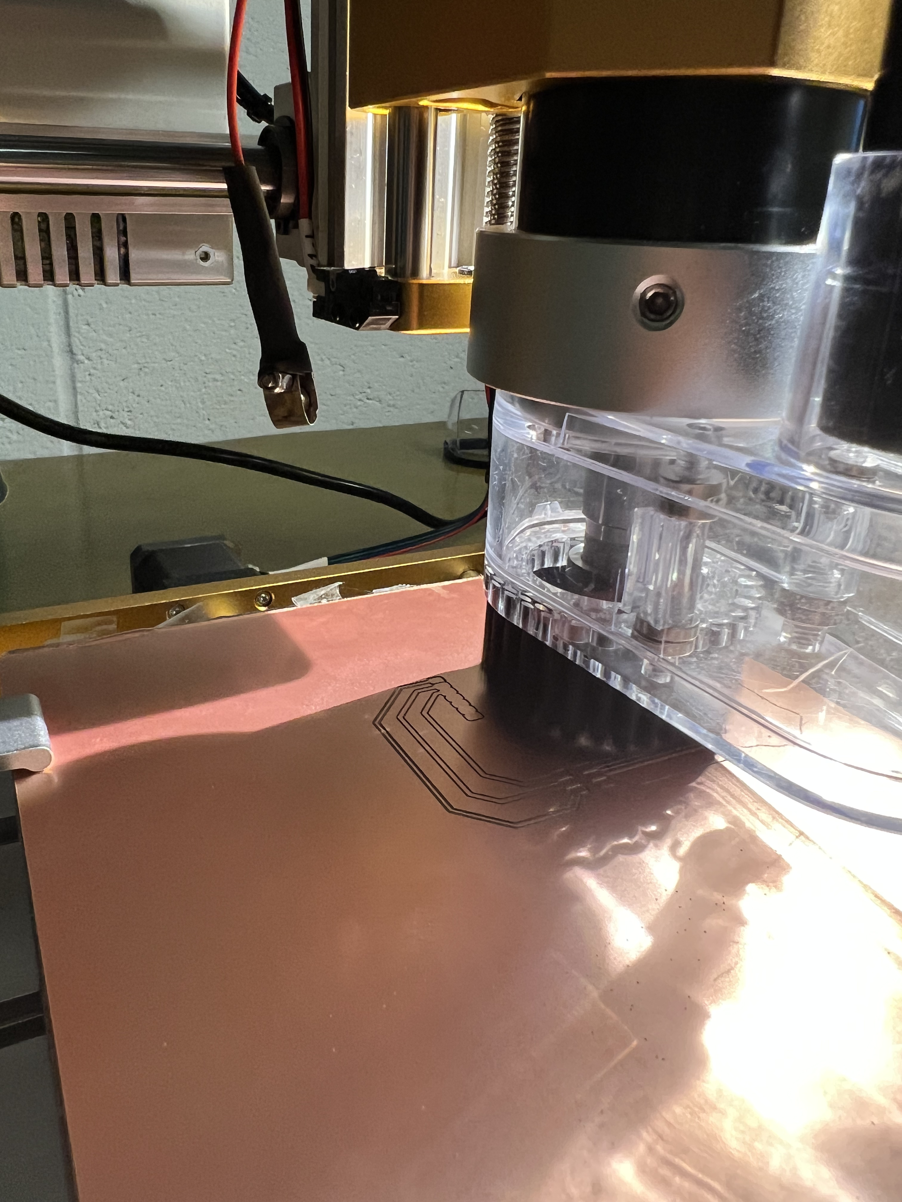
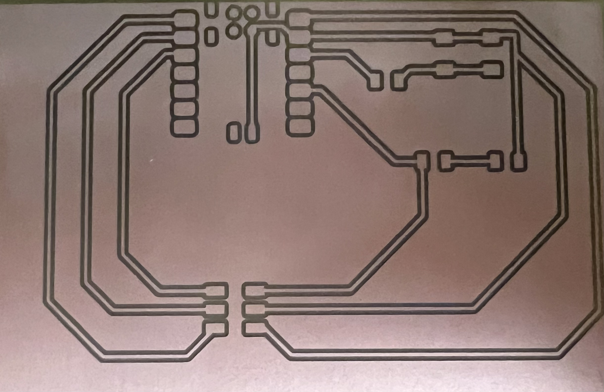
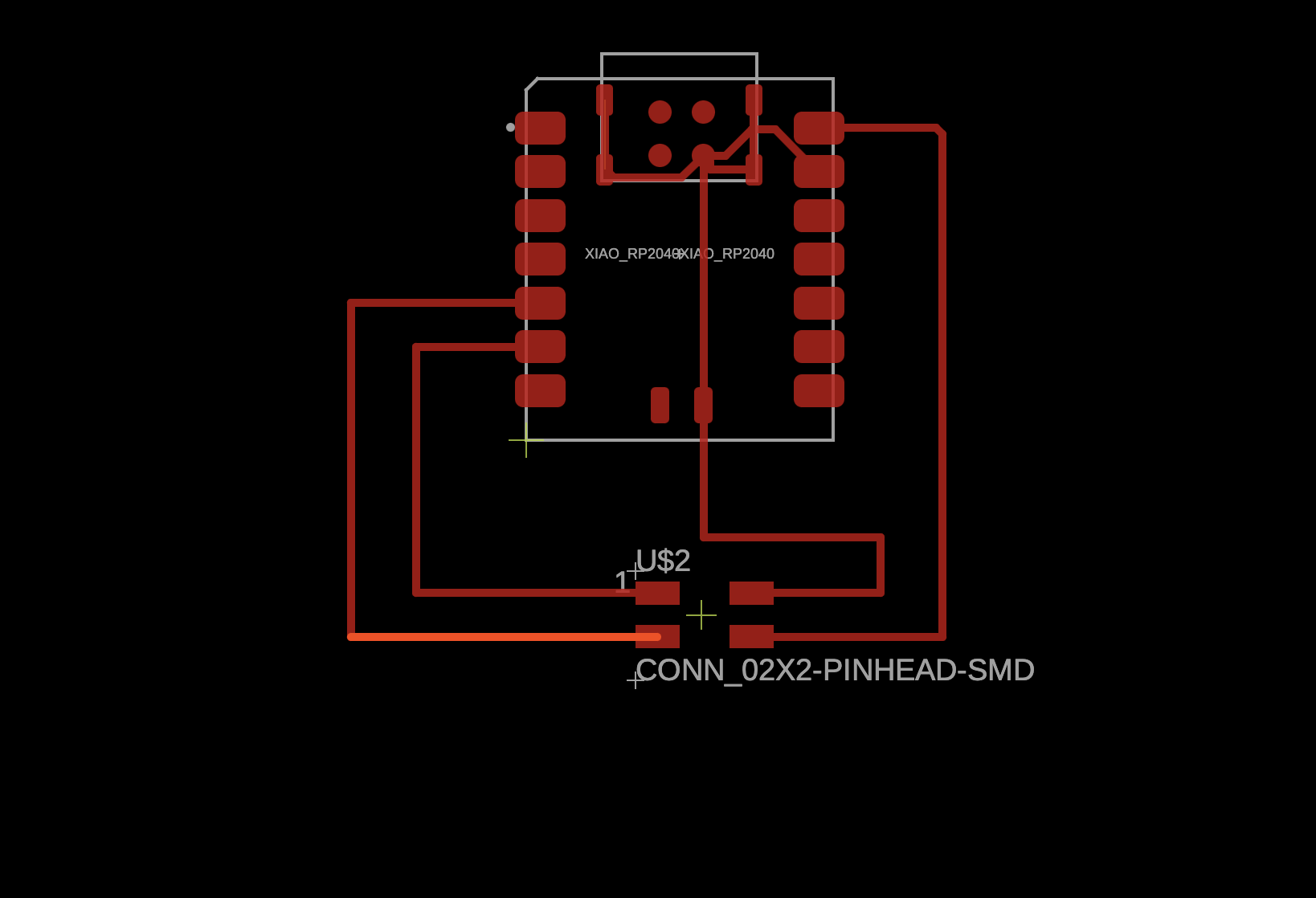
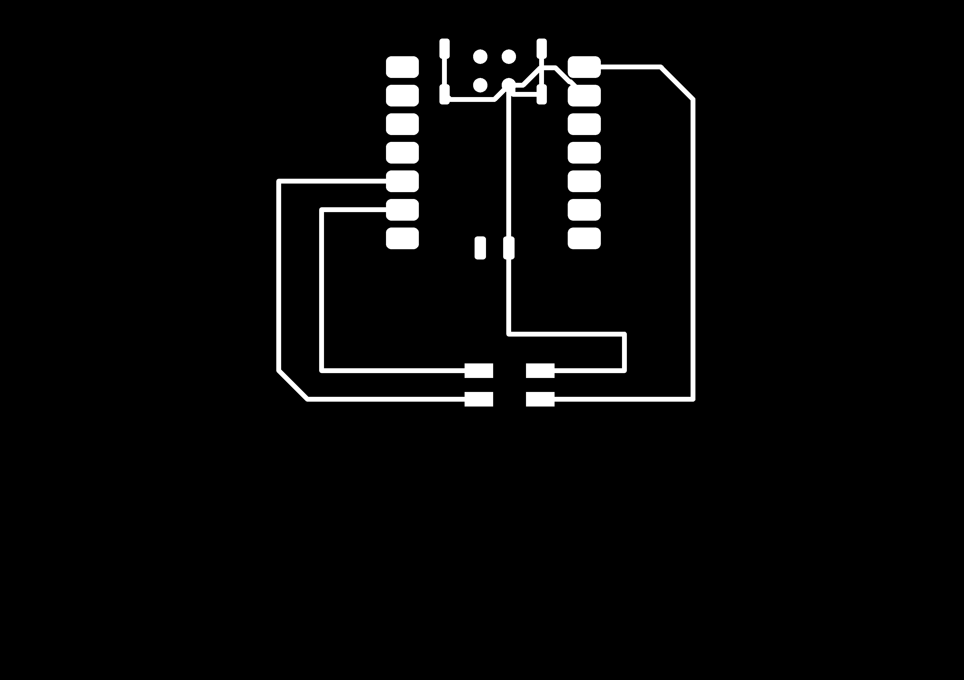
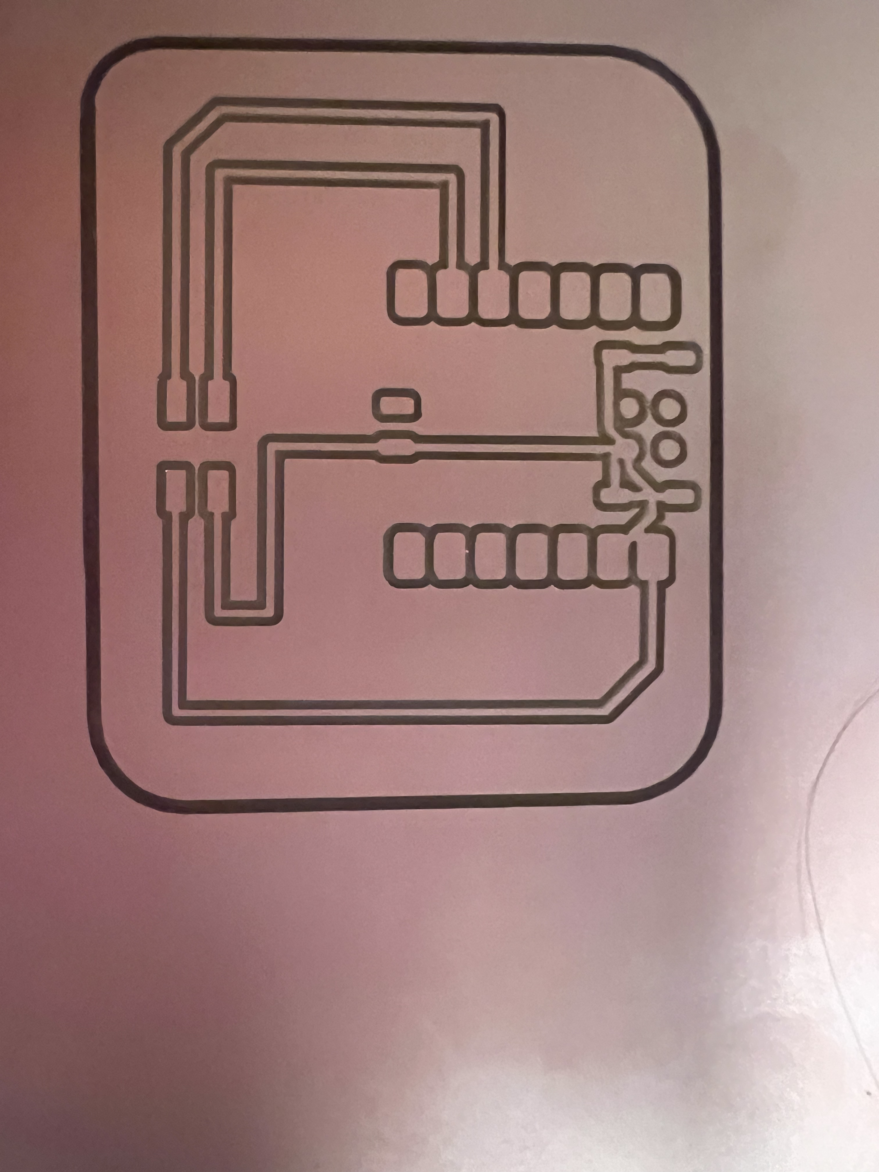
Upon designing my PCB board schematic drawing below, I extended the PCB board design in Fusion 360. Furthermore, I continued on to mill my PCB board after generating the g-code in MODS. Since I am interested in targeting the electronics of two devices, I aimed to mill two PCB boards. During the milling process, I unfortunately got hurt and had to take some time to recover my hand. (Real blood, sweat, and tears were unfortunately invested in the project.)
From here, I went on to solder my components onto the board with a tin-metal alloy. After a plethora of boards milled over the semester, I am happy to say that my soldering skill flow finally came into full bloom, which was very helpful for the final design.
Electrode Design
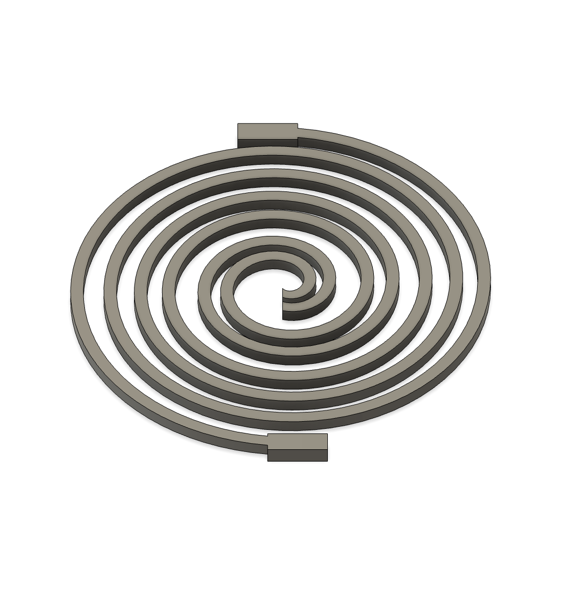
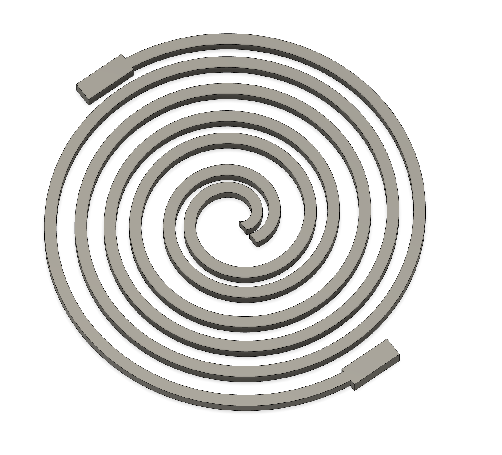
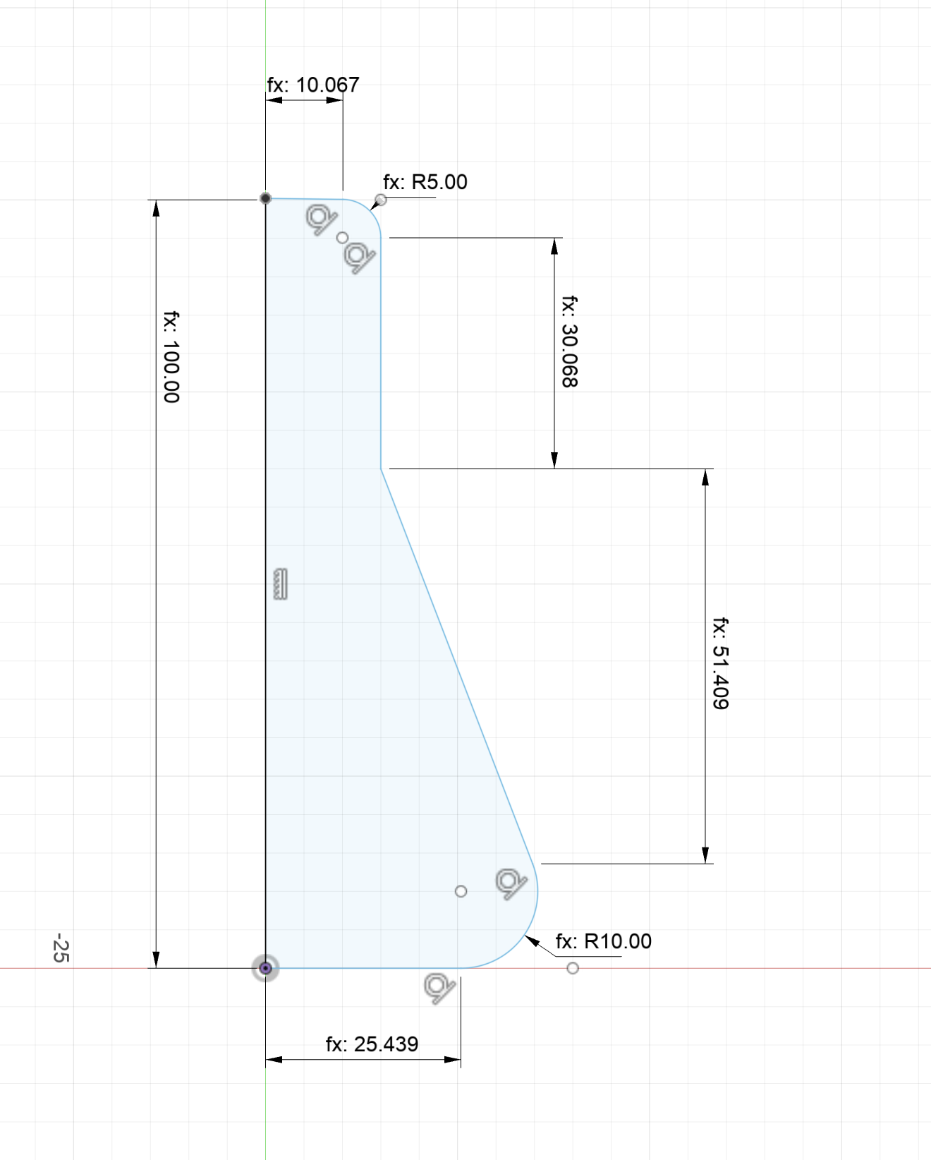
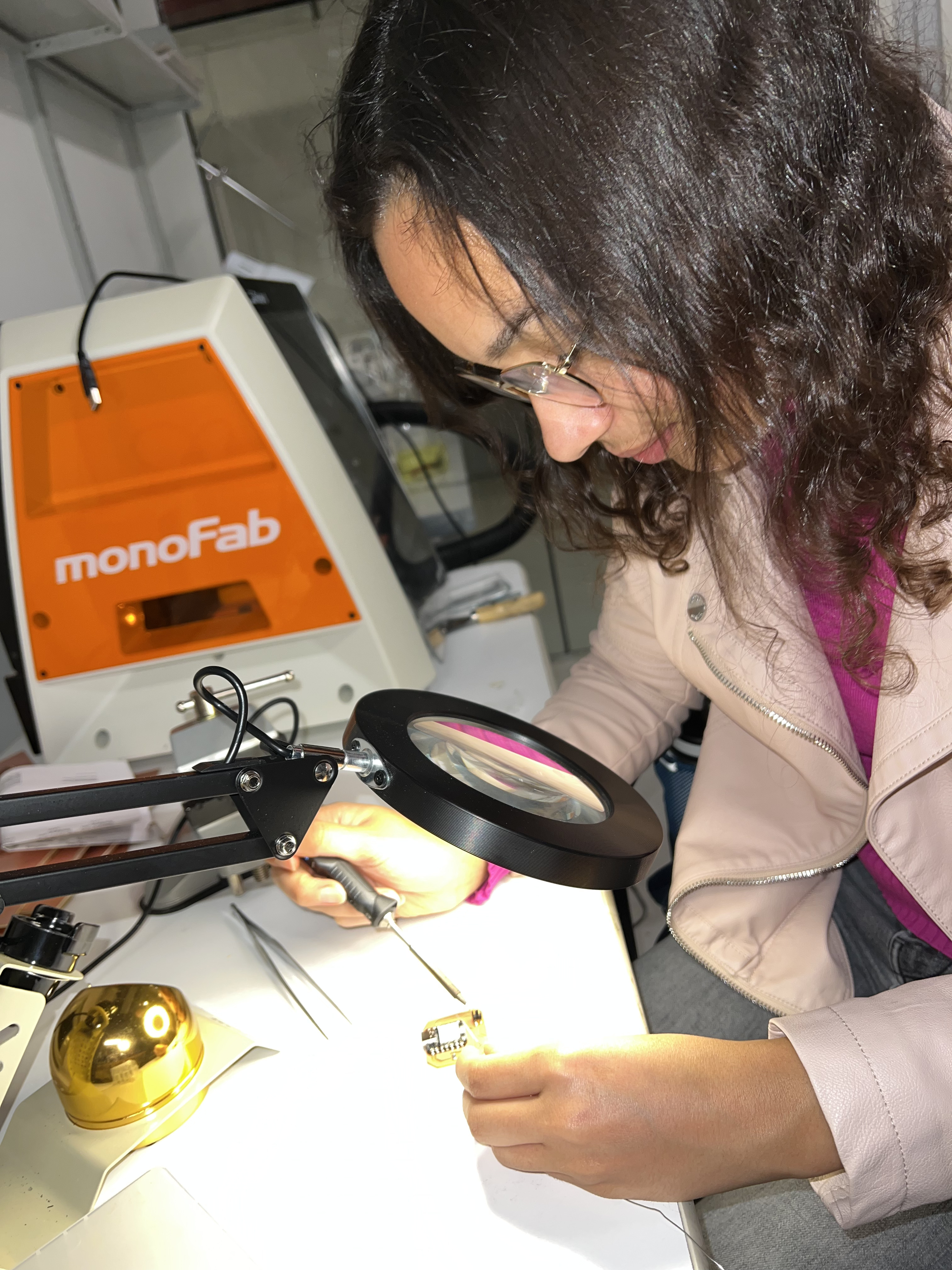
With the goal of maximizing the surface area contact of the copper electrode and the polymer filter paper films, a spiral-like electrode design was targeted in Fusion 360 Software, by employing the spiral design feature. Moreover, with this design, it was of interest to incorporate a spiral design of the copper electrodes. With this, the diameter of the spiral electrodes was parameterized to be equivalent to 55 cm (the diameter of the cellulosic paper coated with PANI polymer. The electrodes for the lateral flow assays were laser cut as well, with 3 mm x 2mm dimensions. From here I went on to laser cut the copper sheets with Alfonso. Unfortunately, the copper electrode cuts fell beneath the sides of the slits of the laser cutter. From here, I proposed to add a backing to the copper sheet in order to prevent the copper pieces from falling. This proved to substantially help. Then, I soldered the electrodes onto connecting chords with tin and a soldering iron. Thank you to Alfonso for your guidance with laser-cutting the electrodes!
Programming
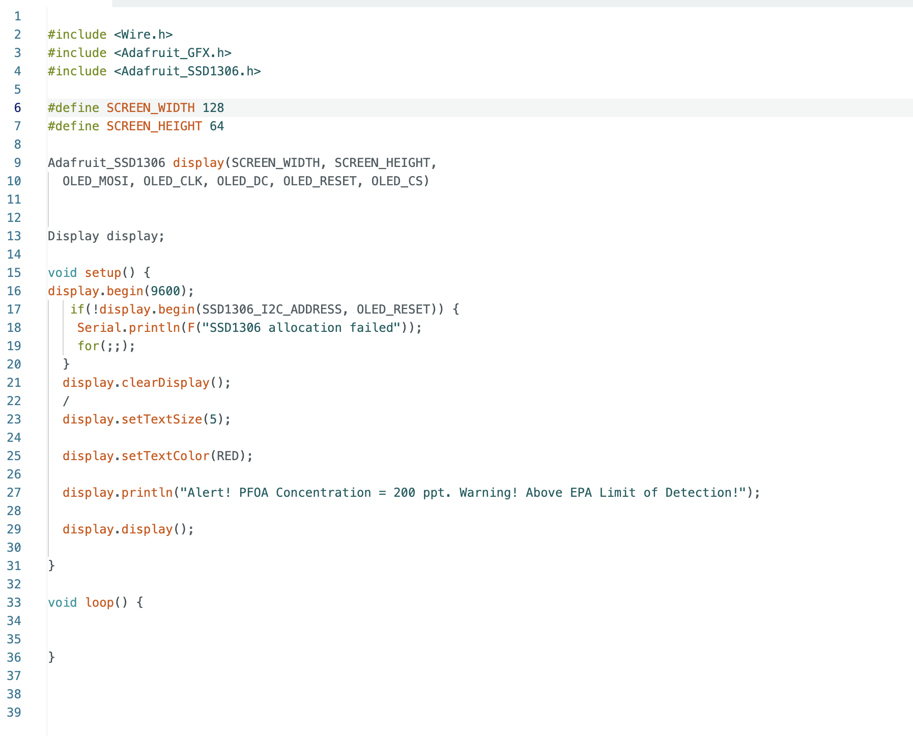
In order to program the microcontroller to monitor the resistance over time, I employed Arduino ID with C++ programming language. As an SD-1306 OLED Screen was employed, it was necessary to first download the library of the OLED screen on Arduino IDE before beginning to code. The following lines of code were developed for OLED screen readout:
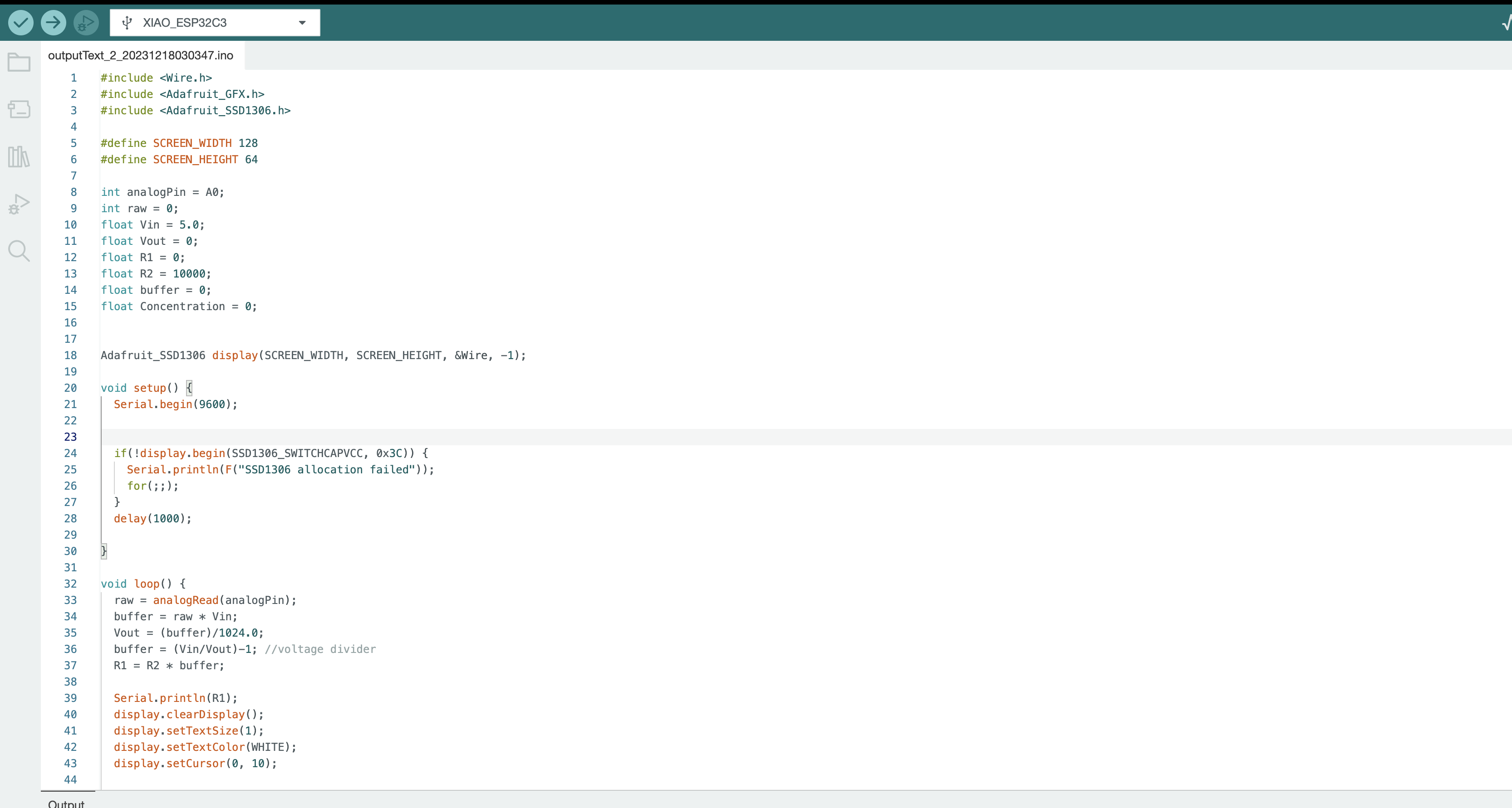
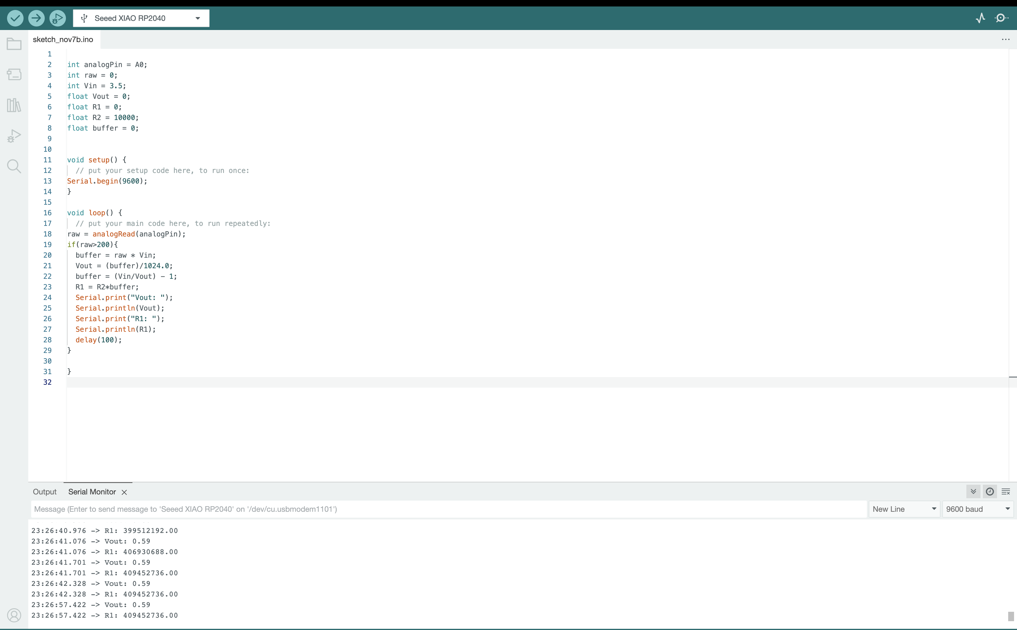
I employed a voltage divider in order to encourage the measurements of the resistance between the electrodes with reference to a 10MOhm resistor. Thus, the equation for the voltage divider was the following:
buffer = raw * Vin;
Vout = (buffer)/1024.0;
buffer = (Vin/Vout)-1; //voltage divider
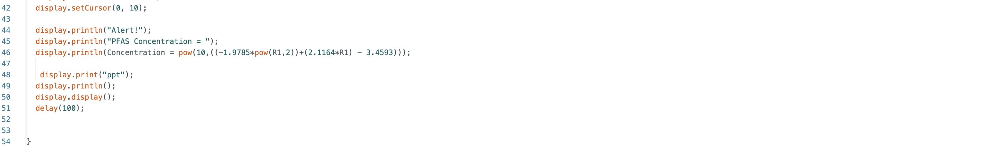
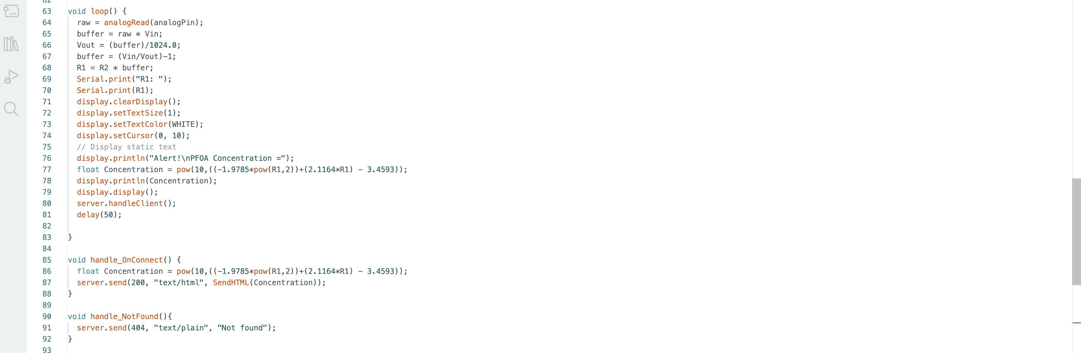
In addition, as I was interested in converting the measured resistance to the concentration of PFAS, I employed the equation for the concentration of PFOA with respect to the resistance, referencing previous PFOA studies carried out with PANI coatings and PFOA. This encouraged me to gain further insight into back-calculating the concentration of PFOA as the resistance of the PANI coatings changes with exposure to PFAS.
The following lines of code were developed:
Networking, Communications, and Interface
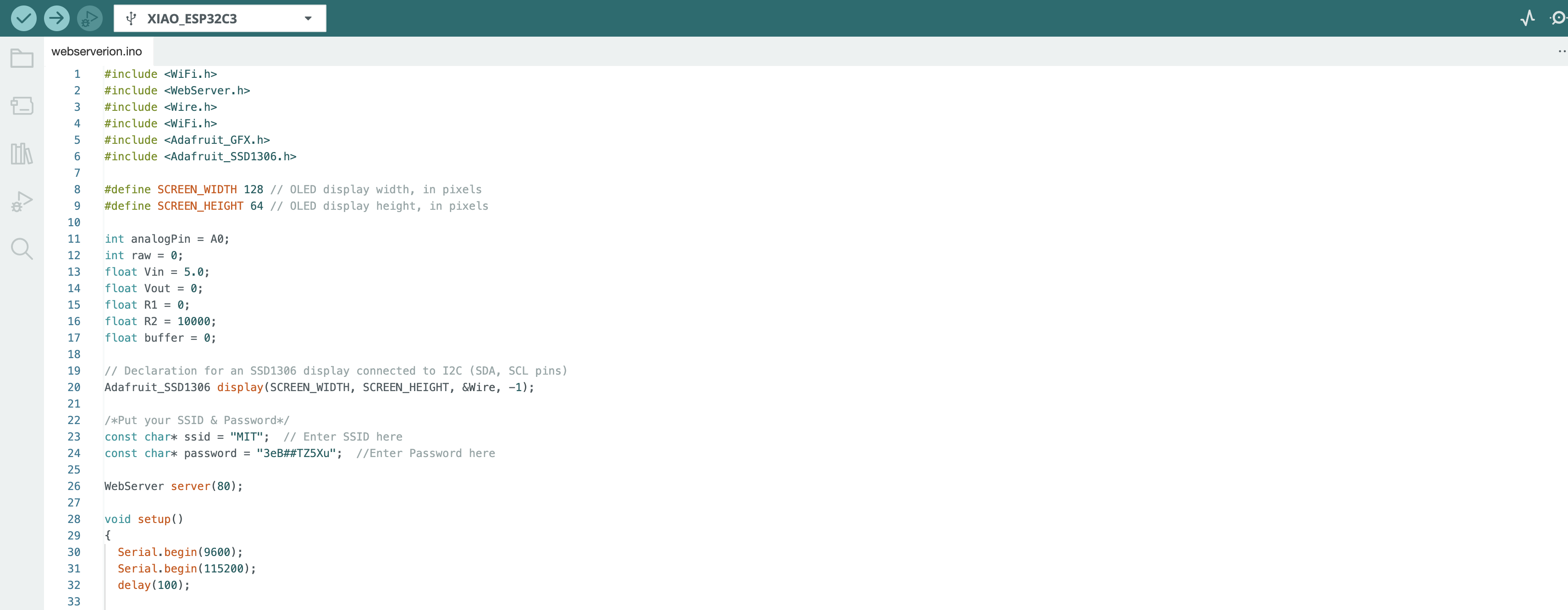
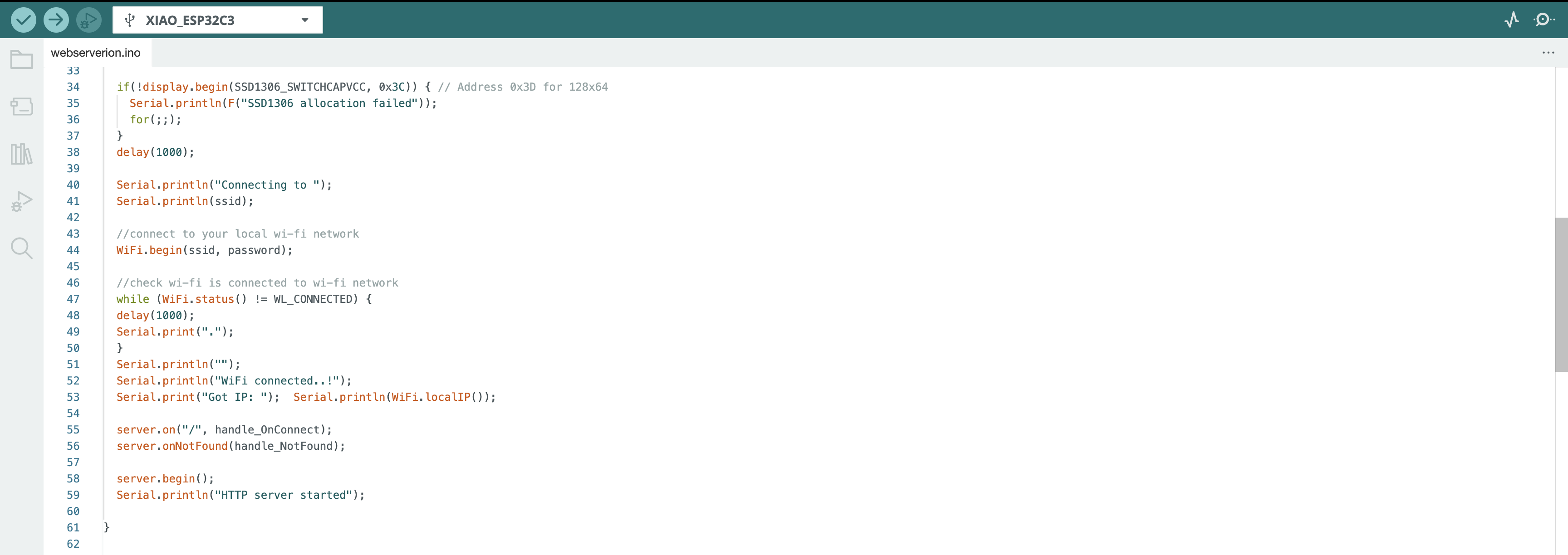
For the final project, I chose to expand my usual spotlight on the XIAO-RP2040 Microcontroller to the XIAO ESP32-C3 Microcontroller. The beauty behind the ESP32 is that it encourages both bluetooth and wifi connection, which is ideal for communicating the PFOA concentration with users for my final project device. Moreover, both the wifi and bluetooth communication are long range, which encourage expanded communication.
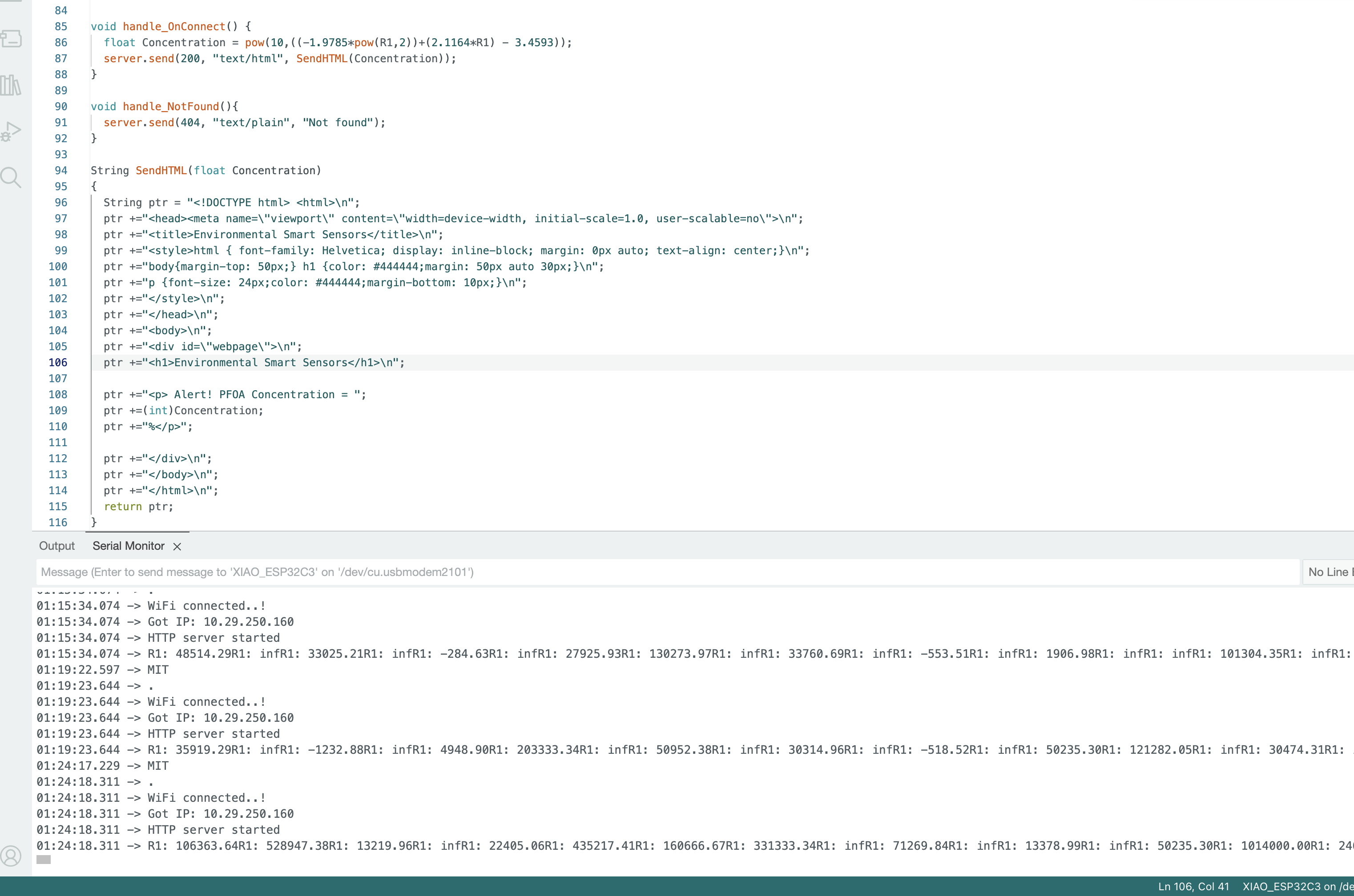
For the final project, I targeted a wifi readout of the PFOA concentration in water, along with a user interface website generated. Particularly, I employed Arduino IDE with C++ programming for this. Particularly, I referenced to the following ESP32-C3 Wifi Usage code, https://how2electronics.com/getting-started-with-seeed-xiao-esp32-c3-board/ for inspiration. Significantly, I aimed to develop a web server with expanded connection to the SSD 1306 OLED Screen for continue sensing device readout. This encourages the target of both an output readout on the device along with a user interface through wireless connection.
It is important to note that in this case of sensing studies, the resistance of a polymer film was not measured, hence the resistance read 0 and the PFOA Concentration read 0. For further studies, I still continued to employ the voltage divider equation from prior sensing studies alongside the equation for the PFOA concentration from previous sensing studies.
Upon verifying and uploading the code, I yielded a wifi connection on the serial monitor, followed by a generated IP address. From here, I was able to further connect to the wifi on my phone and generate a user interface for the PFOA concentration readout, along with a readout on my computer.
This is quite a useful approach for further PFOA sensing readouts, which I hope to continue to explore in the future.
Networking, Communications, and User Interface
For the final project, I chose to expand my usual spotlight on the XIAO-RP2040 Microcontroller to the XIAO ESP32-C3 Microcontroller. The beauty behind the ESP32 is that it encourages both bluetooth and wifi connection, which is ideal for communicating the PFOA concentration with users for my final project device. Moreover, both the wifi and bluetooth communication are long range, which encourage expanded communication.
For the final project, I targeted a wifi readout of the PFOA concentration in water, along with a user interface website generated. Particularly, I employed Arduino IDE with C++ programming for this. Particularly, I referenced to the following ESP32-C3 Wifi Usage code, https://how2electronics.com/getting-started-with-seeed-xiao-esp32-c3-board/ for inspiration. Significantly, I aimed to develop a web server with expanded connection to the SSD 1306 OLED Screen for continue sensing device readout. This encourages the target of both an output readout on the device along with a user interface through wireless connection.
It is important to note that in this case of sensing studies, the resistance of a polymer film was not measured, hence the resistance read 0 and the PFOA Concentration read 0. For further studies, I still continued to employ the voltage divider equation from prior sensing studies alongside the equation for the PFOA concentration from previous sensing studies.
Upon verifying and uploading the code, I yielded a wifi connection on the serial monitor, followed by a generated IP address. From here, I was able to further connect to the wifi on my phone and generate a user interface for the PFOA concentration readout, along with a readout on my computer.
This is quite a useful approach for further PFOA sensing readouts, which I hope to continue to explore in the future.

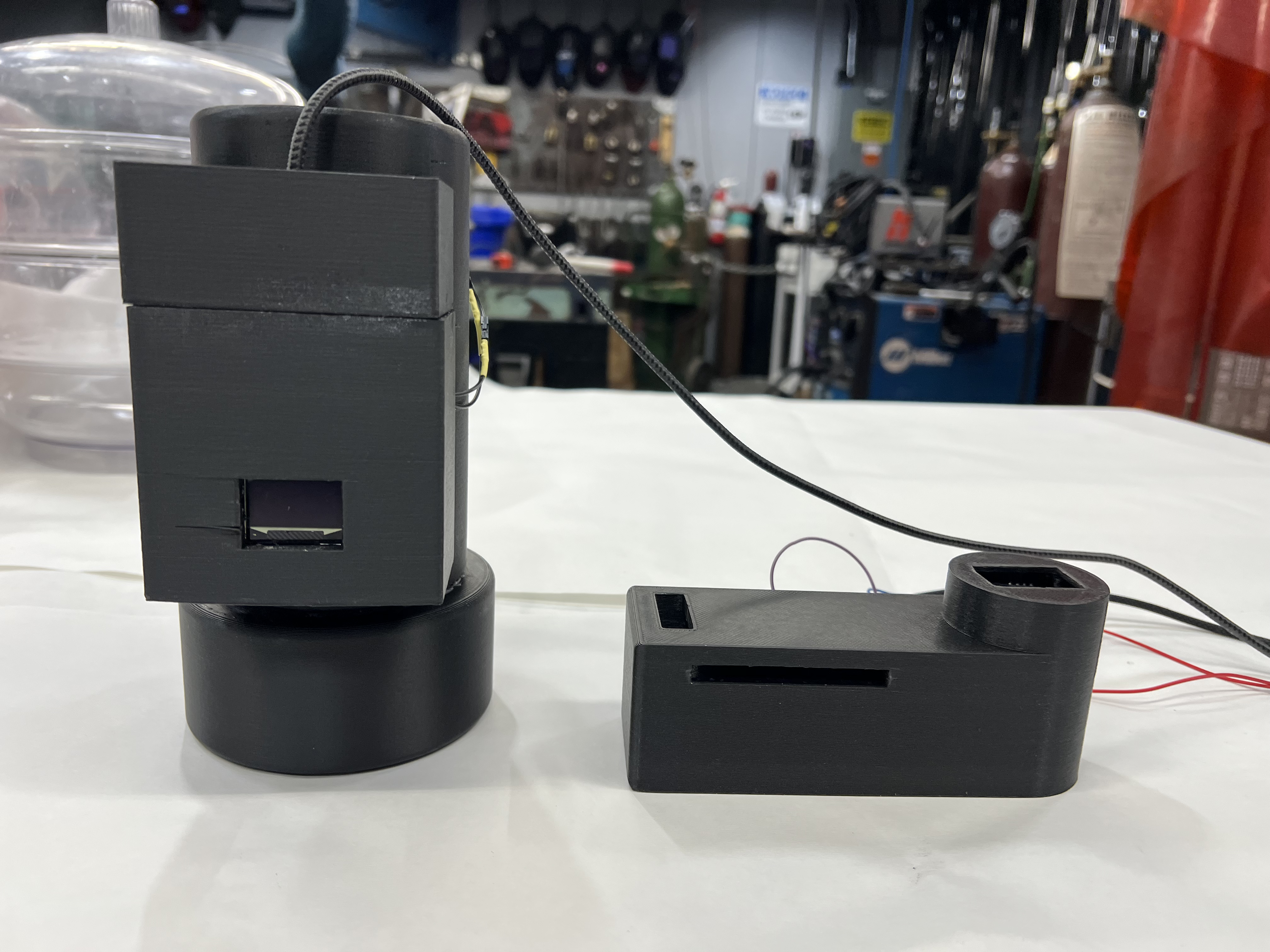
Design and 3D Printing
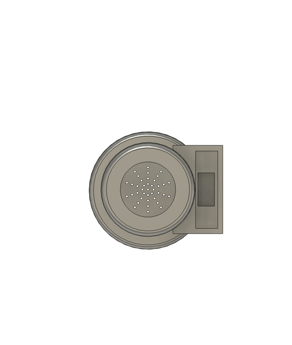
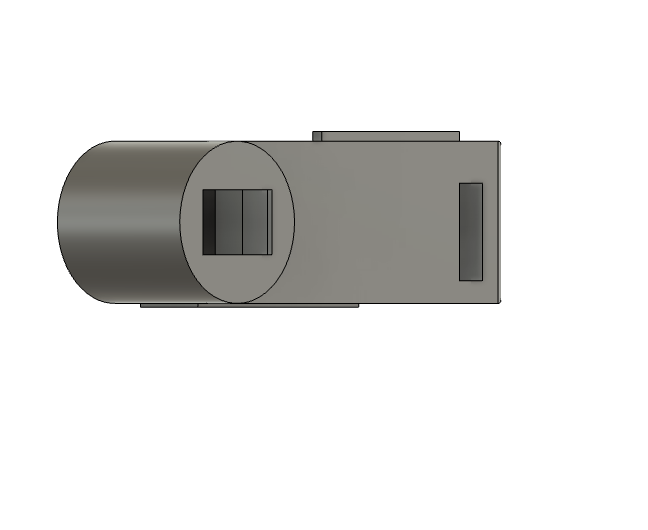
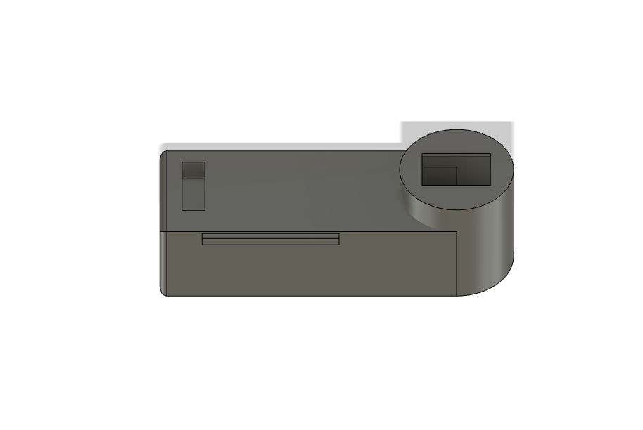
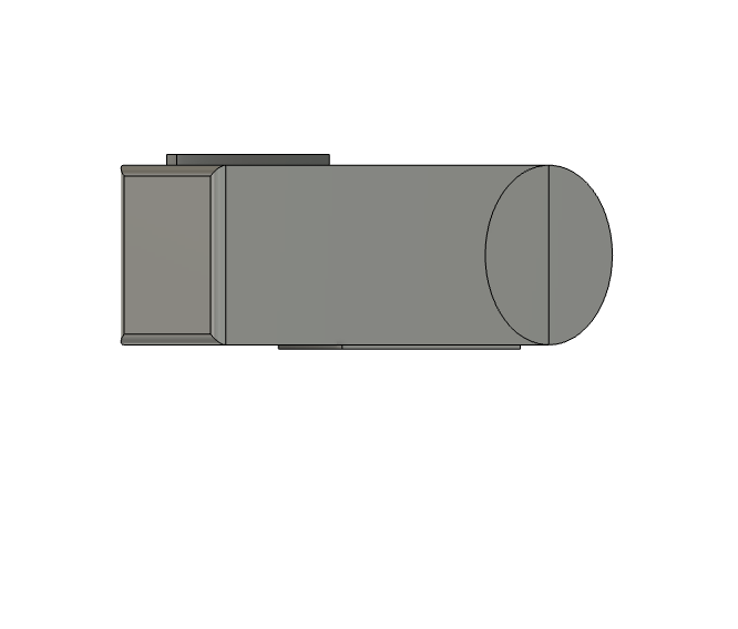
Smart Filter
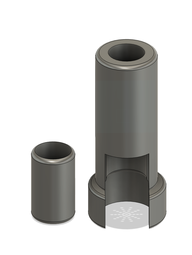
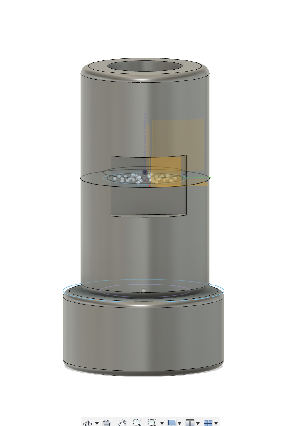
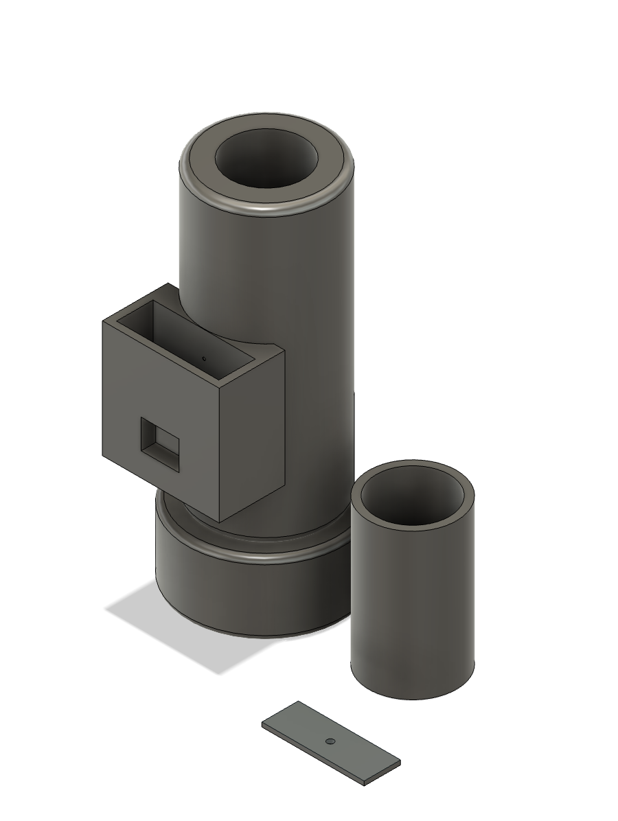
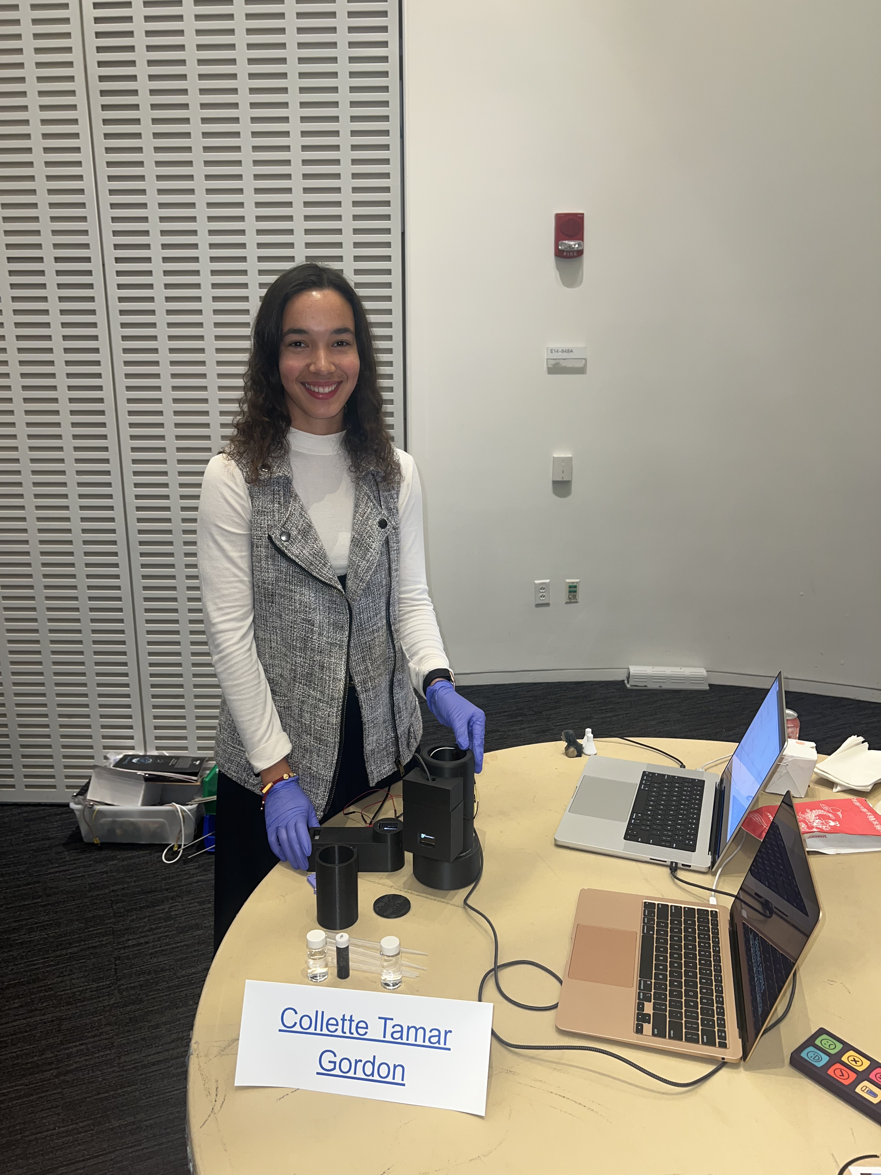
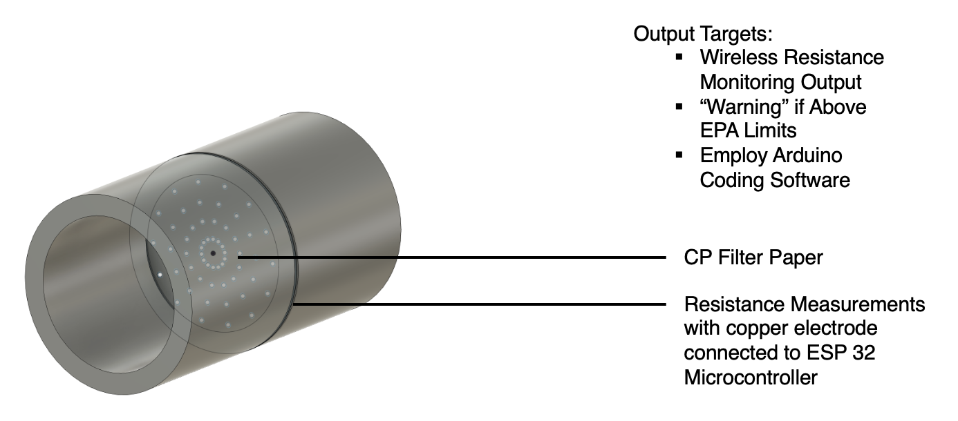
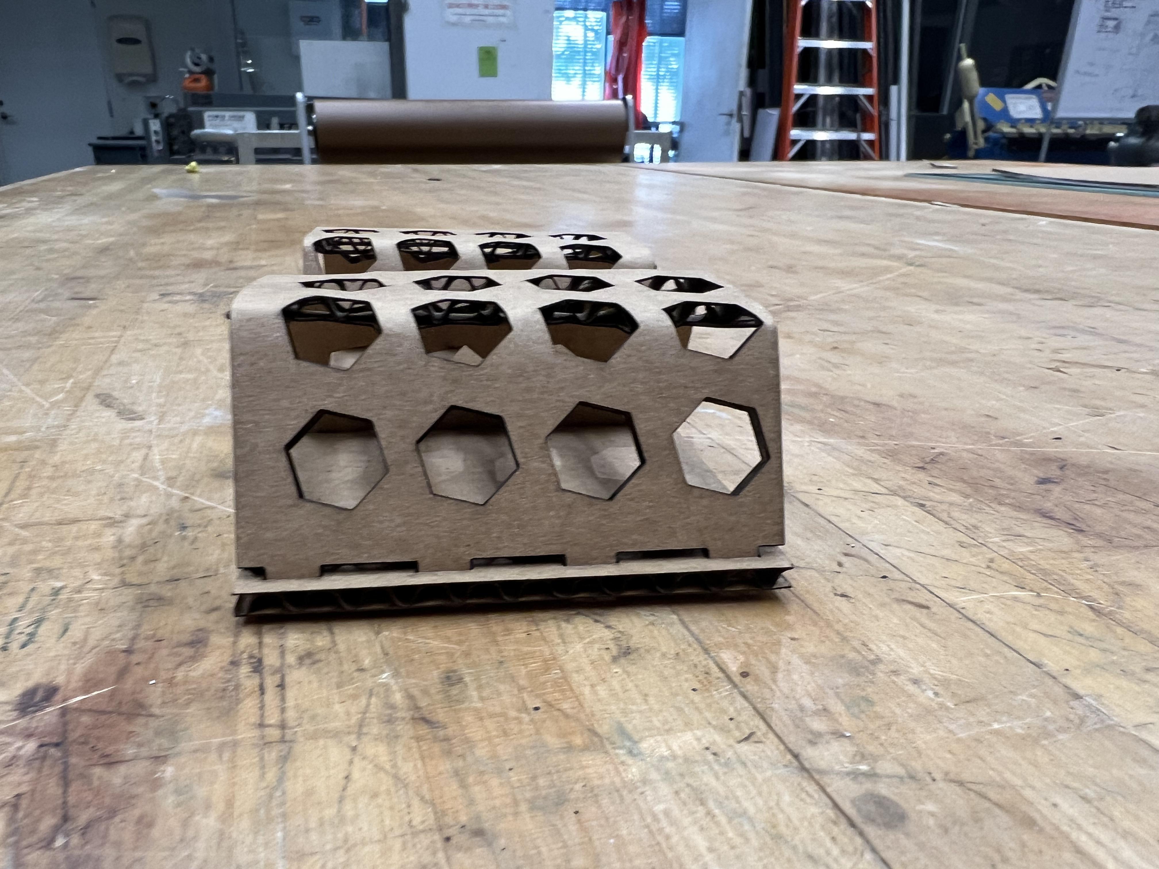
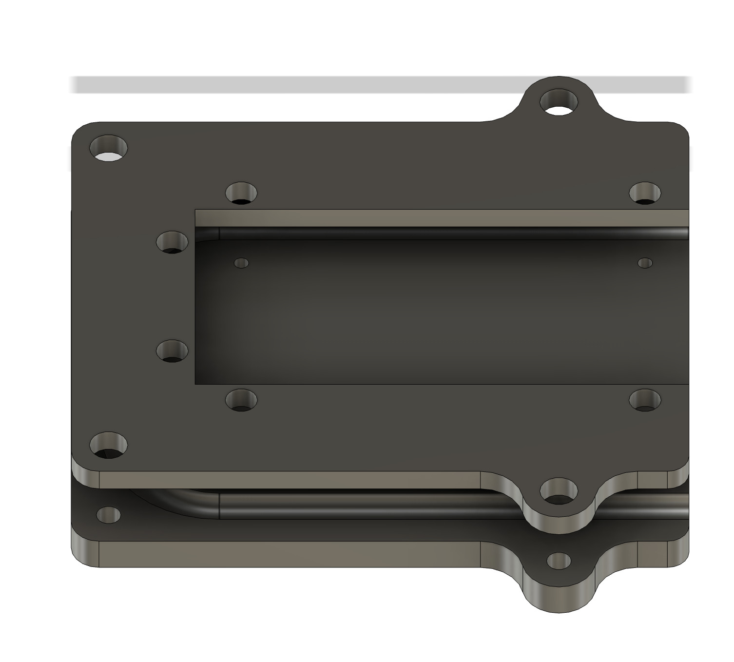
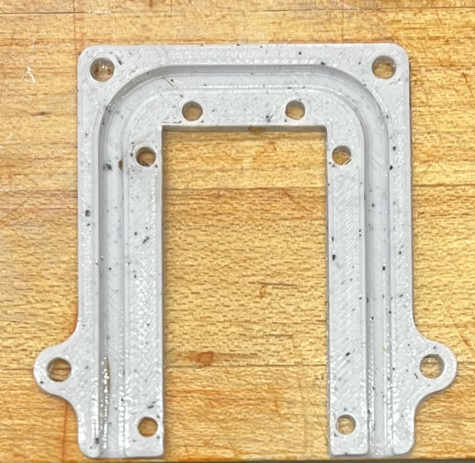
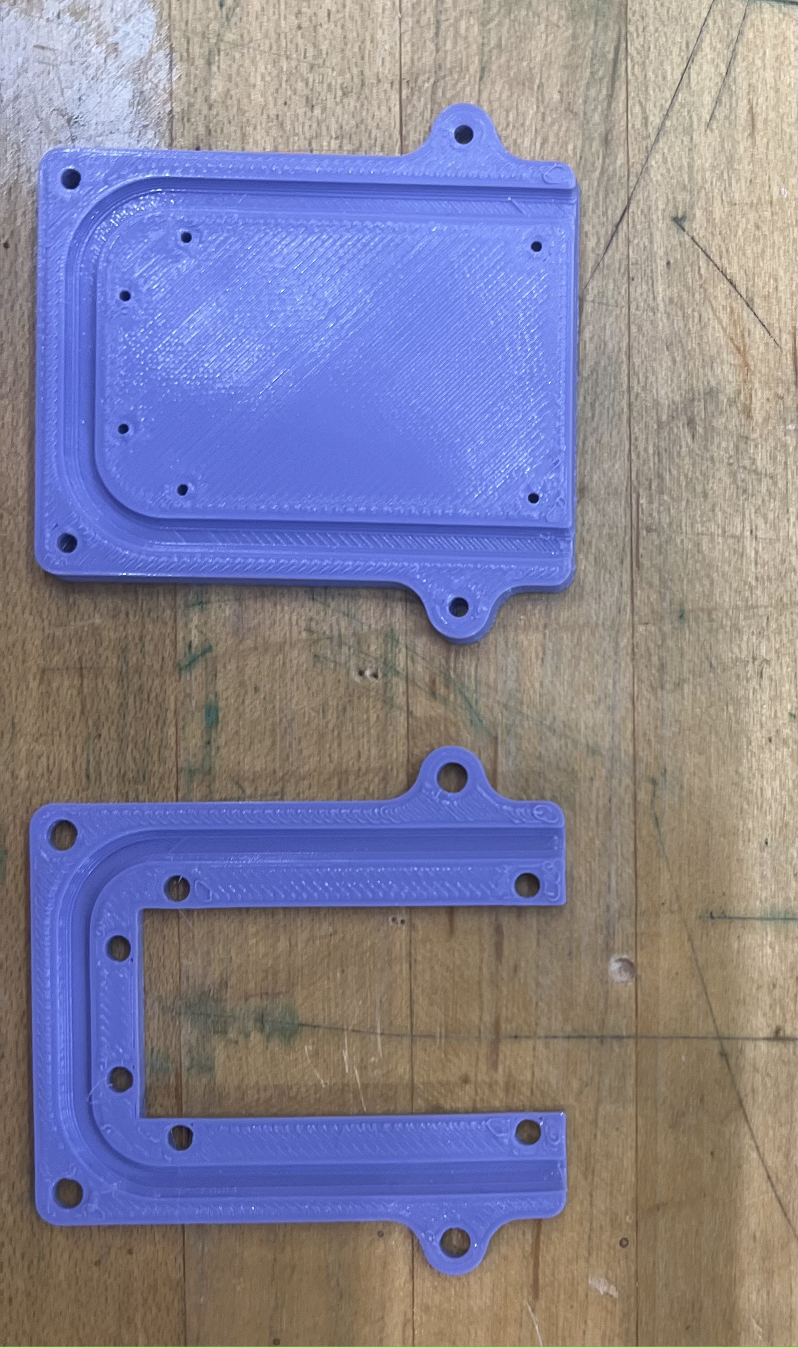
For the filter, I aimed to target a device that could capture and detect PFAS concentration. This encourages rapid PFAS detection for at-home kit applications but also encourages the concentration of PFAS. With reference to the 55cm diameter of the PANI filter paper, I designed my smart sensor filter on Fusion 360. Particular components that I considered during my design included the collection of the analyte solution after filtration (requires collection cup), accessibility of the OLED screen display for the user, incorporation of the copper electrode into the filter, and protection of the PCB board that is incorporated into the device. It was imperative for me to employ parameterization during my design to encourage facile tuning of the product dimensions with respect to the components. For me, I found it difficult to encapsulate each dimension of the PCB board, and account for chord connections, filter paper diameter, and chord diameter to yield an exact print. For this reason, I underwent two 3D prints in order to yield a promising model.
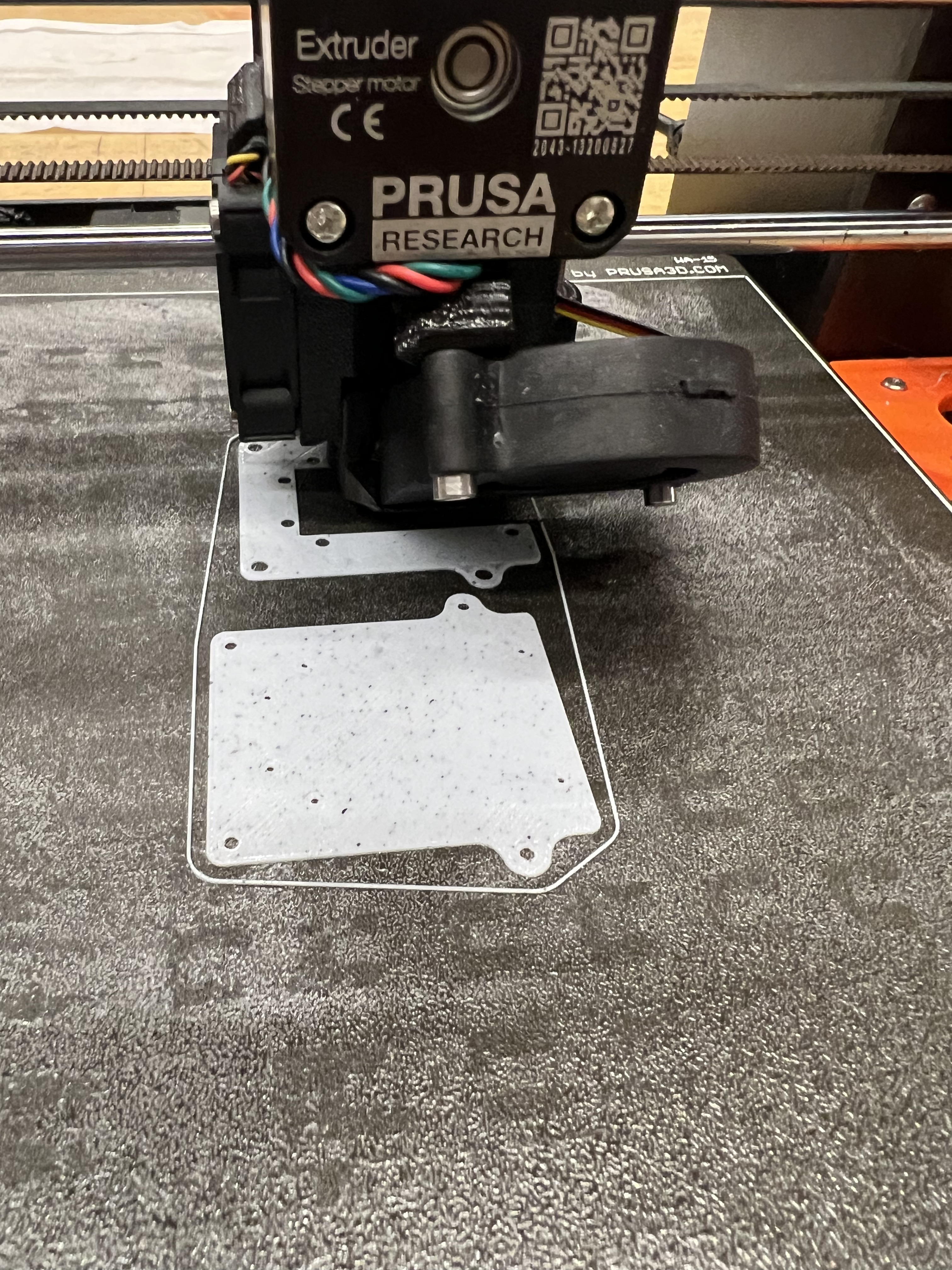
It is also important to consider the material for 3D printing in the case of sensing. As the behavior of PFAS in aqueous media is quite unknown, they have been shown to react with varying polymeric materials. For this reason, I originally targeted polypropylene filament for the Prusa 3D Slicer. As polypropylene exhibits low adhesion to the support bed of the 3D printer, higher heating bed temperatures are needed alongside a nozzle temperature of approximately 220 degrees Celsius. When programming the 3D printer to exhibit these features, unfortunately, this led to the mysterious breakage of 2 Prusa printers. Thank you to Alfonso for your support in troubleshooting these conditions. I hope to eventually print the filter with polypropylene filament in the future. To be continued…
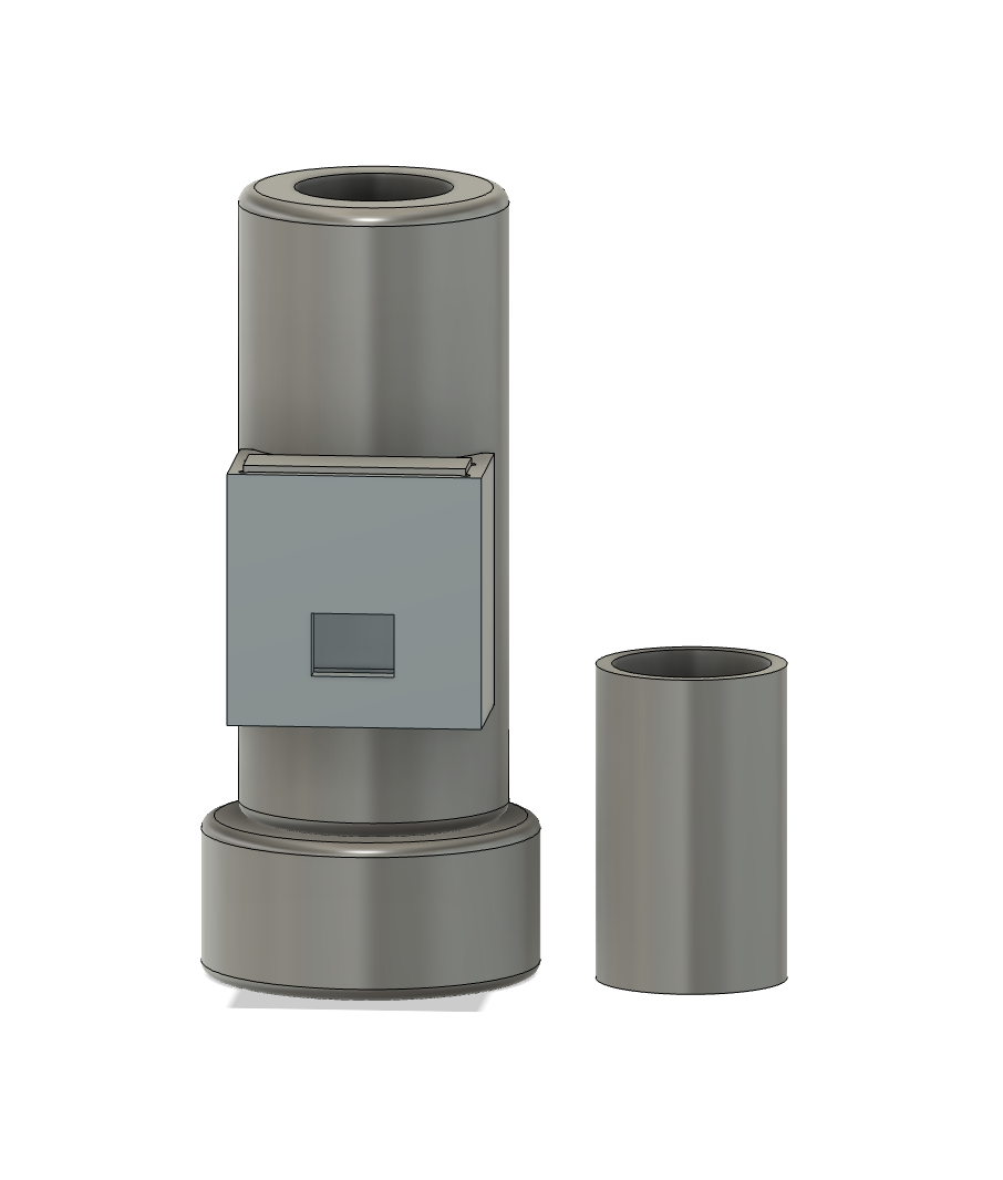
In the case of supports for the 3D prints, these are also quite necessary to consider. In order to yield a well-supported 3D print, I found the organic, tree-like supports to be the best. Particularly, they were easier to remove from the filter, and also provided robust support, especially to the component of the filter, where the PCB board is held. One thing that I did not consider after two iterations of 15-hour prints was that the OLED screen would require an offset for the OLED screen.
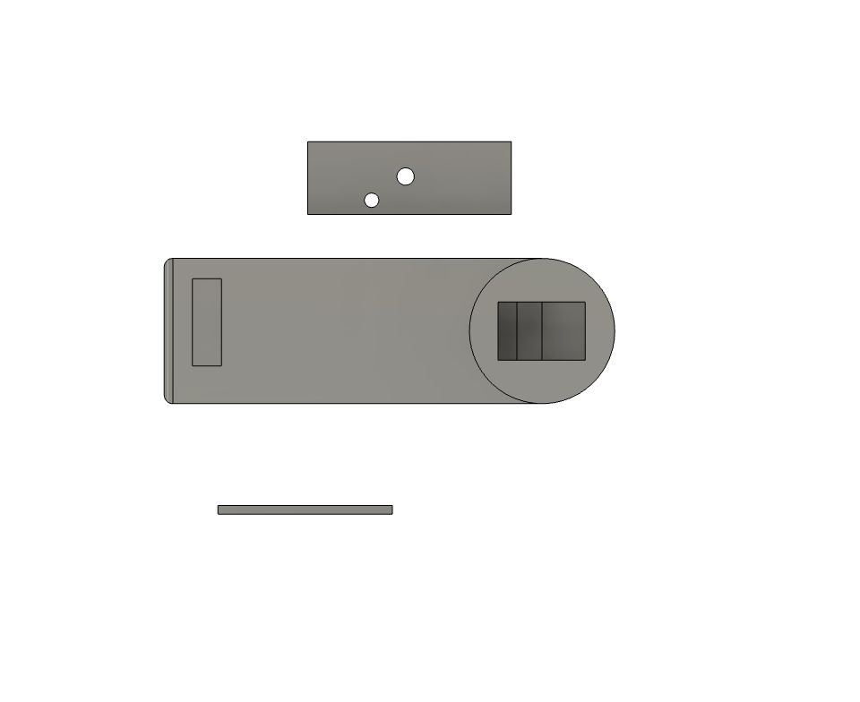
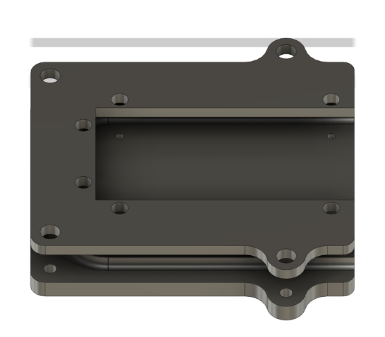
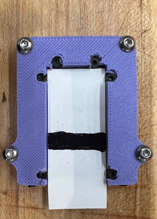
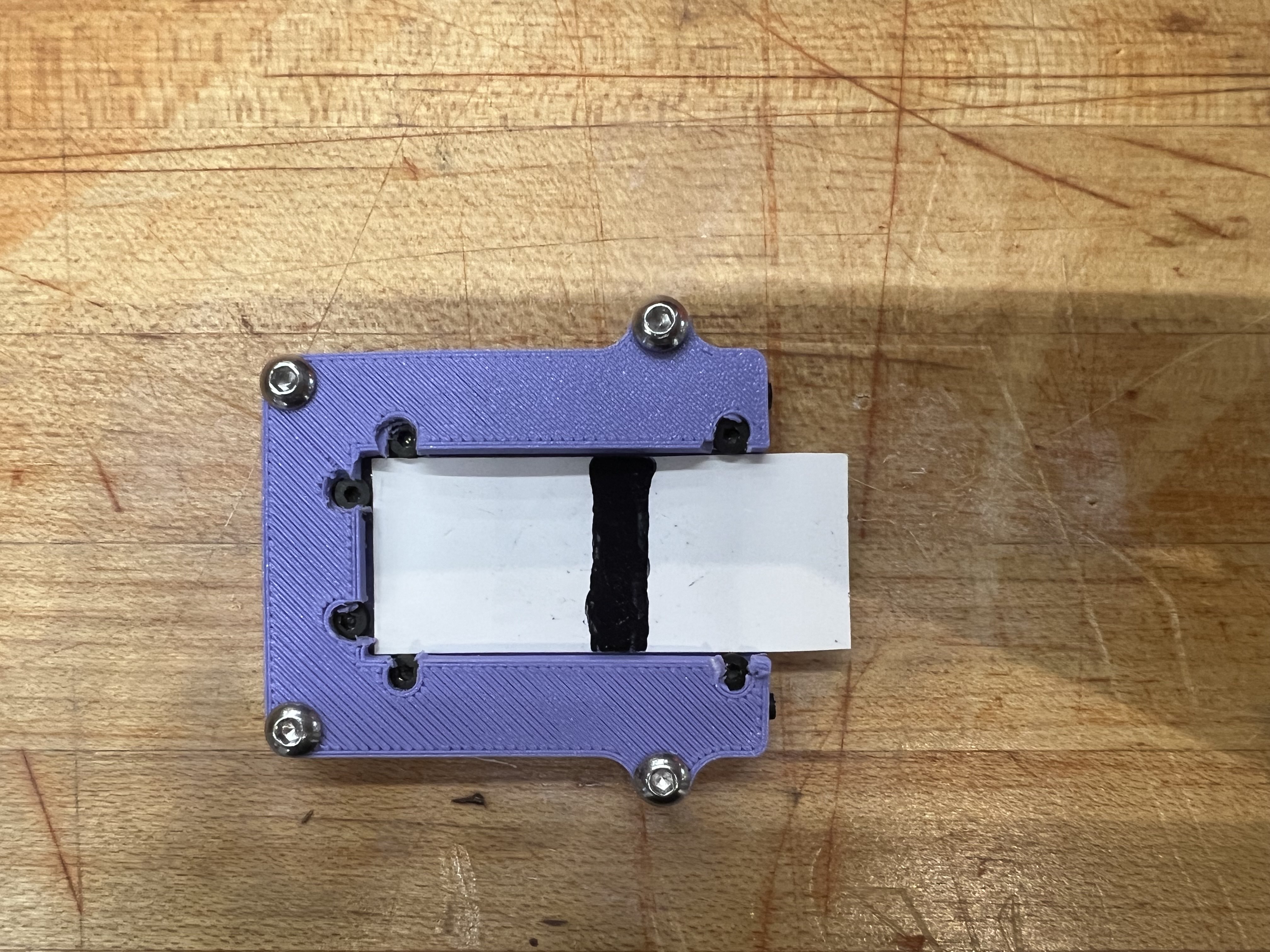
Smart Lateral Flow Assay
The first iteration of the LFA cartridge was embarked on during the fourth week of HTMAA. While this novel LFA cartridge design encouraged a simple flow of the analysis across the polymer membrane, further iterations needed to be explored in order to encourage a user-friendly device that allows for the incorporation of the electronics component for PFAS concentration detection. Another main feature of the smart sensor is that it encourages a reusable device by which the nitrocellulose membranes can be replaced for facile and cost-effective usage. For the LFA, I targeted a sample addition port, where the user can pipette 5 mL of analysis onto the sensor membrane. From here, upon 30-minute incubation time, an accurate PFOA concentration readout can be acquired with respect to previous sensing studies in the Swager Lab.
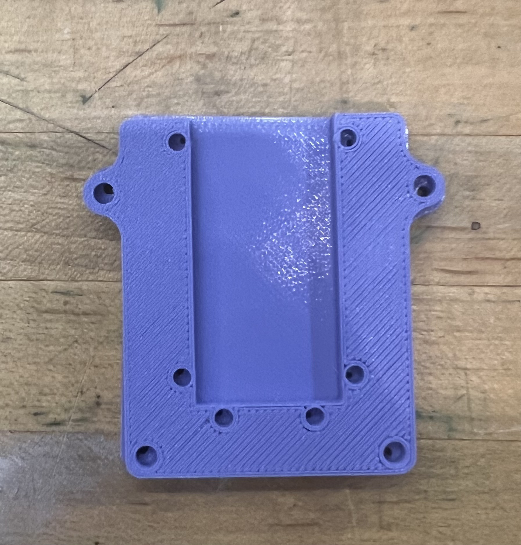
The smart LFA cartridge was designed in Fusion 360, with reference to the size of the PCB and its components, alongside the SSD 1306 OLED display, and the nitrocellulose membrane (50mm x 60 mm). In addition, I had to account for the incorporation of the copper electrodes on both sides of the polymer coating to monitor the resistance over time. It is also important to account for the incorporation of the wiring within the device in order to allow for connection to the USB-C of the ESP-32C3 on the PCB board alongside encouraging the LFA to be waterproof.
This design was also printed with a Prusa-3D Slicer, with a print time of 6 hours on PLA filament. It is important to note that two iterations of the design were targeted due to support issues in this case. The first design unfortunately experienced a high dip in the LFA loading port, due to a lack of support. In response to this, I increased the thickness of LFA and employed organic supports. In comparison to the filter, the organic supports were quite difficult to remove and did not prove to be as hollow.
Assembly
In assembling my sensing devices, I did not aim to employ any screws. I particularly targeted “snap to fit” connections. Particularly, I targeted cartridges that encapsulated my PCB board with room for USB-C and electrode chord connections. The assembly was most definitely a demanding process as it required two iterations of 3D prints to account for the chord size alongside the PCB board size. I did reinforce the importance of parameterization here, alongside the mantra that “it takes multiple prototypes to yield a promising product.”
Sensing Studies
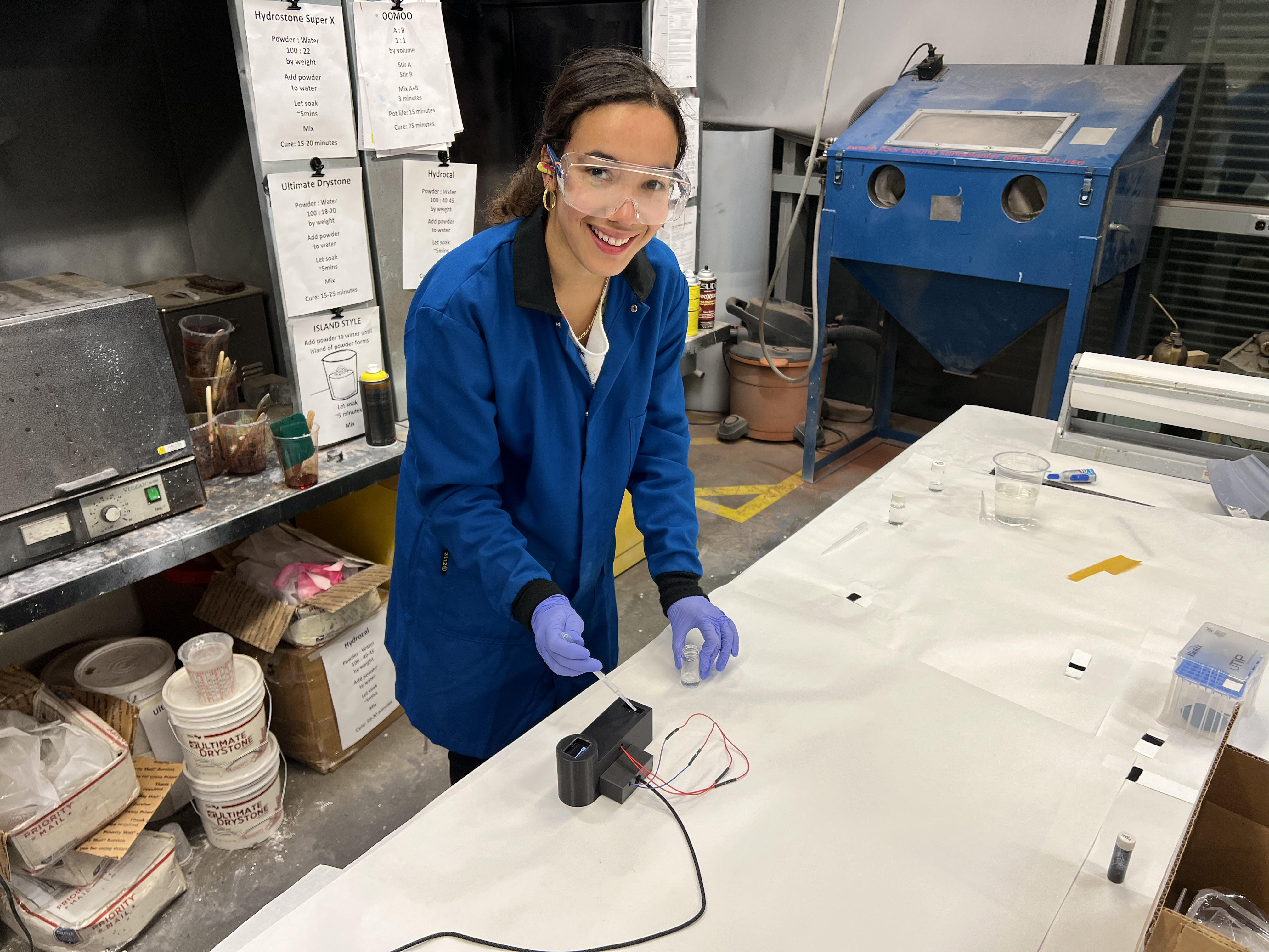
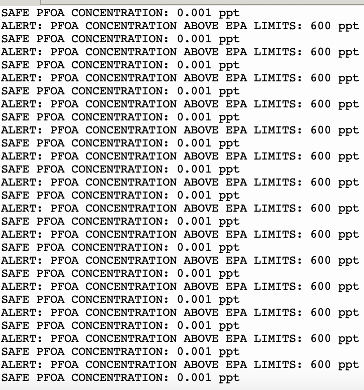
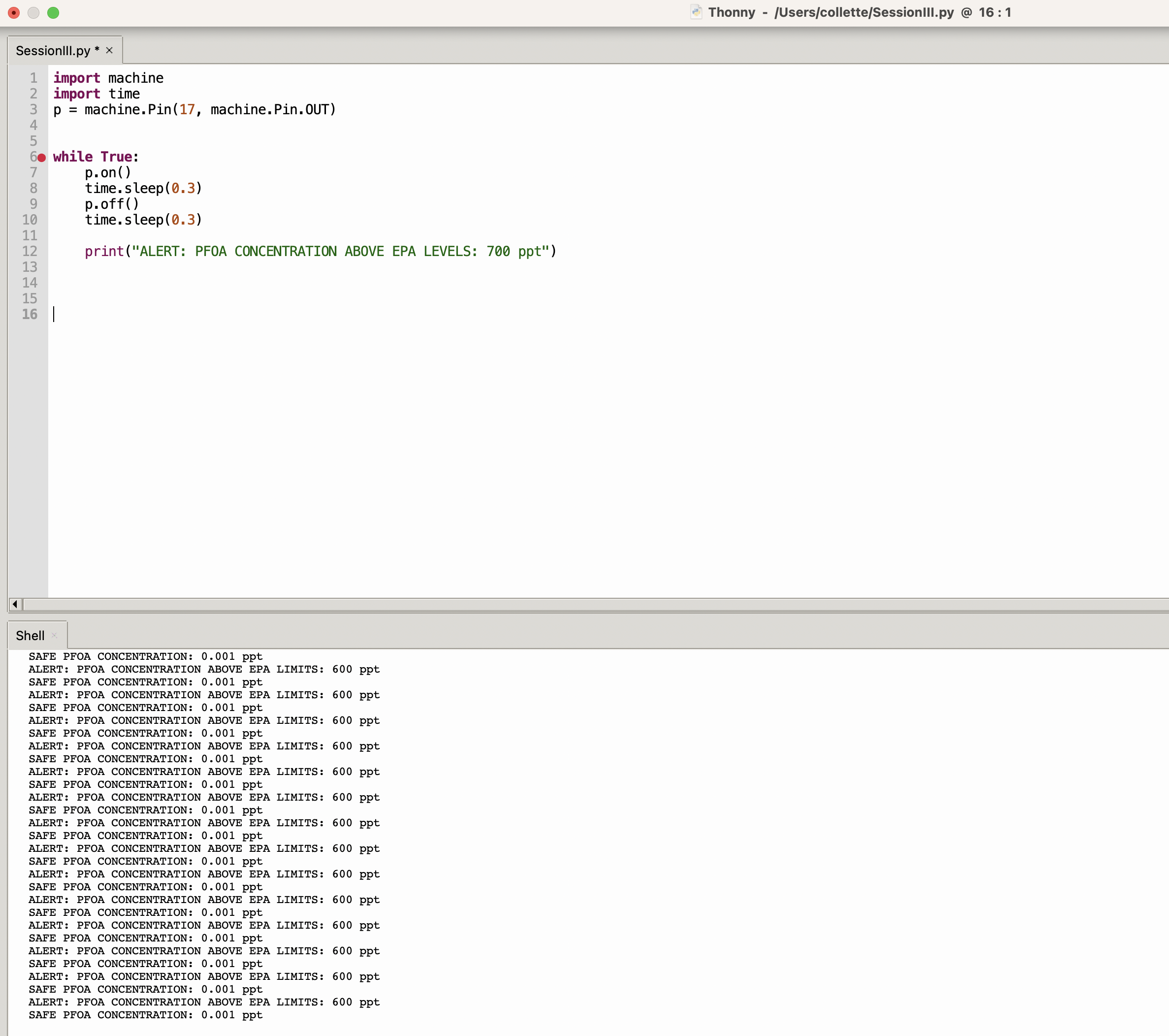
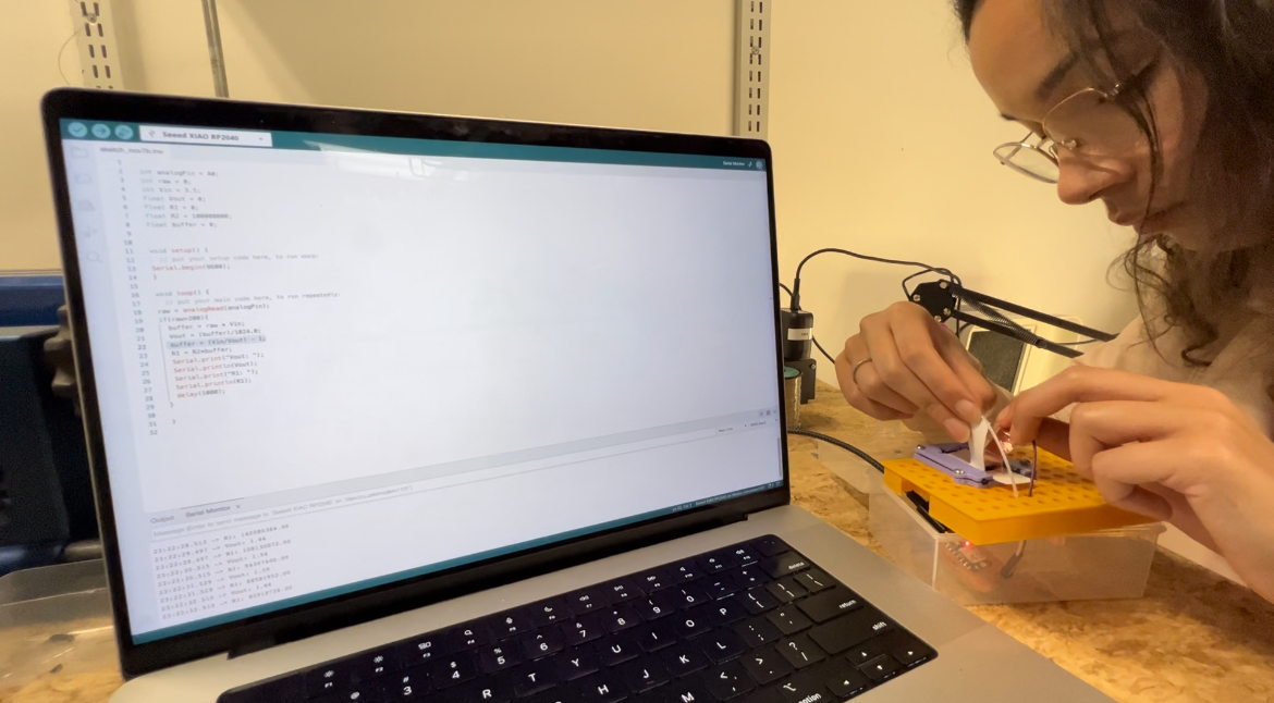
With an interest in monitoring the concentration of PFAS in solution, I carried out sensing studies of water from the CBA shop, which interestingly is an unclear solution. For the LFA, I pipetted 5 mL of aqueous analysis to fill the well followed by 5 minute wait time to encourage the absorption of the analyte by the polymer film. For the filter sensing studies, a similar pathway was followed, aside from the increase in the volume of analyte analyzed (in this case, I measured the resistance of 50 mL of water). For resistance measurements, I monitored the resistance following calculations with a voltage divider and then converted it to the concentration of PFAS (with reference to previous studies on the relationship between resistance and PFAS concentration studied in the Swager lab).
I observed that there was an average of 600 ppt PFOA concentration in the CBA shop water, which is above the EPA LOD (4 ppt). Further time-point studies must be employed in order to determine the optimal time to measure the resistance of the polymer film in order to yield the most accurate readout.
Making Over Buying
Throughout my final project, I aimed to create my 3D designs and electronic devices with the incorporation of an XIAO-ESP32-C3 Microcontroller without purchasing many components. I polymerized the PANI films in situ on cellulosic membranes via interfacial polymerization. For the PANI-ink preparation, I employed the interfacial polymerization of PANI followed by dispersion in water to form stable ink solutions.
3D Designs: While the intended material for the cartridge and filter was polypropylene(PP), due to a series of unfortunate printing concerns, I ended up employing poly(L-lactide) (PLA) filament for ease of printing. While certain components of the filter and cartridges could have been purchased and assembled, I designed each of my sensor cartridges on Fusion 360 and printed them with a Prusa-3D Slicer.
Electronics: While I did employ the commercial SMD 1306 OLED display alongside the commercial ESP32-C3, the PCB board trace design was created by me alongside the functional goals. I did not utilize a breadboard during the electronics portion, but I did make good use of the multimeter in order to analyze the connections within my circuit.
Future Work and Aspirations
In the future, I aim to optimize the resistivity sensing by incorporating a copper electrode with increased contact with the conductive polymer paper. In addition, I aim to further enhance the smart sensor designs by targeting less visible connection cords alongside a polypropylene print. Overall, I hope to eventually expand the smart sensors for commercial applications in order to encourage the public to develop a stronger understanding of the composition of their water. In reflection, I am very grateful for the opportunity to take the HTMAA Course. I have learned a myriad of life-long skills about how to cultivate and create products of my interest with tools acquired in 3D design, electronics, assembly, and signal processing. Thank you to Neil, for being an amazing Professor.
I would like to give a huge thank you to Alfonso for supporting me throughout my final project development, I am very grateful. Thank you to Quentin and Anthony for your kind guidance!
Design and Inspiration
PFAS, known as per(poly)-fluoroalkyl substances, commonly referred to as “forever chemicals”
present major health risks to humans and the environment. With a rise in environmental
health concerns, there is a major demand for sensors to selectively detect environmental
markers.
With the intrinsic goal of detection of PFAS, I aimed to target rapid, selective PFAS
detection through the use of Lateral Flow Assays and Filters. My goal for extending my
original focus to filters was to target the capture and detection of PFAS, which can present
a possible solution for PFAS removal from water supplies at homes and industries.
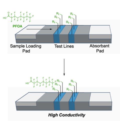
While point-of-care diagnostic (POC) treatment employs lateral flow assays
for the colorimetric and fluorometric sensing of biological and environmental analytes, few
studies have employed conductive polymers for the quantitative sensing of environmental
analytes. This final project aims to employ a series of conductive polymers fabricated onto
a sensing device for the quantitative detection of environmental markers. As the conductive
polymers exhibit an extended pi-conjugated backbone, facile reduction, and oxidation upon
introduction to the analyte will encourage selective limits of detection. Through employing
the Fusion360 Software, the sensor prototype will be modeled, built, and enhanced throughout
the course of this semester.
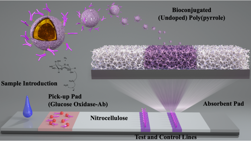
The e-LFA will contain a sample loading and absorbent
pad, that through capillary action drives the fluid through the nitrocellulose membrane to
deliver the PFAS to the F-PANi fabricated test lines, which are proposed to induce an
increase in conductivity upon introduction to PFAS. In the polymer synthesis lense, the
selectivity of a library of functionalized F-PANi polymers for e-LFA will be fabricated onto
the sensor.
For my final project, the overall goal is to design am electronic-conductive polymer
fabricated sensing device that can quantify PFAS Concentration in water with reference to
the EPA limits of detection of 4 ppt. My main three goals for the final project include:
1. Selectivity for PFAS of all chain lengths over non-fluorous compounds
Synthetically, the fluorophilic and hydrophobic effect will be targeted to yield covalent
and ionic perfluoroalkyl moieties incorporated into the polymer network for selective PFAS
detection.
2. Reusable and Cost-Effective Device
The cartridges for the sensor will be targetted through laser-cutting PMMA poly(methyl
methacrylate).
3. Rapid and Wireless Readout of PFAS Concentration
Copper Electrodes with 20-30 resistors will be fabricated onto the PMMA cartridge to measure
the average conductivity of the polymeric films. From here, the conductivity can be
extrapolated with reference to the bulk resistivity of the film.
Conductivity = σ = 1/(bulk resistivity*film thickness)
- Wireless signal will be employed by incorporating the ESP 32-C3 microcontroller into the
electronics board design. From here, with Arduino IDE C++ Code, the wireless readout of the
conductivity can be programmed and communicated with devices.
- Output screen on the sensor cartridge will display the PFAS Concentration in the Water and
indicate whether the PFAS Concentration is above the EPA Limits of Detection.
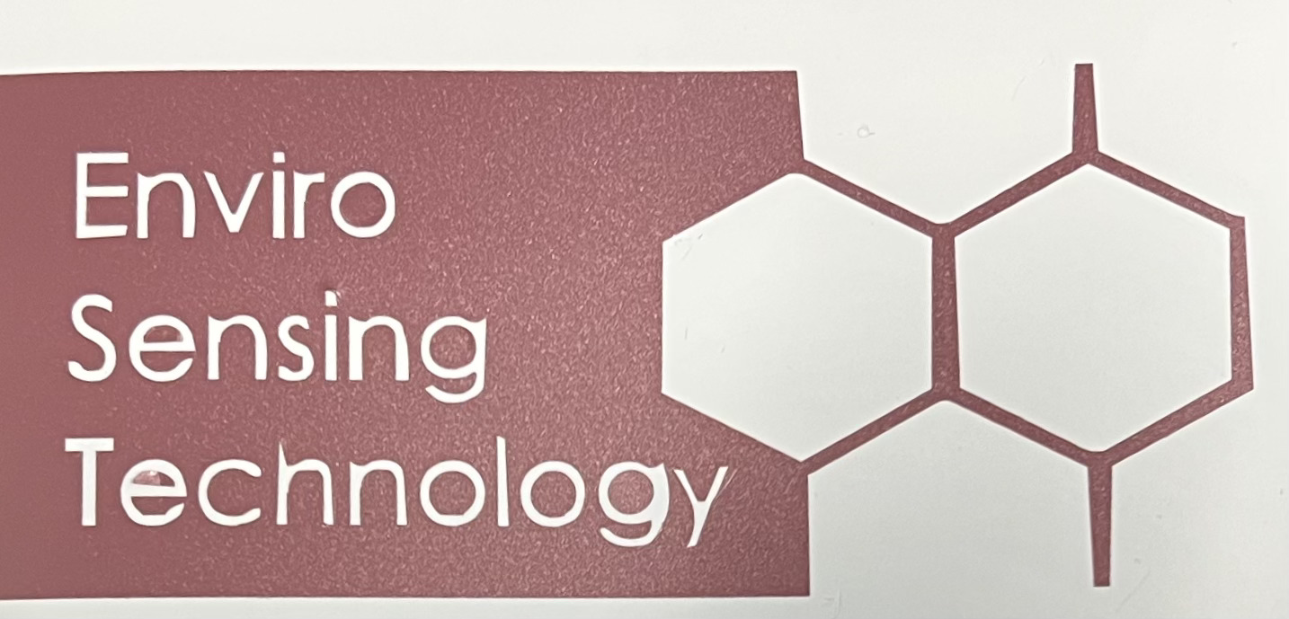
With an interest in creating a label for my sensor, I decided to target "Enviro Sensing Technology." In order to design my label, I employed Inkscape Software. Particular commands of interest and assistance included Object-Mask-SetInverseMask in order to cut the designs.
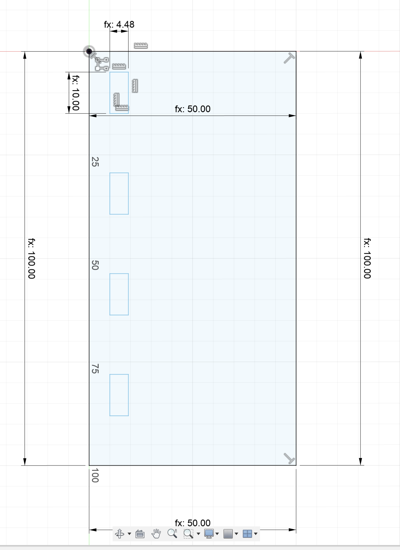
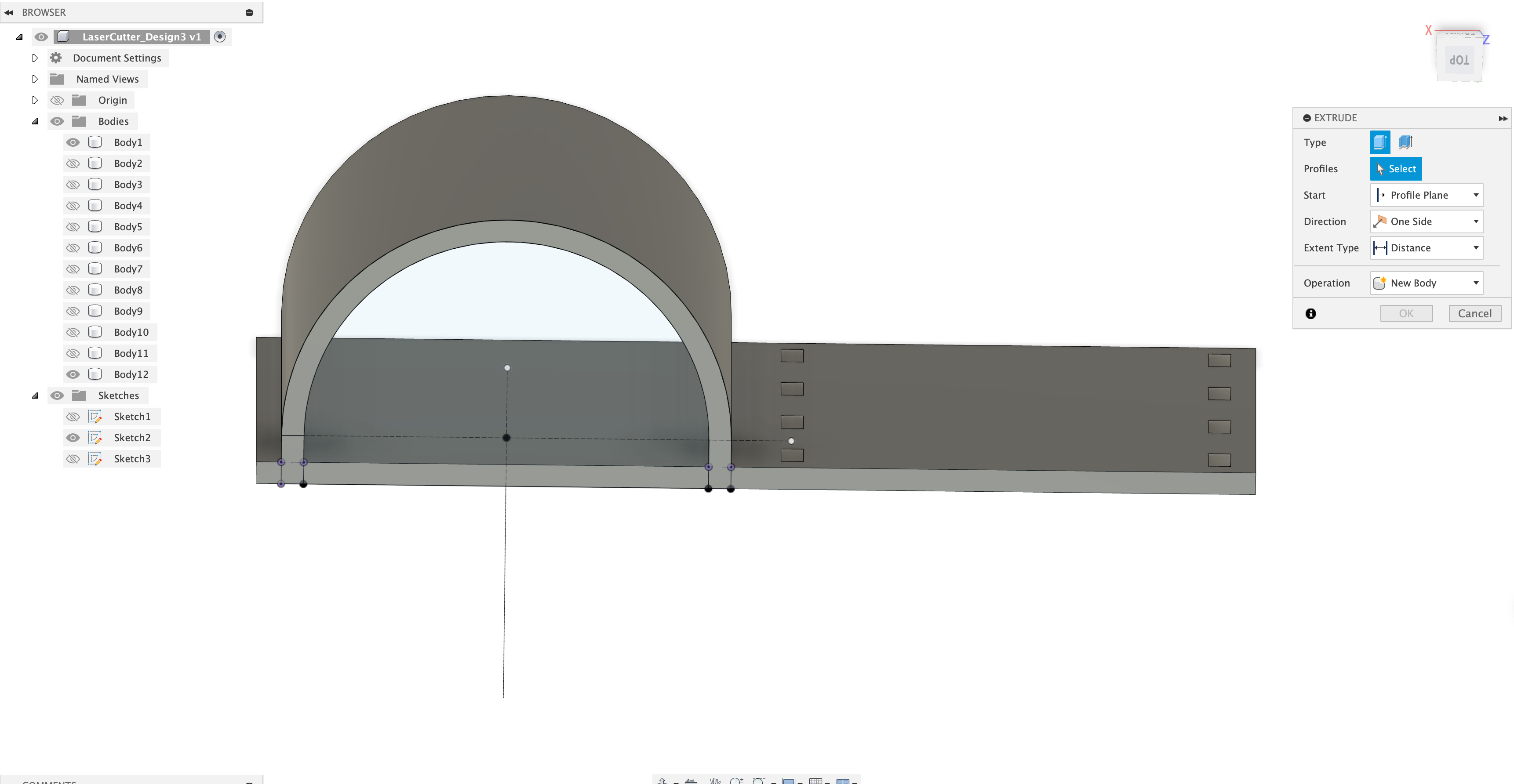
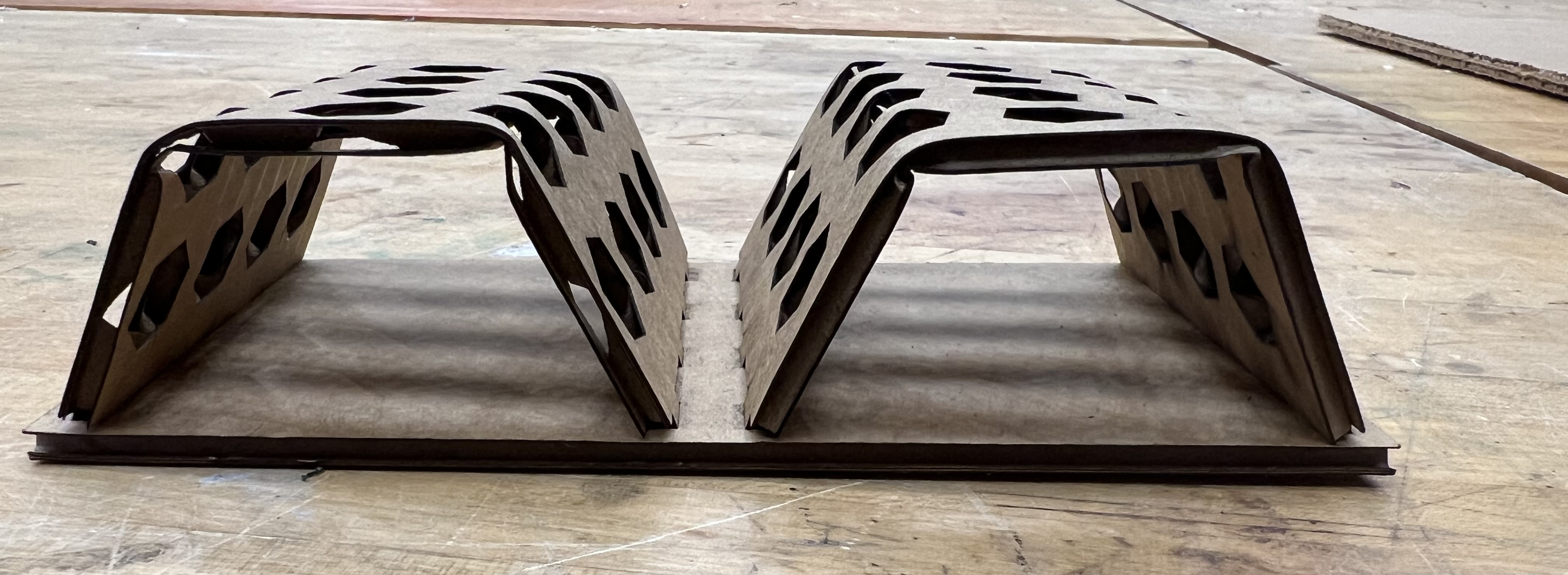
Learning to employ Fusion360 for 3D design was a fun and challenging
endeavor. With an interest in designing a bridge platform with two arches, I first sketched
the base of the bridge. After measuring a thickness of 4.48 mm with the caliper, I went on
to begin my drawing. Through this journey, I learned the l feature in order to begin my
sketch along with the importance of parameterizing each feature and the mirror image feature
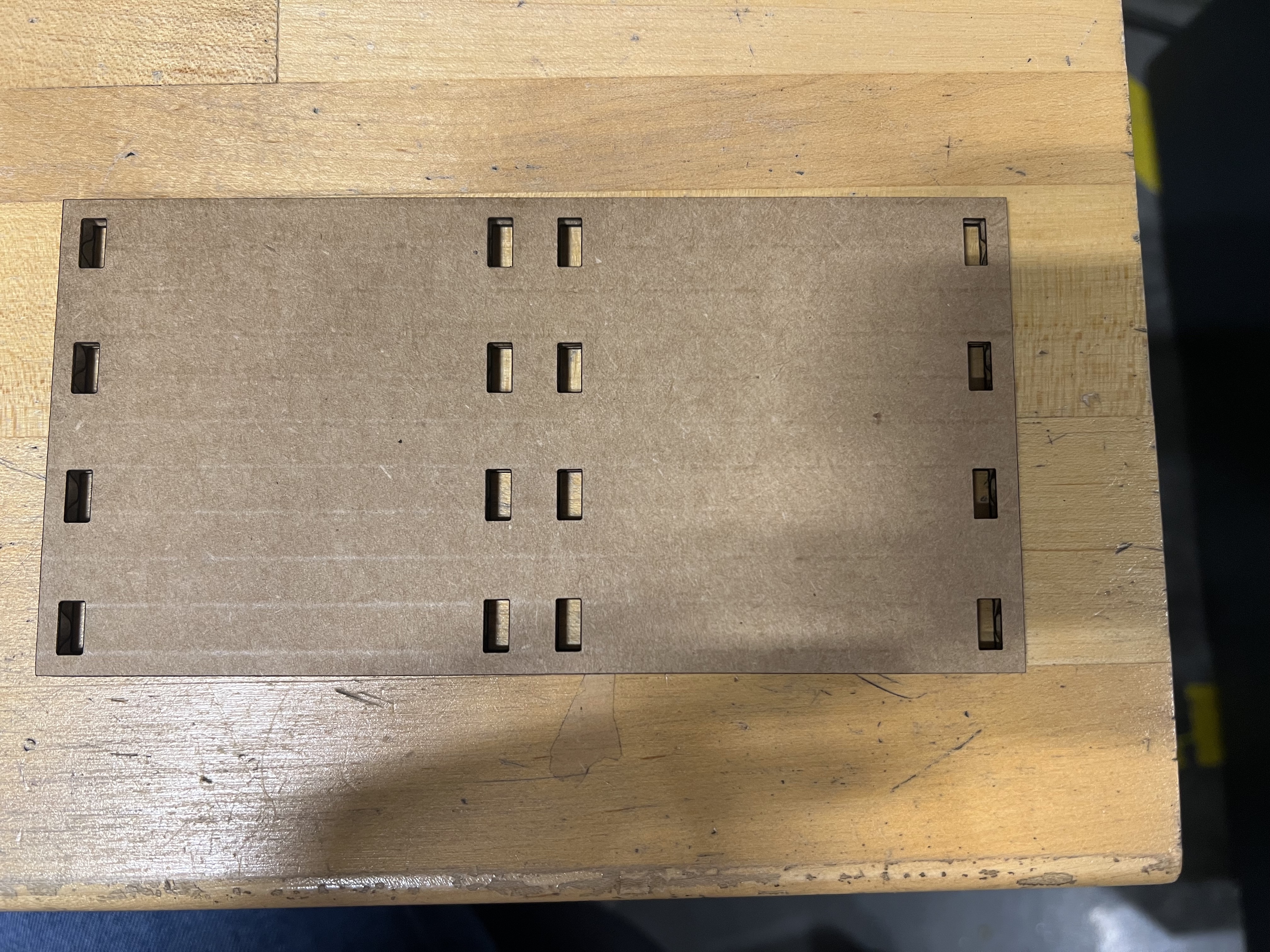
for future replication. The base of the arch included rectangular slits for assembly, which
were achieved through the rectangular pattern with a slit width of 10 mm and thickness of
4.48 mm. The split cell feature was also employed to create a new document.
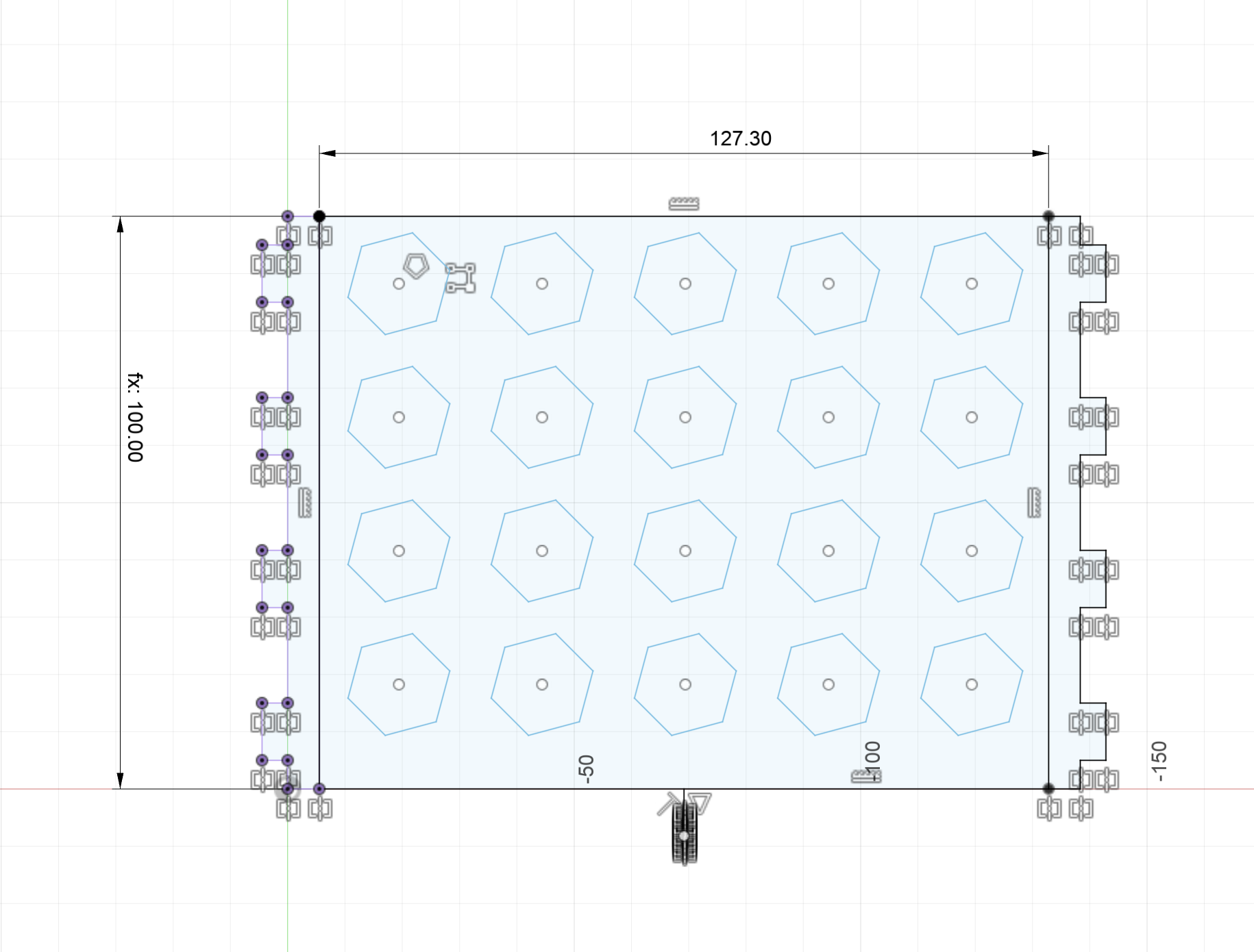
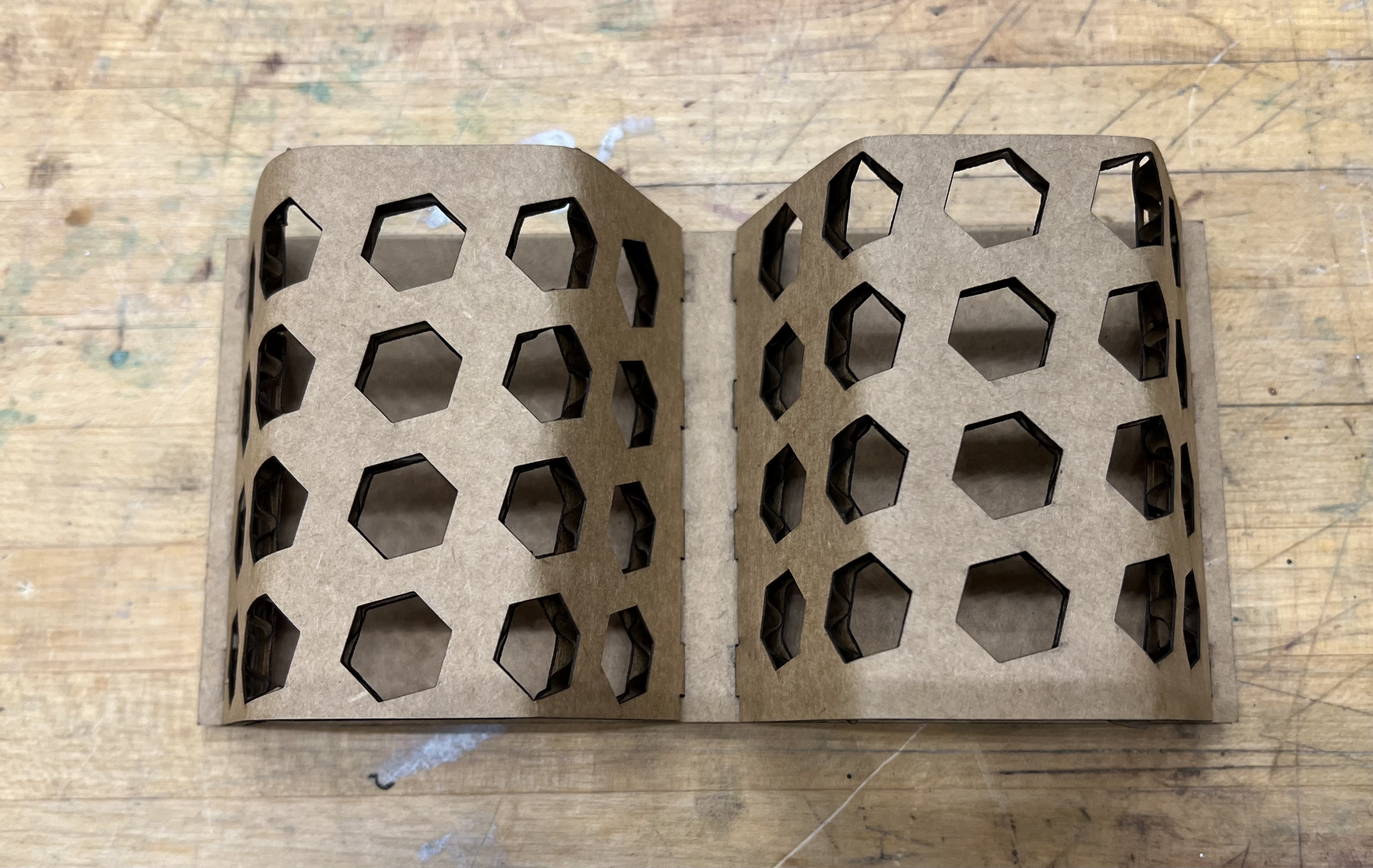
In order
to encourage arch flexibility with a cardboard material, I chose to extrude the cyclohexane
rings onto the arch plane. The kerf chosen was 0.2540 mm, and the dimensions of the base
were 100 mm x 50 mm.
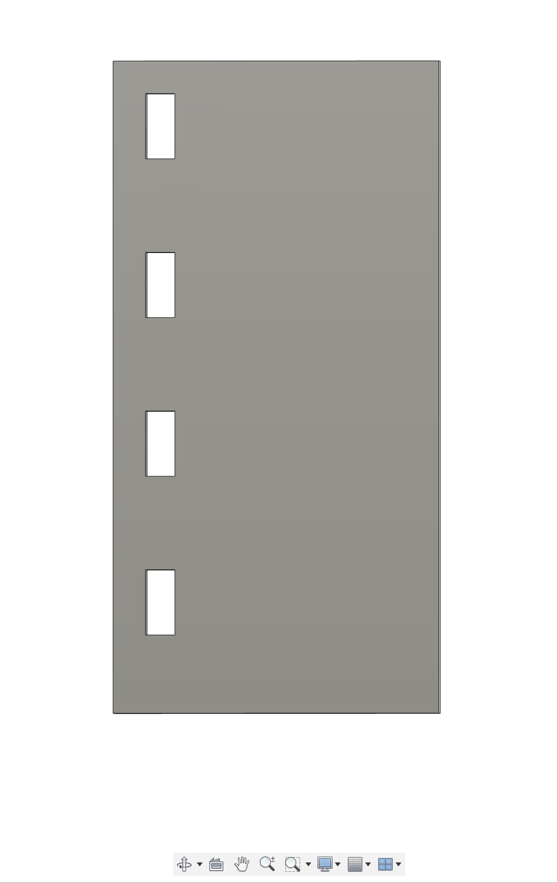
Upon yielding Fusion Sketches of the base and arch, both
sketches were saved as DXF files. Interestingly, the printer did not accept the DXF files,
so an SVG file was employed instead.

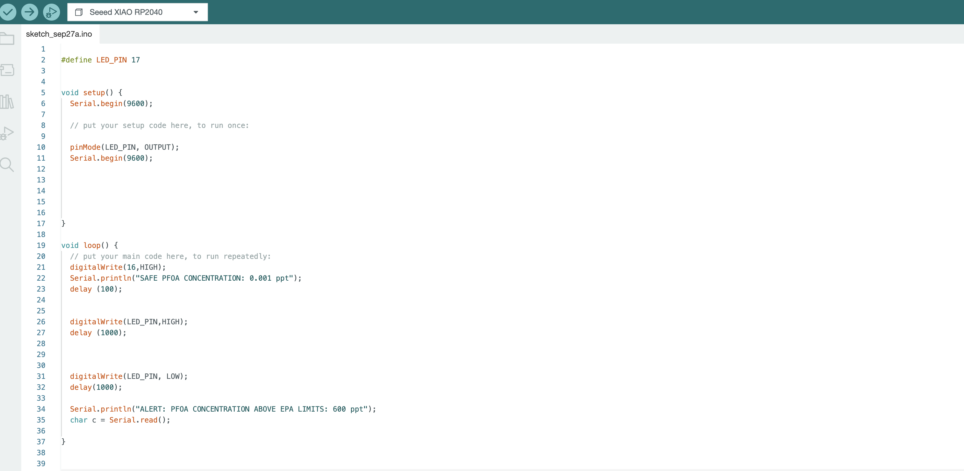
This week, I focused on employing Arduino IDE and PythonScript for the prgramming of a seeed Studio Xiao RP 2040 circuit board. With an interest in the wireless readout of PFA concentration for my final project, the goal of this week was to develop program that reports flashes red (indicating PFOA concentration above EPA limits), and a program that flashes green (indicating PFOA concentrations below EPA limits). The Xiao RP2030 has 32 GPIL ports, by which only 14 are accessible. With respect to the the schematic for the RFP, one can note the LED light locations: Blue: GPL25 Green: GPL 16 Red: GPL 17 To factory reset the circuit board, press: R = rest, runs code from scratch B = factory reset mode In Arduino, a part of the system employed a bootloader to convert the Arduino code onto Micropython from the circuit to the server. Thus the Arduino code was running on Python and alerts were reported.
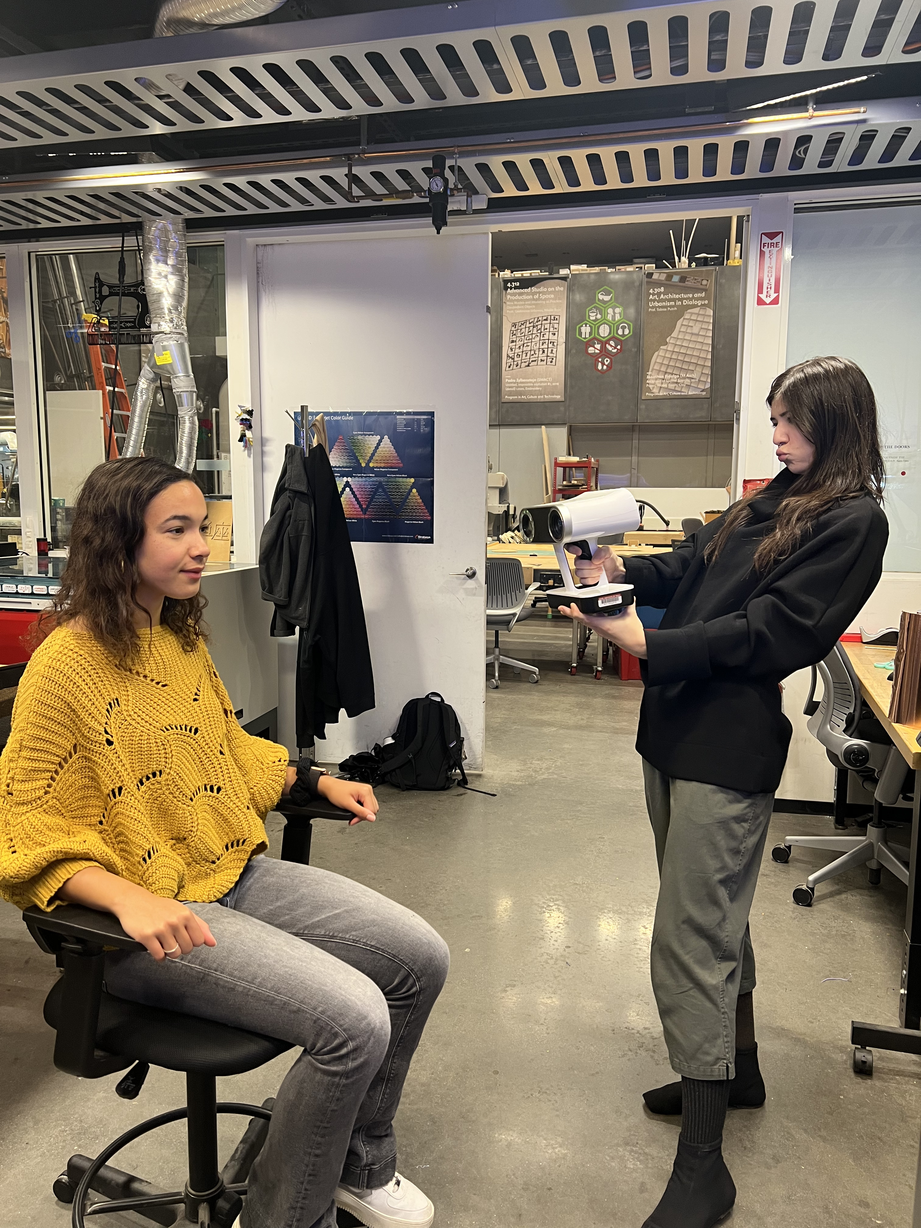
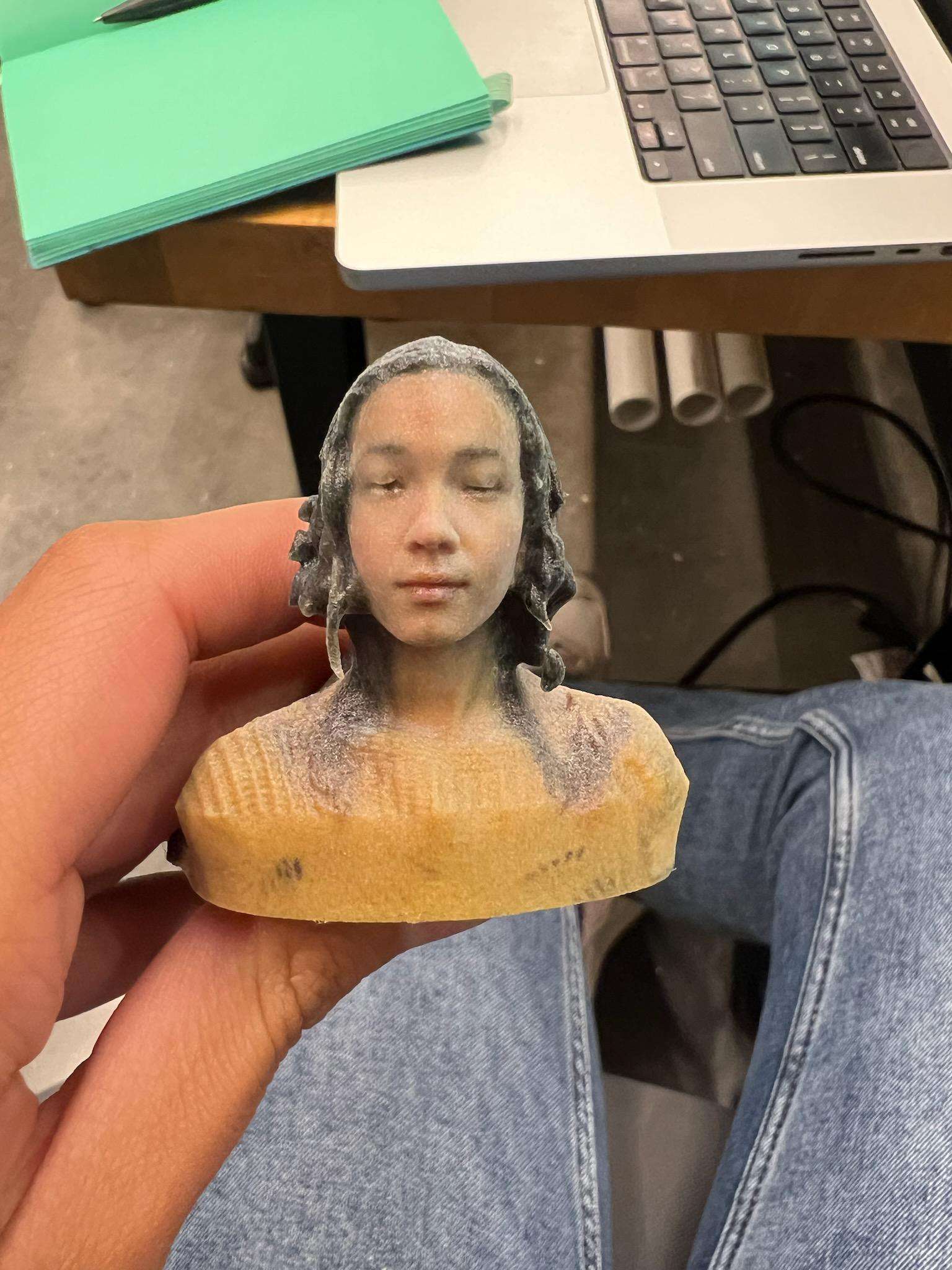
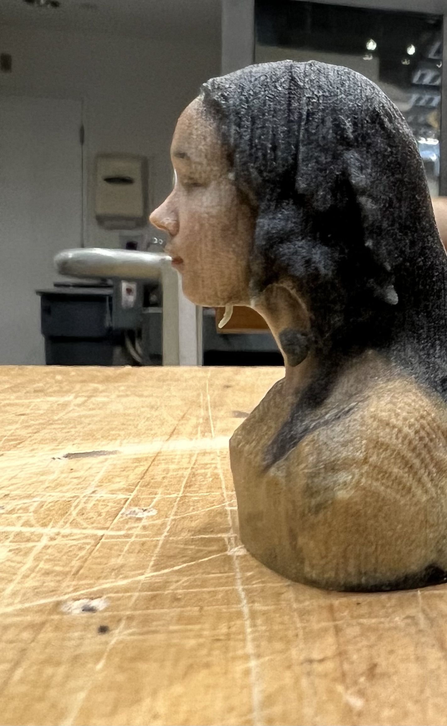
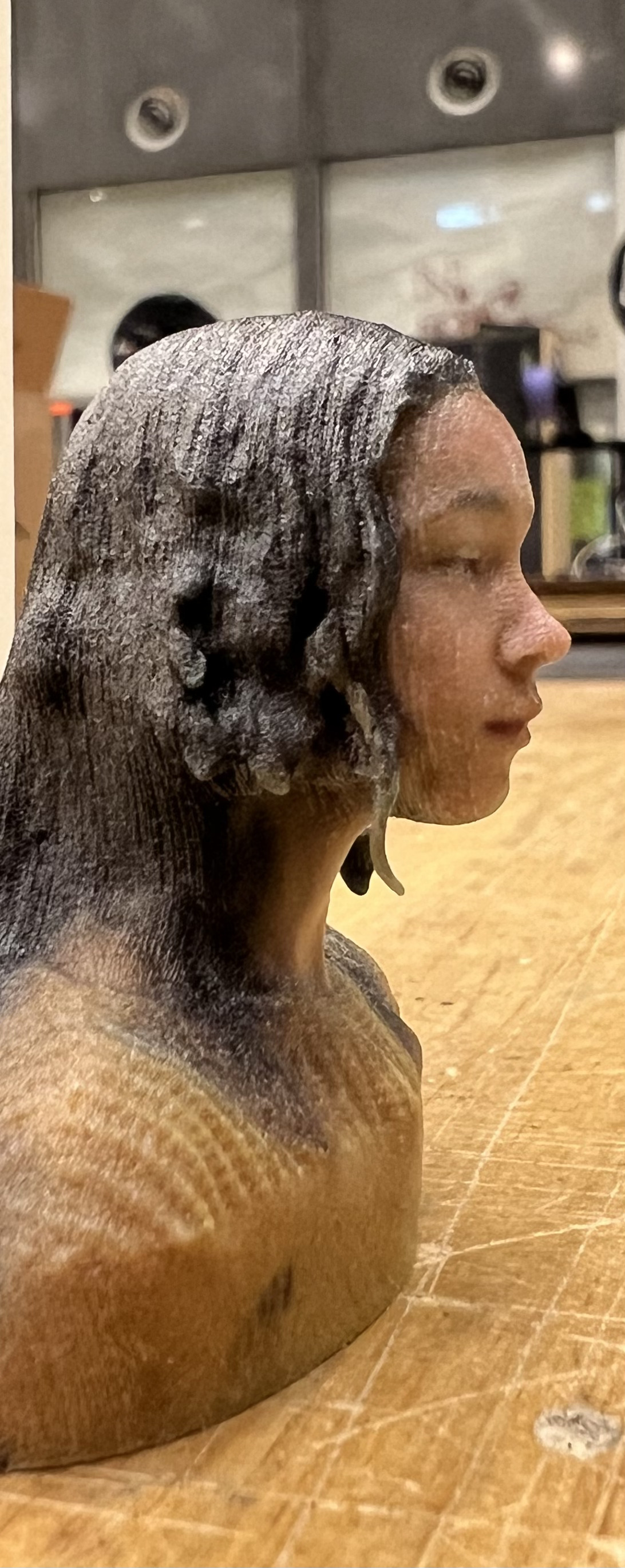
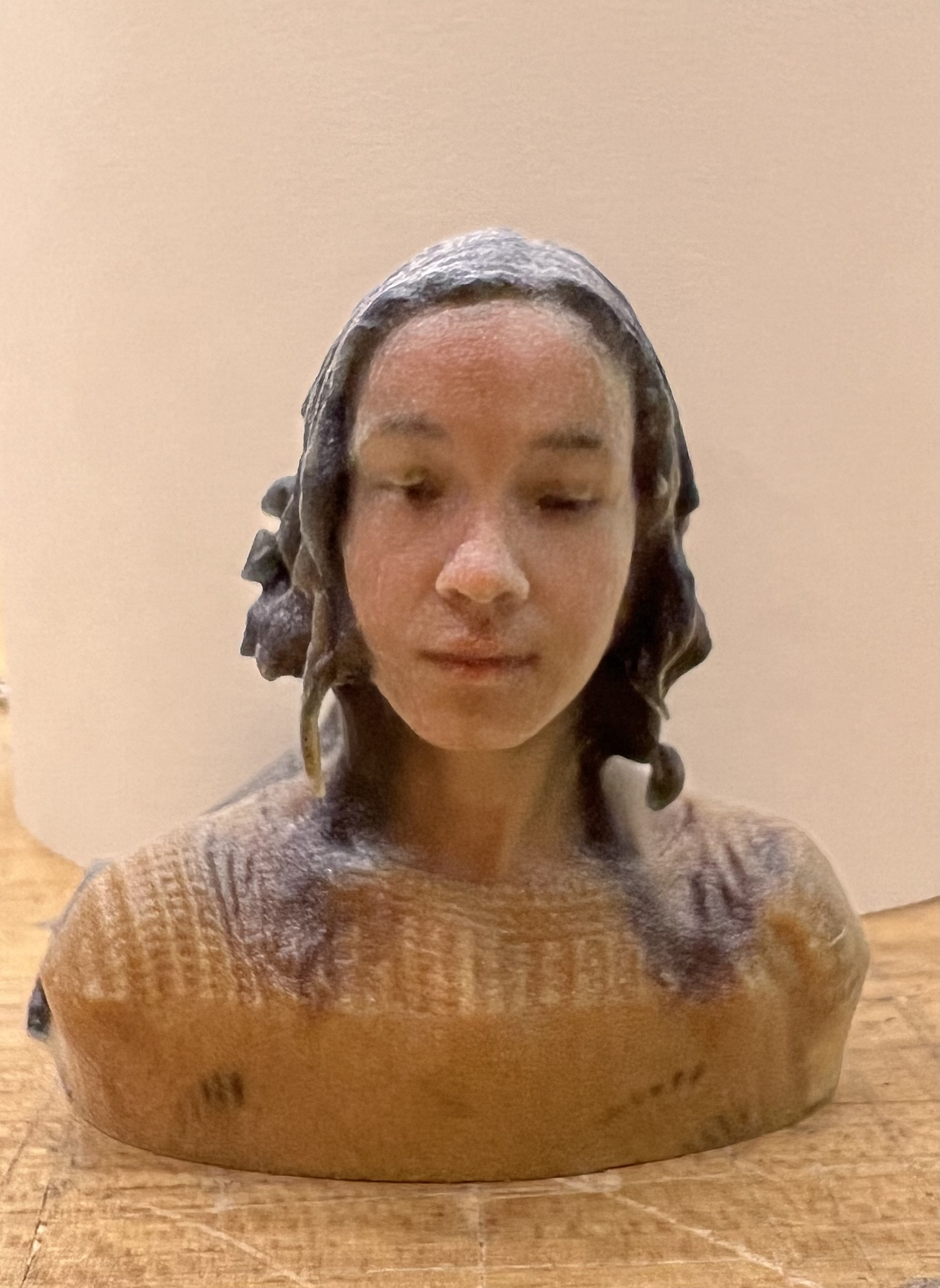
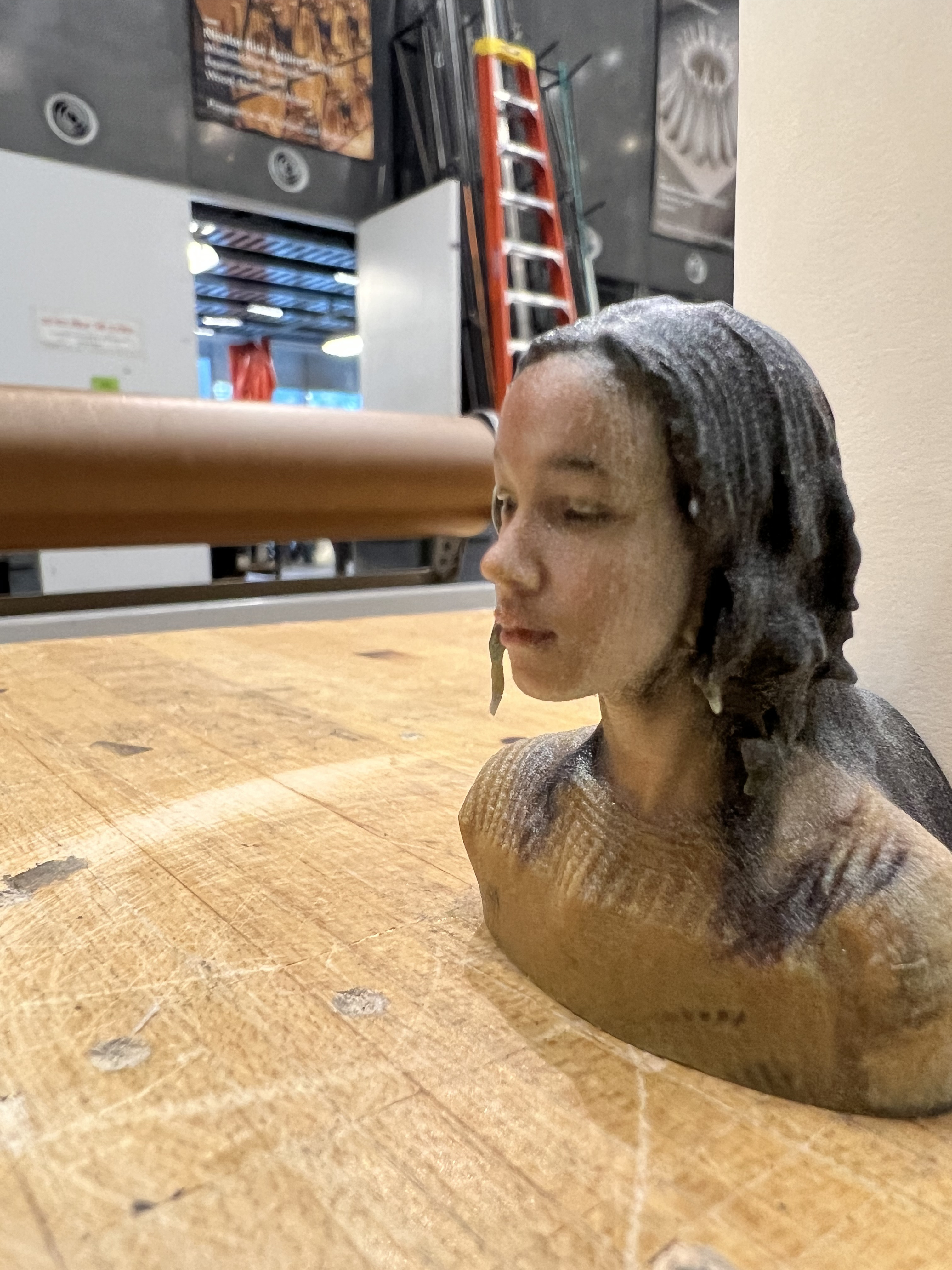
For this week’s 3D scanning design, I was excited to carry out self-portrait scans with Char and Gayuri. We employed the Artec LEO 3D Laser Scanner in the CBA shop and scans were tuned with the Artec LEO software for further tuning of designs through tuning the mesh and scaling. Creality was utilized to prepare the STL files for 3D printing. Unfortunately, the first scan inaccurately accounted for my eyes and facial structure. Thankfully, Char and Gayuri took another scan of me, which looked more representative! I will admit my curls were not fully captured, but I am excited for more scanning in store!
In an effort to target a cartridge prototype for the quantitative detection
of environmental analytes, I targeted a Lateral Flow Assay Cartridge this week. During my
designing phase, I employed Autodesk Fusion 360 Software. Features of Autodesk Fusion 360
that I found quite useful included the parametric design of the diameters of the circular
holes and dimensions of the test strip and the base cartridge.
Lateral Flow Assay
nitrocellulose test strip
D1 = 20 mm
D2 = 40 mm
The base cartridge has
dimensions of 40mm x 60 mm.
The sweep feature was helpful in order to secure the
lateral flow assay with a Teflon ring. The dimensions of the curve:
CL1= 46 mm
Cl2 =
32 mm
Arc = 8 mm
The mirror feature allows for symmetry of the sketch and was
quite useful when drawing the circular holes for the screws with diameters of 1.2 mm and 2.0
mm, respectively. The tangent feature allowed for the constraint of the circles to the
polymer film outline, encouraging the security of the sample in place. In extrusion, the
bottom part of the cartridge was extruded to a thickness of 3 mm, while the top of the
cartridge was extruded to a thickness of 2 mm. In assembly, the M2 and M3 screws will be
utilized to secure the polymer film to the cartridge.
The Fillet feature was employed
to generate curved edges of the cartridge with a dimension of 2 mm. The base cartridge has
dimensions of 40mm x 60 mm.
Thank you to Alfonso for helpful guidance in Fusion
tools!
As the original polymer choice was a recycled PLA, I believe the 3D printer
was heating above the glass transition temperature of the polymers and led to some defects
in the prototype. For this reason, the polymer chosen was a homopolymer of PLA and produced
a structurally-sound prototype to be assembled with M3 and M2 screws.
Despite a quite hectic two weeks with fellowship applications and my first
group meeting, I was eager to begin my circuit board design this week. With complex final
project aims to measure the resistance of a polymer coating over time to measure the
conductivity, my primary goal of this week was to develop a stronger understanding of the
electronics design in Eagle which offered a smooth transition from my use of Fusion 360.
This week my project focus was to incorporate a button and LED light into a Seeed XIAO
RP2040 microcontroller and circuit layout.
Within my electronics design scheme, I
focused on employing a resistor in order to control the flow of current to the button and
the LED light. Furthermore, I also employed a pull up resistor set up for the button with
the grounds connected. Both approaches are preferred as they prevent the buildup of current
and a potential shortage.
As I plan to extend my design for further sensing
applications, I employed a connector with pins in order to encourage further output sensing
in the future.
Notably, the RP 2040 exhibits 2 processor cores with 30
multifunctional general purpose input and output ports, alongside a 4 channel ADS with an
internal temperature sensor.
A few key pieces of terminology that I have learned
include:
GND = external ground
SMD = Surface Modified Device
Key Features to
Eagle Fusion 360, which aided me in my work include:
- Naming connections for clear board
diagrams
-Add feature with access to priorly downloaded fab class circuit components
-Starting
with a simple board layout including an LED light and switch. From here, I made iterative
edits with an increase in complexity with the pin connections.
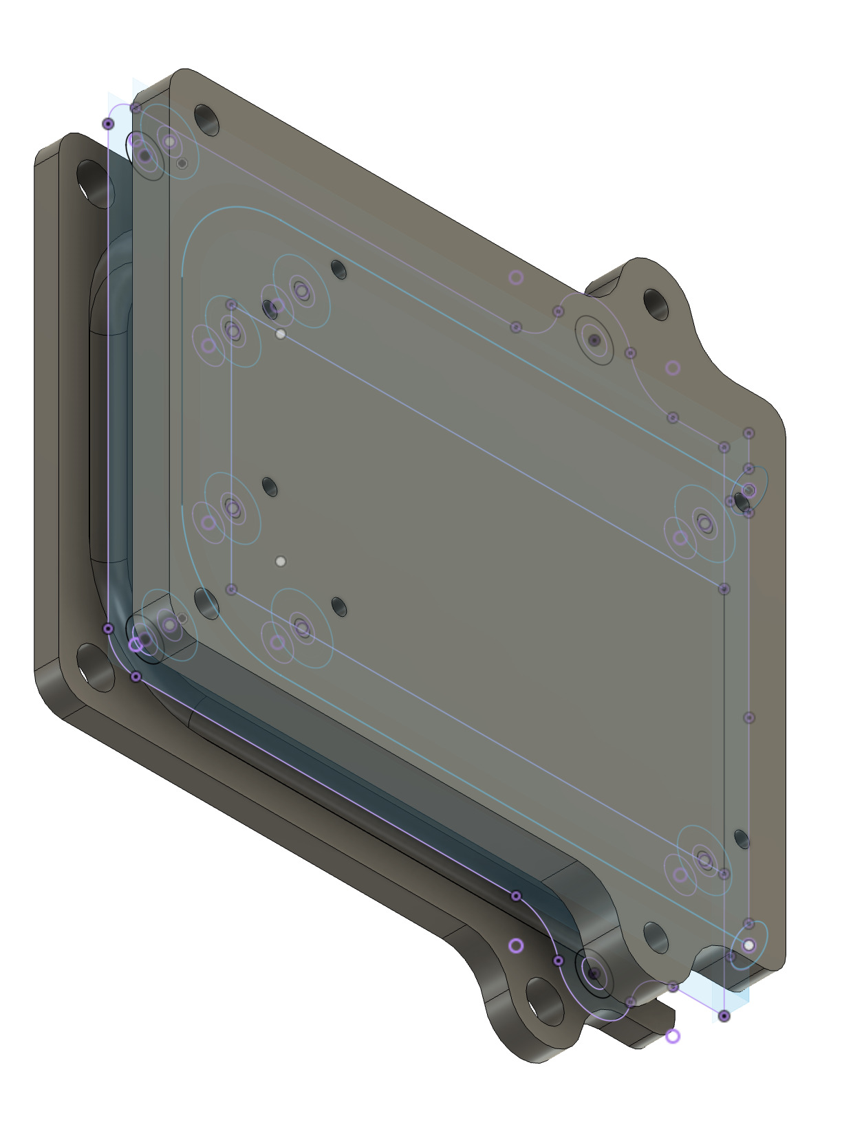
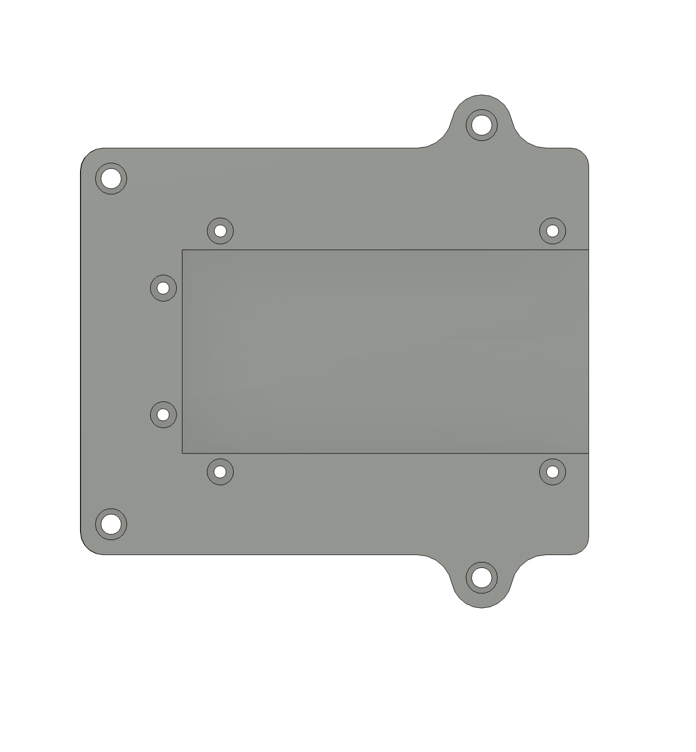
This week, I aimed to target a PCB board that contains a few targeted
components for my final project, namely:
1. LED Light, which blinks upon introduction to PFAS followed by an output message to the
consumer.
2. Button, which functions to turn on/off the LED light, mimicking a light on a potential
LFA detector or filter.
3. Microcontroller, XIAO RP2040, which will eventually have to be upgraded to a ESP 32, in
order to allow for Bluetooth wireless, quantitative sensing readouts.
4. Connector for further incorporation of output devices including resistivity sensor,
Bluetooth.
Circuit Board Design -Tune Ups
I targeted my circuit board design in Fusion 360, Eagle and particularly included a
connection from the button to the LED light, to further encourage connection. It is
important to note, that the class “fab” component folder needed to be downloaded to allow
access to components available in CBA. The design of my board for this week, while
containing additional needed space, was a heart. I will note that the original design from
Week V. was modified to include a connection from LED to the button. From here, I downloaded
the STL files of the top PC board and outline with Anthony’s line of code, “run
singleImages,” which prompts a download of the STL files in Fusion. I then uploaded both my
outline and top file to Neil’s MODS by selecting program PCB 2D Mill feature, followed by
prompting trace outlines for the top and outline, with the following settings:
Top Trace
• Diameter of Mill Screws = 1/64”, 0.4 mm
• Cut depth = 0.1mm
• Max depth = 0.1 mm
• Offset number = 2
Edge Cut File
• Diameter of Mill Screws = 1/64”, 0.8 mm
• Cut depth = 0.6mm
• Max depth = 1.8 mm
• Offset number = 3
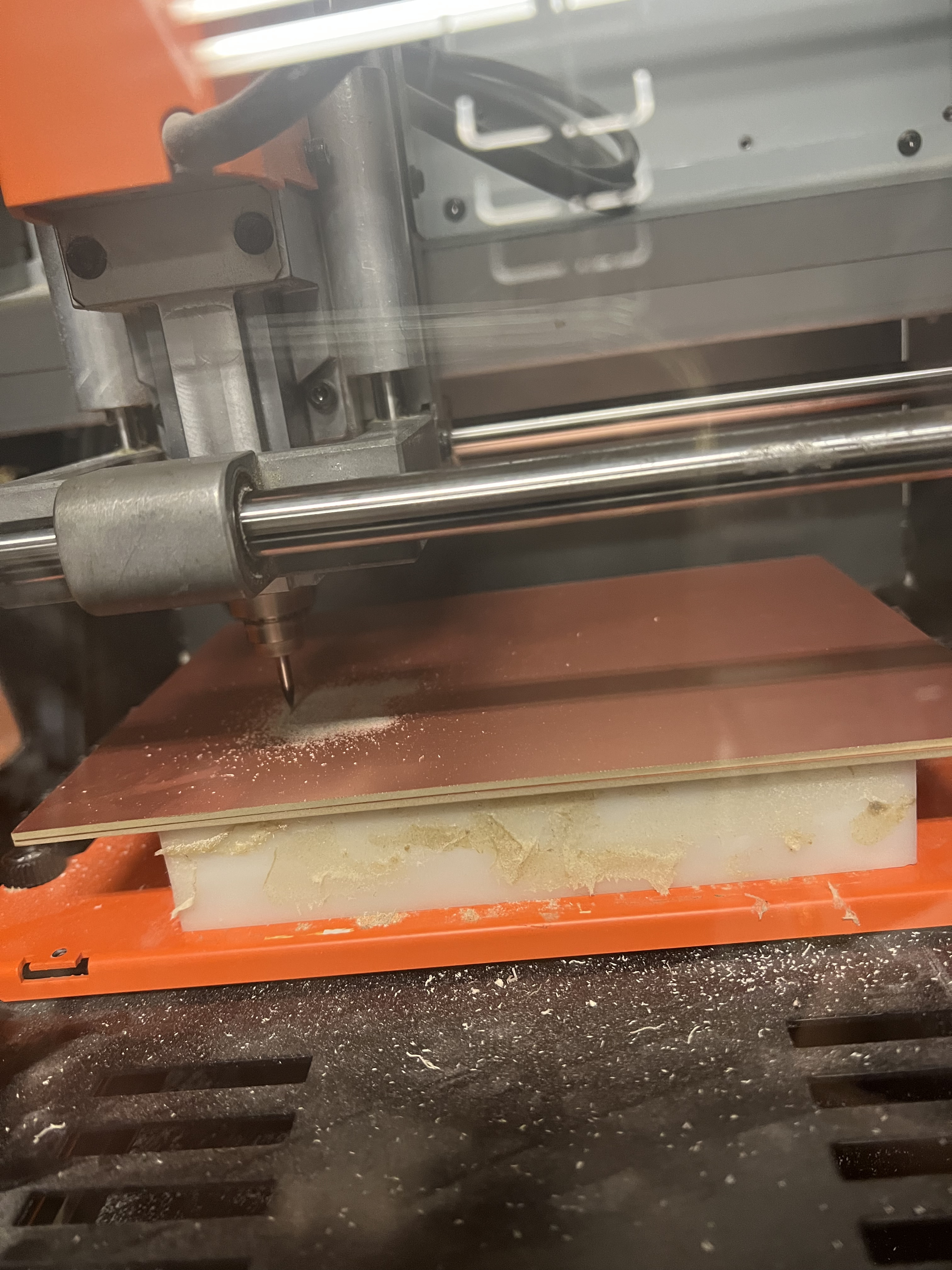
Milling the Board
The program employed for board miling was the Universal G Code software. First, the
appropriate screw was fastened after raising the z axis and removing the vacuum adaptor.
From here, zeroed the x, y, z plane and loaded the top trace g-code file. It is important to
note that during my first trial of milling my PCB board, a major hurdle faced was first
connecting the mill to the software with the guidance of Alfonso and Quentin. In addition,
the trace of the path was originally set to 6 ml diameter, which led to quite unusable mill
jobs. Thus, I further went on to employ a 16 ml route size, which led to a quite pristine
board below:
Soldering Fun
From here, I embarked on the next stage of the project, soldering, following the training
from Alfonso! For this, I employed the tin metal wire, and carefully positioned my component
onto the board. The soldering pen does reach to a temperature of 400 degrees Celsius, so
extreme caution was employed. It is important to note, that the data sheets helped to
indicate the directionality of the LED, Button, and resistors. While I am still working to
finalize the working- product, I have made the following progress shown with the components
below:
2 X 3 Header SMD
10 Ohm Resistor with 5V supply voltage and 3V forward voltage
XIAO RP 2040 Microcontroller
Red LLED1206
SW Switch Tactile 6MM

Molding and Design
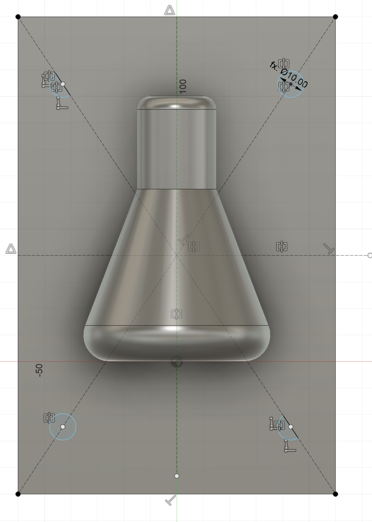
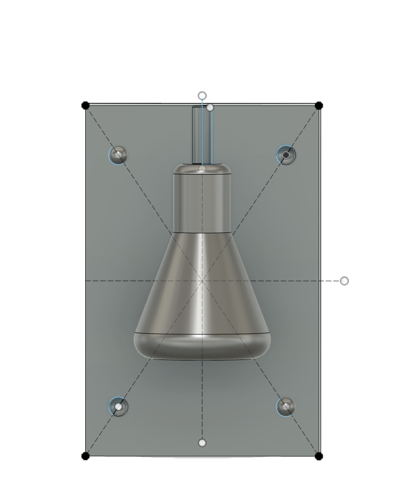
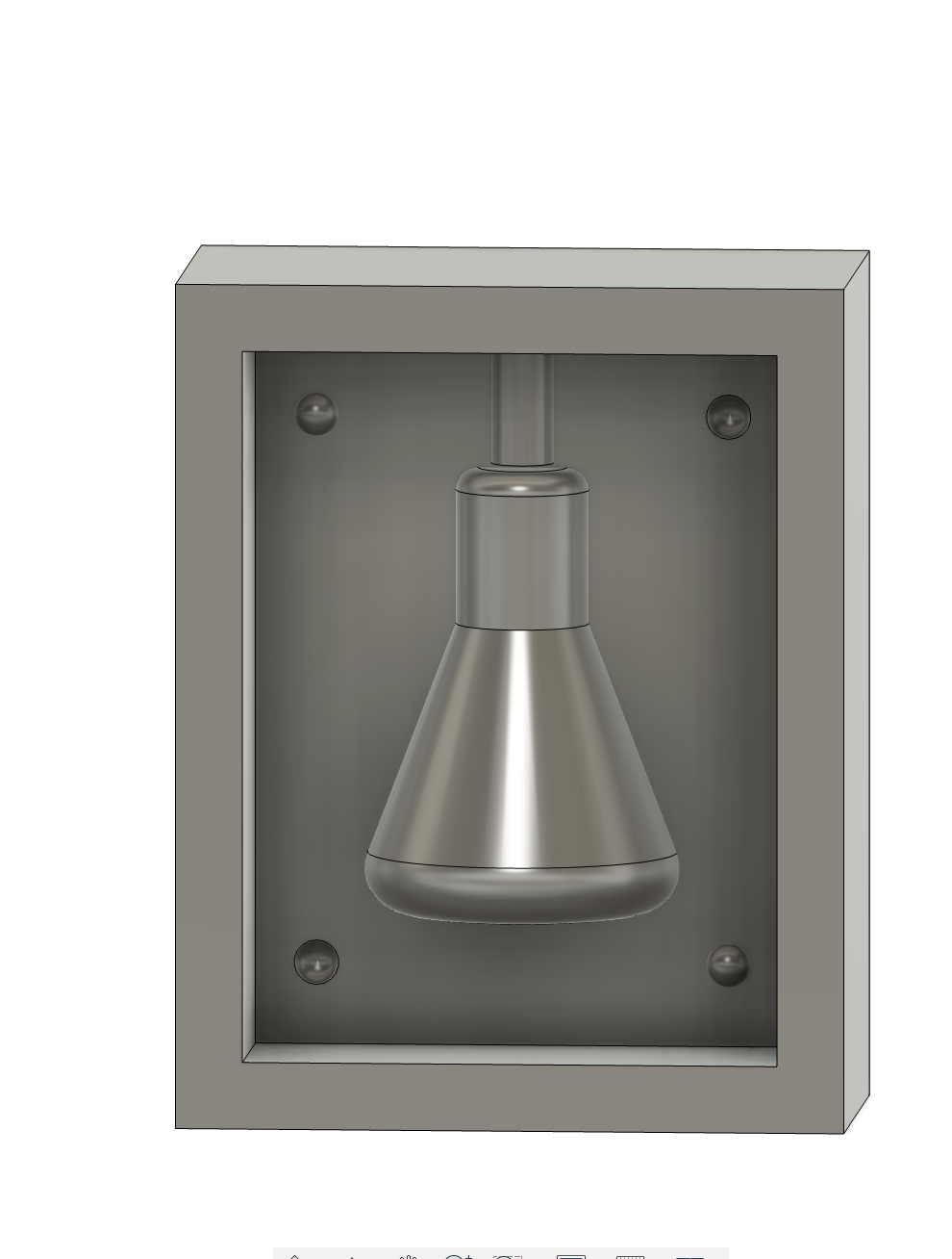
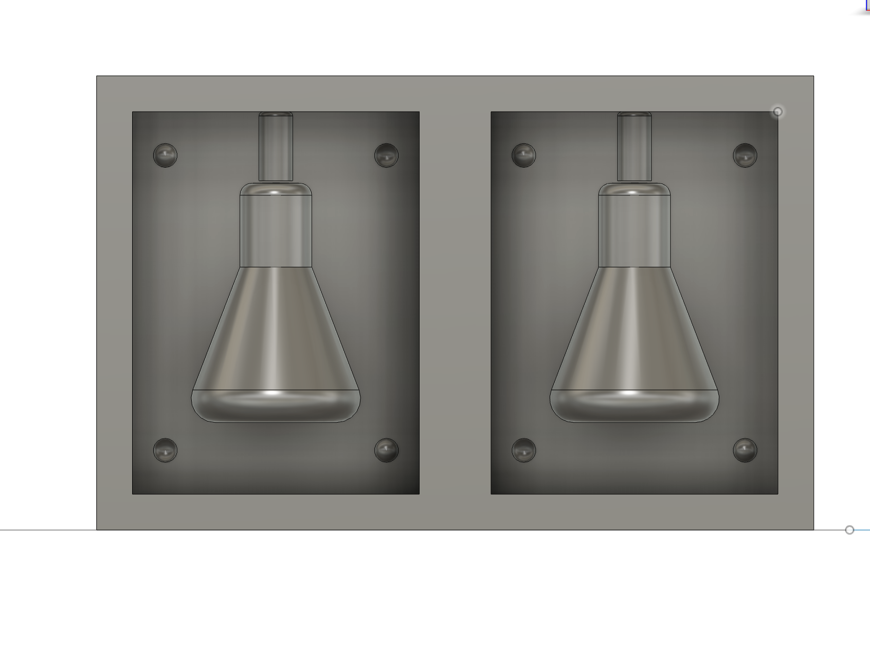
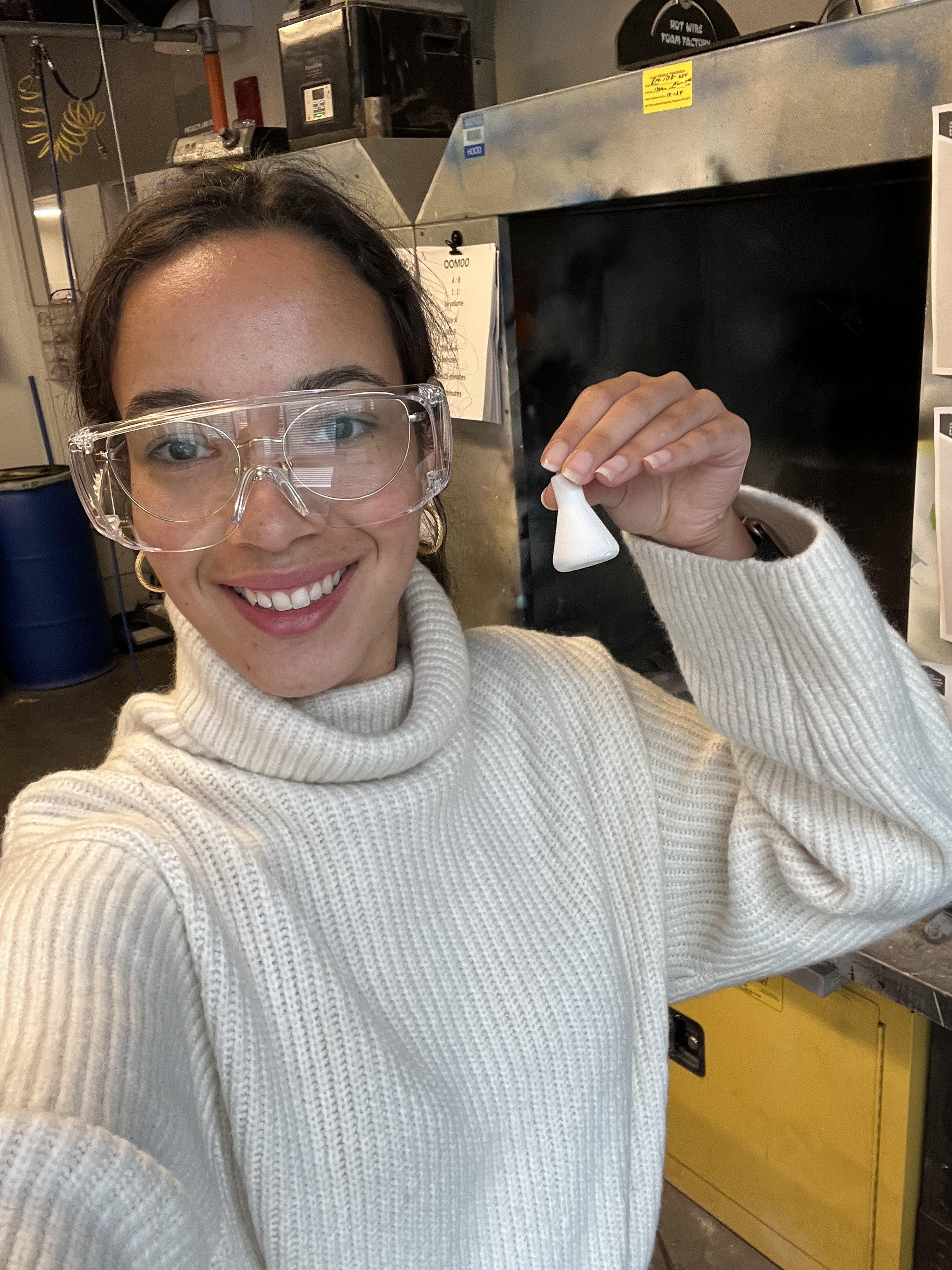
This week, I aimed to design an Erlenmeyer flask for both design aesthetic and to eventually
expand to a food mold for Erlenmeyer candies after the food-friendly silicone material
arrives. To first design the mold, I employed Fusion 360. It is important to note that
parameterization was a key component in order to keep track of all different component
parameters and change them as needed.
I first employed the revolve featured of half of the Erlenmeyer flask drawing, along with
the fillet-feature to smooth the edges. From here, the sketch was extruded with the
revolving feature. Next, I targeted a register with a depth of 40 mm, with length and width
160 mm x 180 mm respectively. Further, tightening, I employed spheres along the diagonal
axes of the mold to encourage fastening when adding the material for the final product.
Moreover, a sprue opening was employed as an outlet to add the material. I do wish that I
had employed a vent, in order to prevent bubbling. Then, to make two molds, I copied my
first mold and then combined both molds to one body. The final mold was exported as a mesh
STL file.
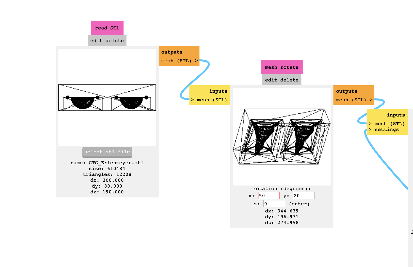
Milling Mold Outline
Cut 3D Software was employed in order to prepare mill trace from the mesh STL file for
milling the wax block. The following parameters were used:
• HTMAA Mill Diameter = 0.125 in
• Pass Depth = 0.1 in
• Stepover = 0.015 in
• Spindle Speed = 6000 rpm
• Feed rate = 90.0
• Plunge Rate = 90.0
• Rapid Clearance Gap = 0.2 in
It is important to note that a smoothing feature allowed for a clean finish. The x and y
axis were then zeroed with the Shop Bot software, following the z axis zeroed with a z-zero
plate. The mold was then milled with frequent vacuum to remove the wax.
Preparing Mold and Casting
I prepared the physical mold with Smooth-On silicone based polymer, with structure described
below. Equivolumes of curing agent A and B were employed at 8 each, respectively. It is
important to note that in preparation a consistent and slow stirring is needed in order to
prevent bubbles from the exothermic reaction. Bubbles that formed on the surface were
removed via sonication. From here the mold curing time for the mold was for 75 minutes.
From here, Hydrocal (gypsum cement) plaster material, which consists of calcium sulfate
dihydrate. A 2.2:1 ratio of Hydrocal powder to water were combined and then stirred slowly
to yield a smooth consistency. From here, the plaster was added to the mold slowly in order
to prevent bubbling. It is important to note a sand bath was used to secure the mold in
place. (Thank you, Graham!)
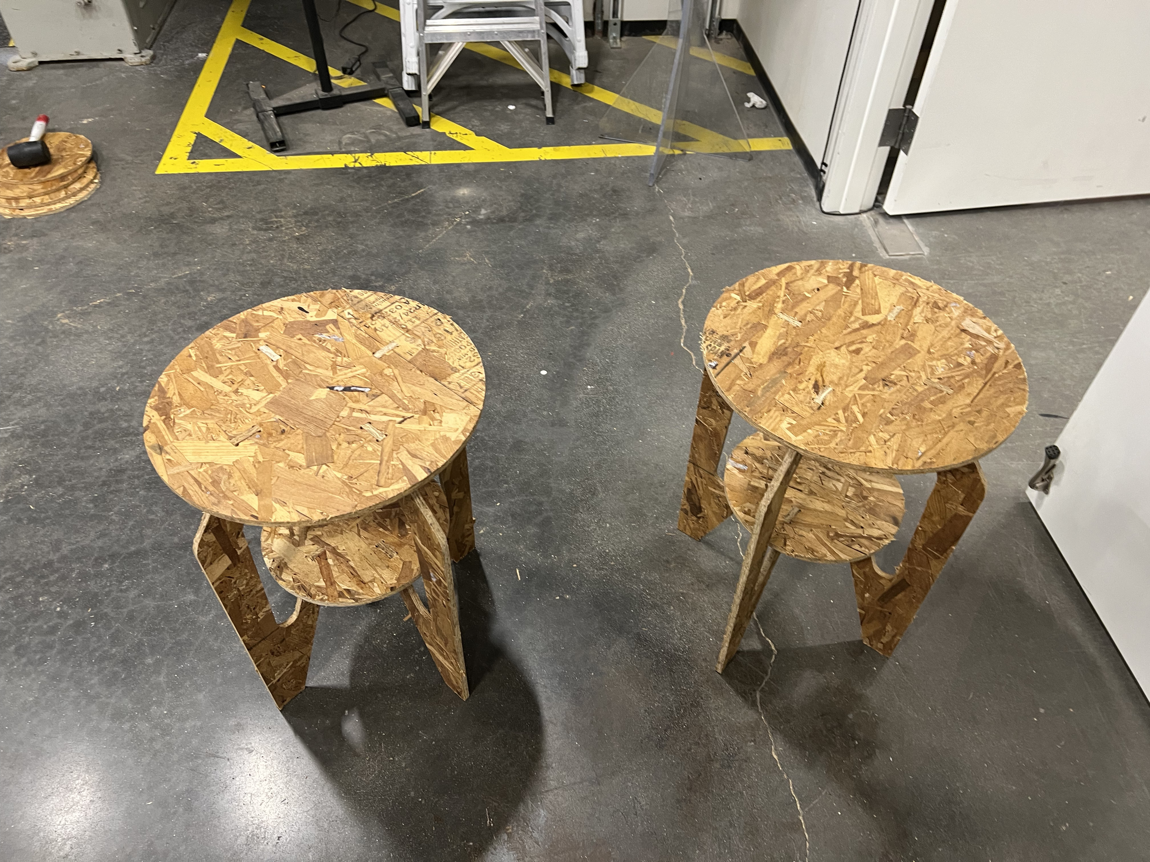
With much anticipation, I was excited to embark on this week’s project
to employ computer-controlled machining to design, mill, and assemble a large piece!
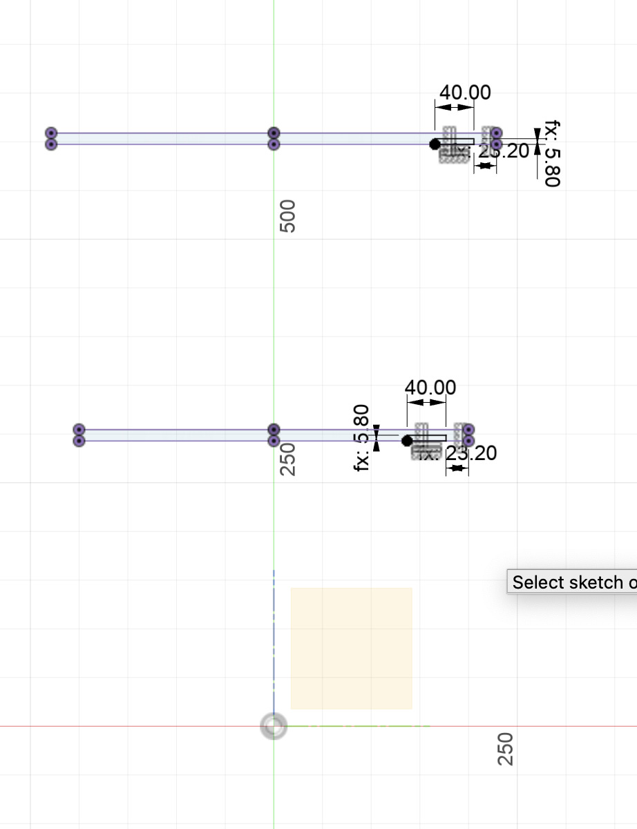
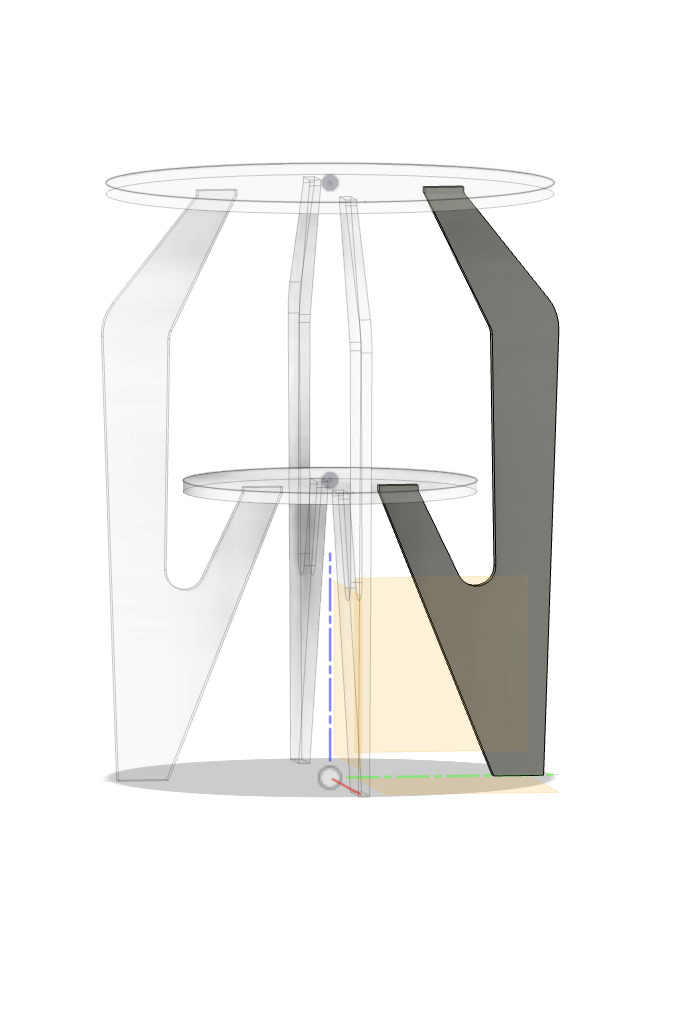
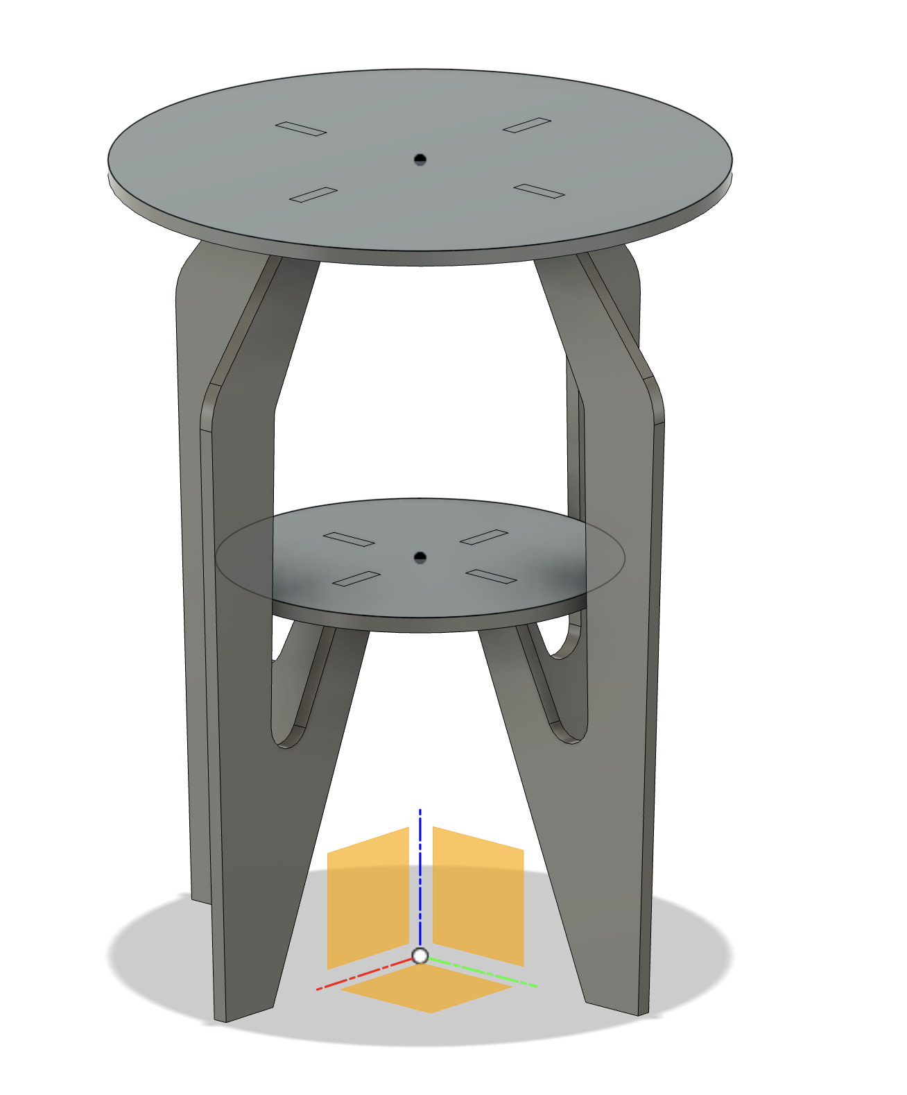
With an interest in tables for my apartment décor, I set out to design two-tiered
nightstands. In my design phase, I first considered a circular base and top shelf, along
with modern legs below. My ideal height for the nightstand would be 24 inches.
Design
First, I spent much time on YouTube to learn the general design assembly process for
Fusion 360 furniture parts. Next, I embarked on the design phase by measuring the
thickness of the wood at 11.6 mm with 4 ft x 8 ft width and length, respectively. To
start, I defined the parameters of my drawing, through the parameterization feature:
Thickness = 11.6 mm
Height = 609 mm
Top Shelf Diameter = 457.2 mm
Bottom Shelf Diameter = 300 mm
Length of Base = 8 ft
Width of Base = 4 ft
Next, I first began by defining an offset construction plane with the height of the
table. This encouraged the three-dimensional drawing, assembly, and modeling of my
piece. From here, I began drawing the top shelf on the offset plane with the height of
the bottom shelf. Note, after drawing followed by extrusion to the wood thickness of
11.6 mm. Similarly, I defined the offset plane height (parameterized as height/2) for
the bottom shelf.
The leg of the chair could then be drawn by drawing on an
offset plane perpendicular to the shelves. It is important to note, that a feature of
circular pattern was then employed along the z-axis to yield 4 legs of the table.
Lastly, I targeted cuts within the top and bottom shelf for assembly through the combine
and cut feature. From here, a new base of the BCX plywood board was targeted with 4 ft x
8 ft dimensions, and the joint feature was employed to add each piece of the table to
the base. A dxf file was then exported.
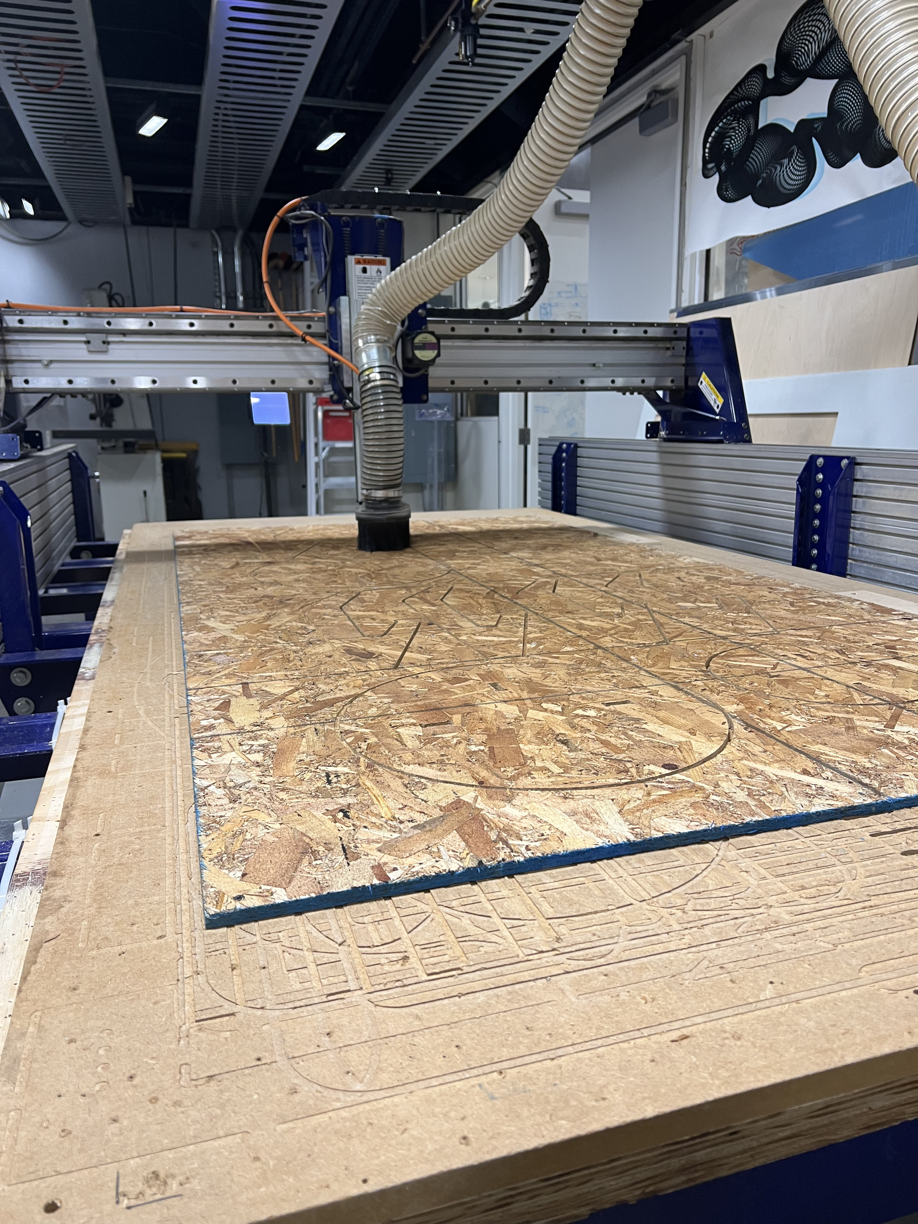
The VCarve program was employed with a defined 96 in by 48 in dimensions. Thank you to
John for training and guidance! It was important to not employ the offset feature and
ensure that 2 in margins were considered to account for screwing the wooden piece in
place. From here, the join and close vectors feature was utilized to ensure each piece
was closed. I then added the dog bone features to the slots along with tabs.
Stock Cut Thickness = 0.52 in
Depth Cut = 0.26 in
Conventional Cut (clockwise from L to R)
Endmill = 0.25 in
Next, the toolpath was defined to yield the ShopBot file for milling followed by export
to the ShopBot file.
Milling
The ShopBot Mill was employed to mill the design. It is important to note that PPE (long
pants, goggles, close-toed shoes) is necessary when working with the ShopBot and
assembling designs. In addition, a filter vacuum was utilized to collect sawdust
particles.
First, the ShopBot file was opened, and the and y zero were previously defined. Thus,
the z zero was defined with a z zero metal plate. Upon zeroing in all three dimensions,
it is now time to start the spindle by pressing the green button, start. The milling
process lasted approximately 30 minutes.
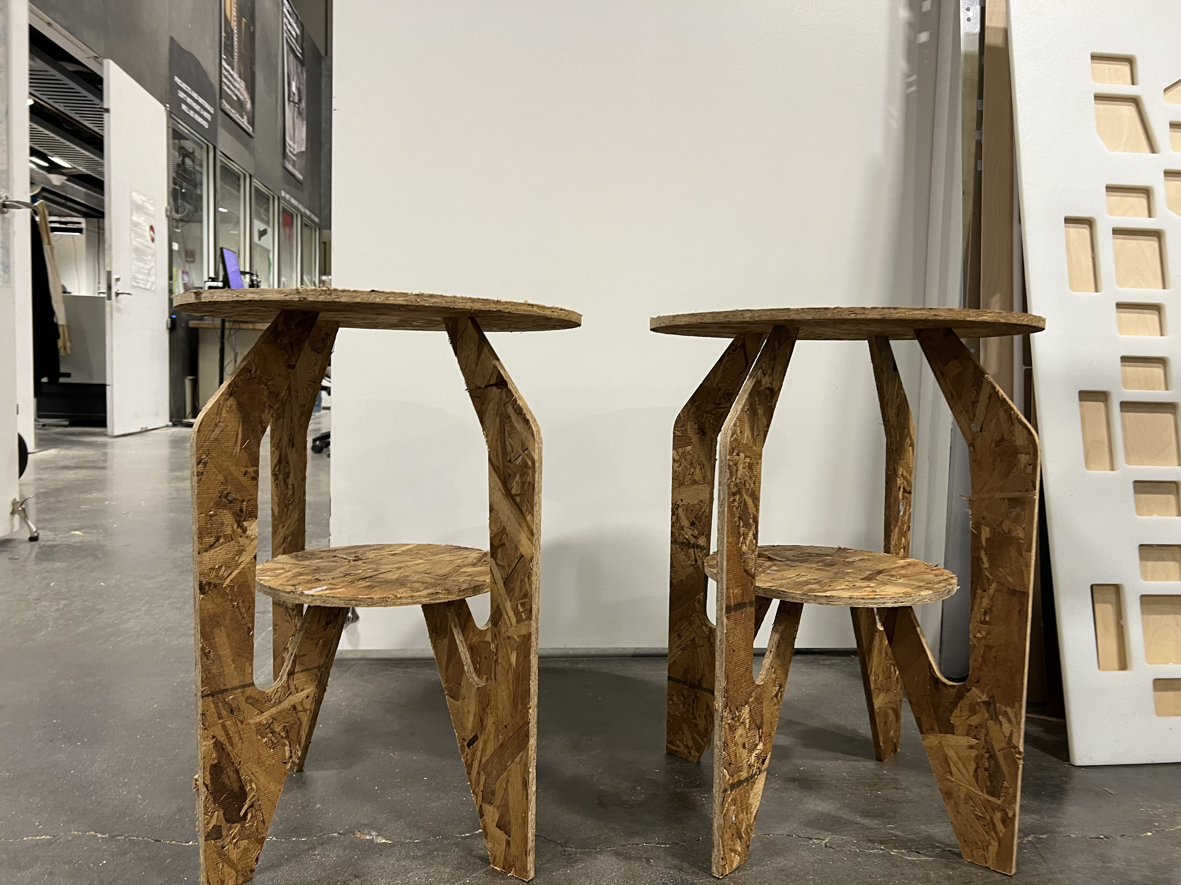
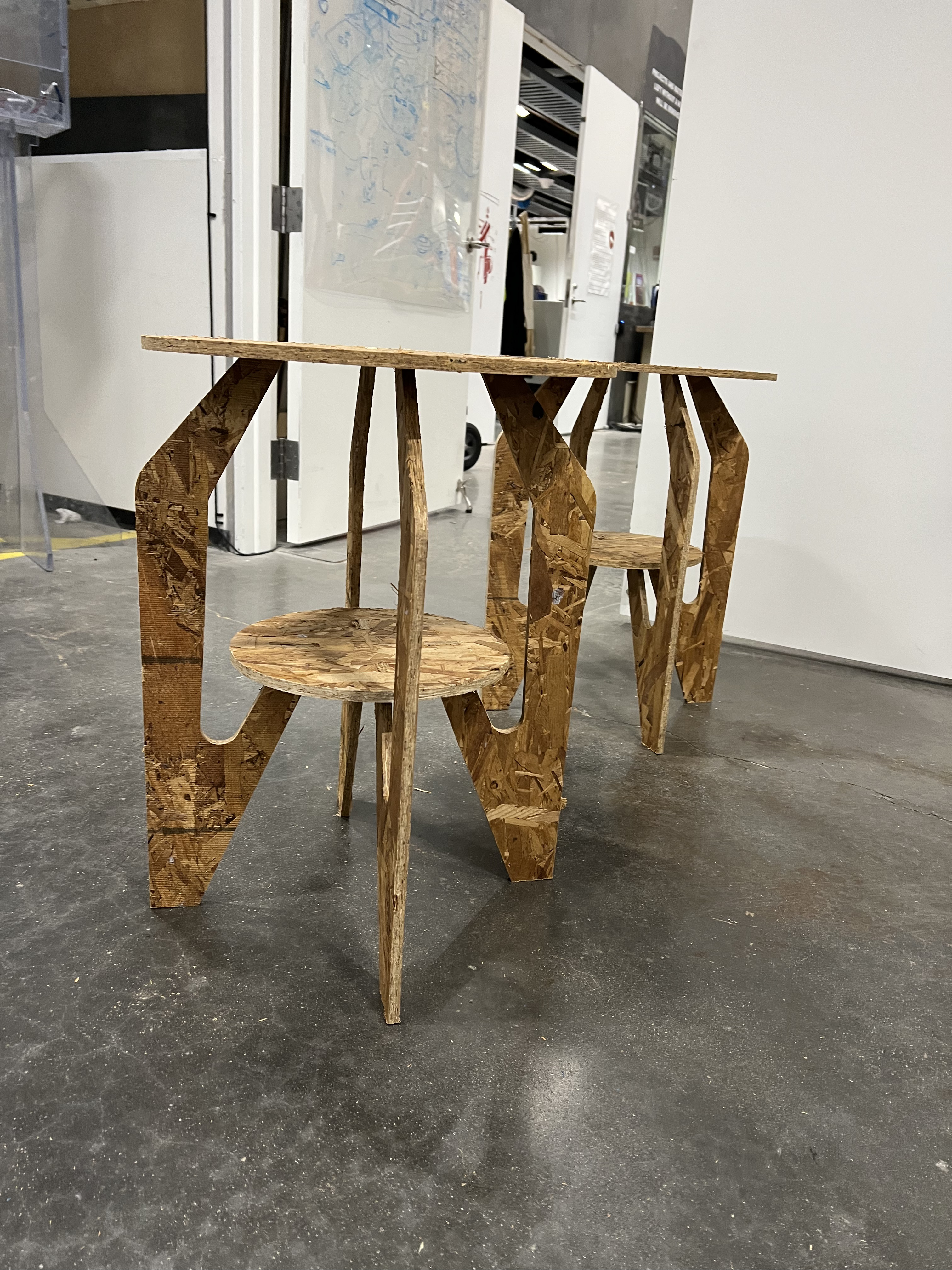
Assembly
Initially, when assembling my table, the bottom shelf assembly cuts did not adequately
scale with the size of the top table cuts. Thus, I milled the bottom shelf design.
Editing the cut slits to yield my exciting masterpieces below! Overall, I enjoyed this
week’s project design and look forward to targeting my tables with more durable wood
later this week.
With a strong interest in building on my final project, I was eager to
embark on input design this week. With an interest in monitoring the conductivity change
of my conductive polymer films upon introduction to PFAS in order to further quantify
the concentration of PFAS, I was eager to design an input device to record the
resistance of my polymers.
Design
In order to design my PCB board, I employed Eagle in Fusion 360 Software. The Xiao RP
2040 Microcontroller was employed with particular interest in the A0-A3 ports for input
sensing of the resistance. As I monitored the resistance with two electrodes, I employed
the A0 port. In order to monitor the voltage of the electrodes over time, a voltage
divider was employed, by which:
Voltage Source = 3.3V
Resistance 1 = 20 MOhm
Resistance 2 = 10 MOhm
Output Voltage = 2.475V
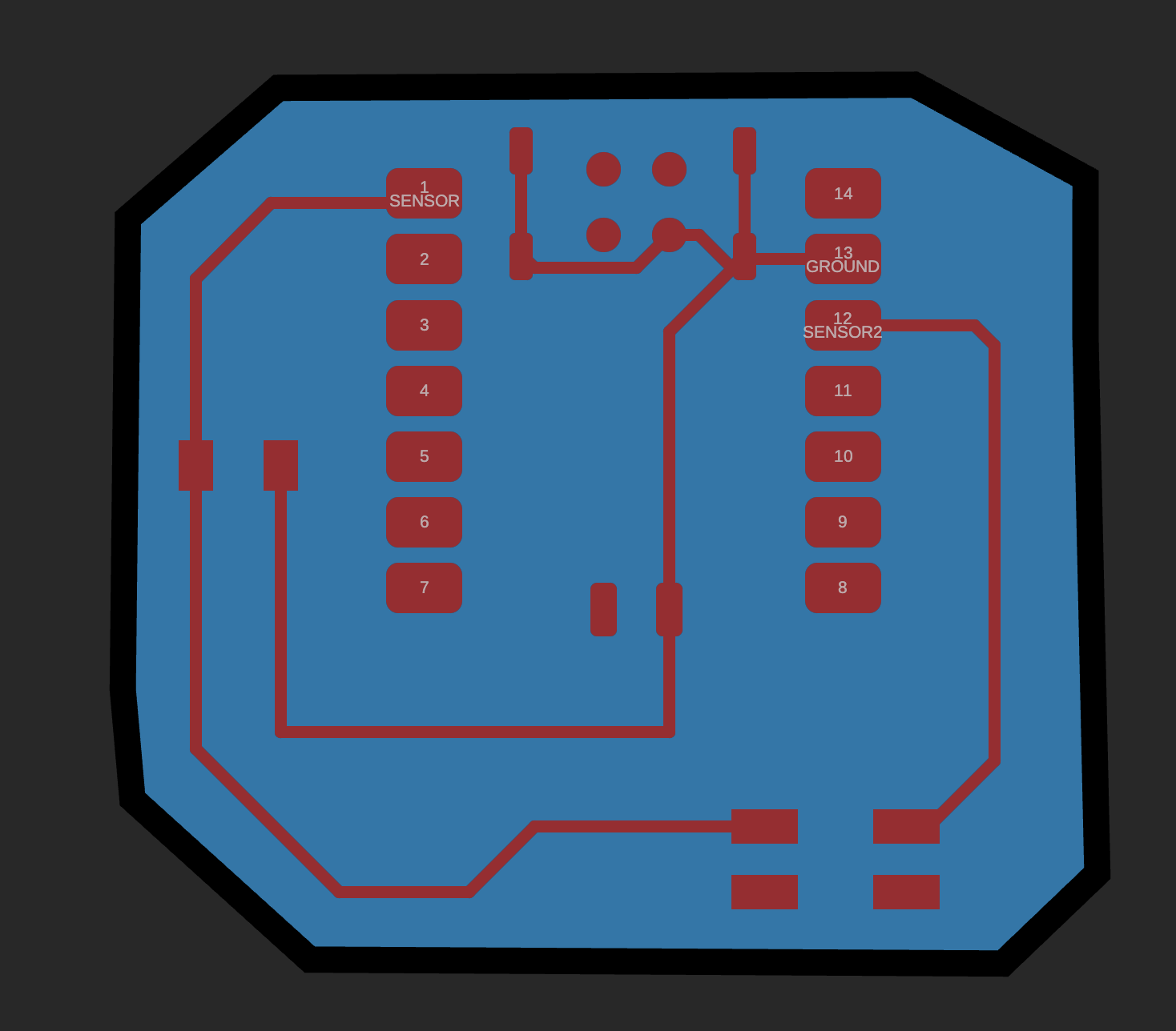
Milling and Soldering
The SRM-20 Roland was employed to mill the PCB Board, which was controlled directly
through MODs. For the SRM-20 Roland MODS Program, the PNG image must be uploaded to
generate a mill-path instead. It is important to note that the x,y,z zero must be
manually determined. The traces employed were 16 mills, which offered an intricately
milled board at the end.
During the soldering phase, tin metal was employed in order to sadder the XIAO
microcontroller, 10 MOhm resistor, and connector to the board. While I am still
acclimating to soldering, I eventually was able to establish a connection between each
component as confirmed via multimeter detection signals.
Arduino and Input Sensing
For programming the RP Xiao 2040 Microcontroller, I employed Arduino IDE code, by which
I defined the input port for the analog pin as A0, the 3.3V reference, which also can be
referenced to 1024 counts later in the script.
Furthermore, calculations for R1 can be determined from the voltage divider equation:
V out = (Vs*R2)/(R1+R2)
During the sensing phase, I ran the Arduino code and was able to measure the resistance
of the polymer films on the order of 3-4 MOhms, which indicates high oxidation of the
polymer sample, but also doesn't directly align with the 4-point probe resistance of 20
MOhm. Further tuning must be targetted as a background resistance of 1 MOhm was observed
and to yield consistent reading with the four point probe. In the future, I aim to
improve the design of the electrodes through vinyl cutting copper tape designs with
controlled contact to my polymer films.
This week, I at first was quite interested in developing a Touch Screen
Output Device with a TFT LCD Display Touch Screen, but after some analysis on the
complex microcontroller incorporation and soldering needs, I chose to first target an
OLED SSD 1396 Display.
I then refined my goal to target the readout of the PFOA Concentration within the
analyte along with EPA Limits of detection. A sample OLED Readout would include two
cases:
1. PFOA Concentration is above EPA Limits:
“Alert! PFOA Concentration = 200 ppt. Warning! Above EPA Limit of Detection.”
2. PFOA Concentration is below EPA Limits:
“Alert! PFOA Concentration = 0.03 ppt. Below EPA Limit of Detection.
In order to target my wireless readout of PFOA Concentration, I first targeted my PCB
Board with an Xiao RP2040 Microcontroller. In designing my PCB Board, on Fusion 360
Eagle, I solely targeted to incorporate my RP2040 Microcontroller along with a connector
to the OLED Display. Important connections to the OLED Display included:
GND: Ground
VCC: Voltage at Common Collector is the power supply which ranges from 3.3V - 5.0V
SCL: Serial Clock Line, which is a digital communication signal for data transmission.
Moreover, the Serial Clock Line also confirms that the receiver (microcontroller and
OLED) and sender (Arduino Code) receive communication at the synchronously. Note, the
SCL and SDA are both employed in the I2C (inter-integrated circuit) communication
protocol, which carried data.
SDA: Serial Data Line, which works with the SCL and allows for data to be communicated
between devices.
Milling
From here, I went on to embark on a long journey of milling. While, I was relatively
content with the simplistic function of my board, I ran into some time demanding milling
troubleshooting experiences including:
• Worn out end mills.
• Origin recognition issues on the SRM 20 PCB.
• Leveling and zeroing.
I am extremely grateful to Alfonso and Quentin for helping me in the milling process.
Thank you Alfonso for going through a review milling process with me, I appreciate it.
Soldering
The fun continues! I went on to solder my board but noticed a light spark in copper
traces upon milling the connector component. I attribute this to potential component
failure of the connectors or the melting of the copper traces. Upon attempting to
connect my computer to the board with an HDMI, I could not observe any light flashing.
Upon attempting to boot and reset the board, I still did not observe a light flicker. I
went on to carry out examination with a digital multimeter to determine if current did
flow through the copper traces, but unfortunately could not observe current near the
adaptor. Despite a time-demanding week, I emphasize a few key learning points:
1. The connections incorporated within an OLED and the RP 2040 microcontroller allow for
communication from the Arduino code to the OLED Device via an output function with the
inter integrated circuit (I2C) communication.
2. It is important to make a thorough analysis of milling conditions to prevent an over
exhaustion in milling time. (6 hours.)
3. One can spark a circuit through soldering, and it is important to always maintain a
safe working environment. Including an exhaust fan, tweezers, and caution when handling
the soldering pan. Please read SDS sheet before handling the soldering pen.
I did manage to write my Arduino Code for the OLED readout with reference to and hope to
further incorporate my output device into my final project.
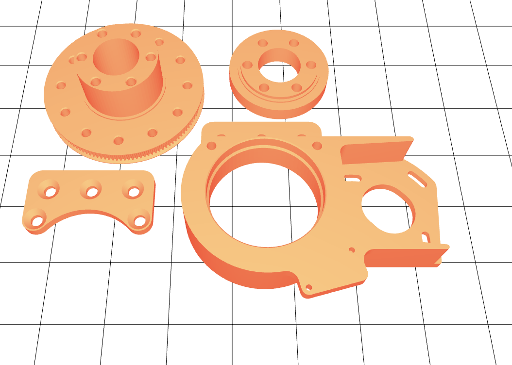
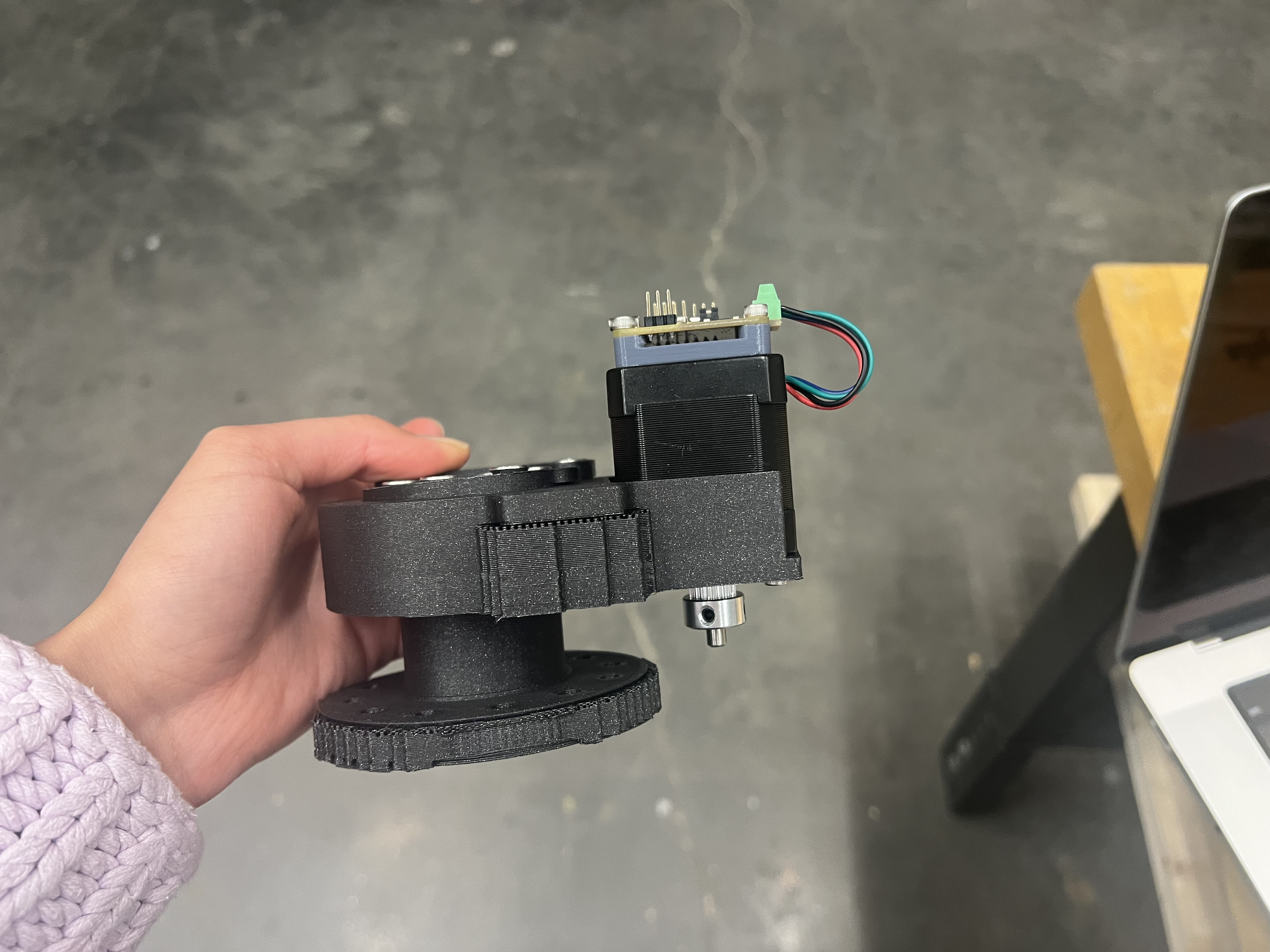
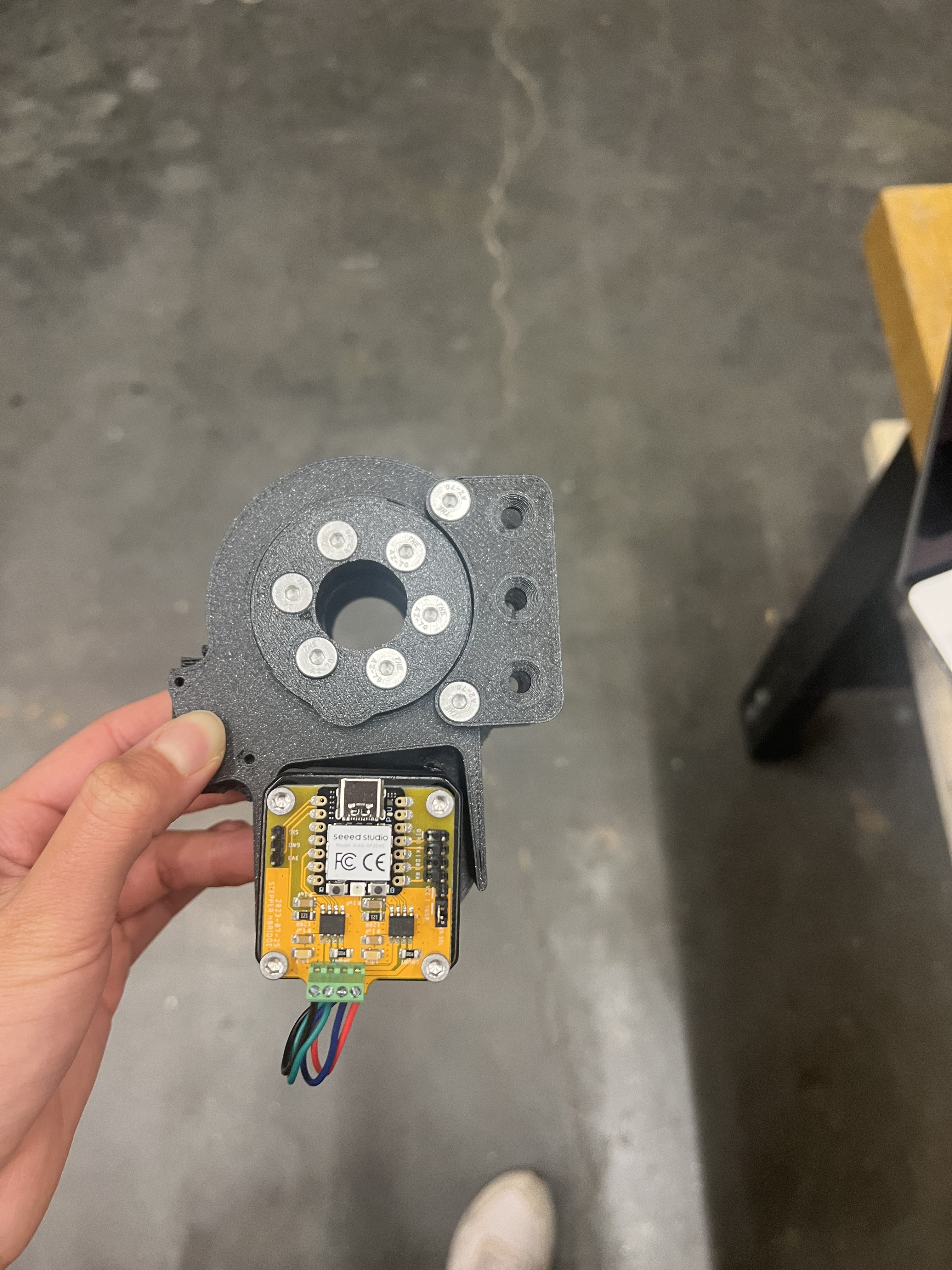
For machine building week, my CBA section aimed to build a camera
machine for monitoring photos. I contributed to the team project by 3-D printing, and
assembling the rotor employed for synergistically rotating the models in front of the
camera. This model incorporates a PCB board with a XIAO-RP2040 microcontroller in order
to further connect the rotor to a step motor for rotating the models on a platform.
Find out more about our group project below:
https://fab.cba.mit.edu/classes/863.23/CBA/machine/index.html
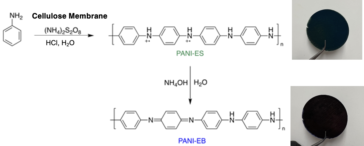
In the sphere of materials
synthesis, I targeted the interfacial
polymerization of polyaniline(PANI) nano
fibers for my final project. The beauty of
PANI coatings is that they exhibit a rigid
conjugated backbone, which allows for facile
oxidation to the emeraldine salt upon
acidification of PFAS.
This polymerization is carried out with an
oxidant, ammonium persulfate (APS) and
camphorsulfonic acid (CSA), and
Dichloromethane. Upon polymerizing
polyaniline to yield the emeraldine salt
form, the PANI-ES was reduced to PANI-EB
with ammonium hydroxide.
While PANI-EB is insoluble in most organic
solvents aside from DMF, it can be characterized
by Scanning Electron Microscopy (SEM), Fourier
Transfer Infrared Resonance (FTIR) Spectroscopy,
and Thermal Gravimetric Analysis. The
degradation temperature, Td of PANI was
determined to be 326.12 °C.
As PANI forms even dispersions in aqueous media,
it can be employed as an ink for the lateral
flow assay sensors. In addition, PANI can be
polymerized homogeneously on cellulosic
membranes for the filter sensing devices. This
encourages controlled, rapid, and limited-waste
preparation of PANI-paper for further
commercialization of the PANI devices.