## Electronics Production
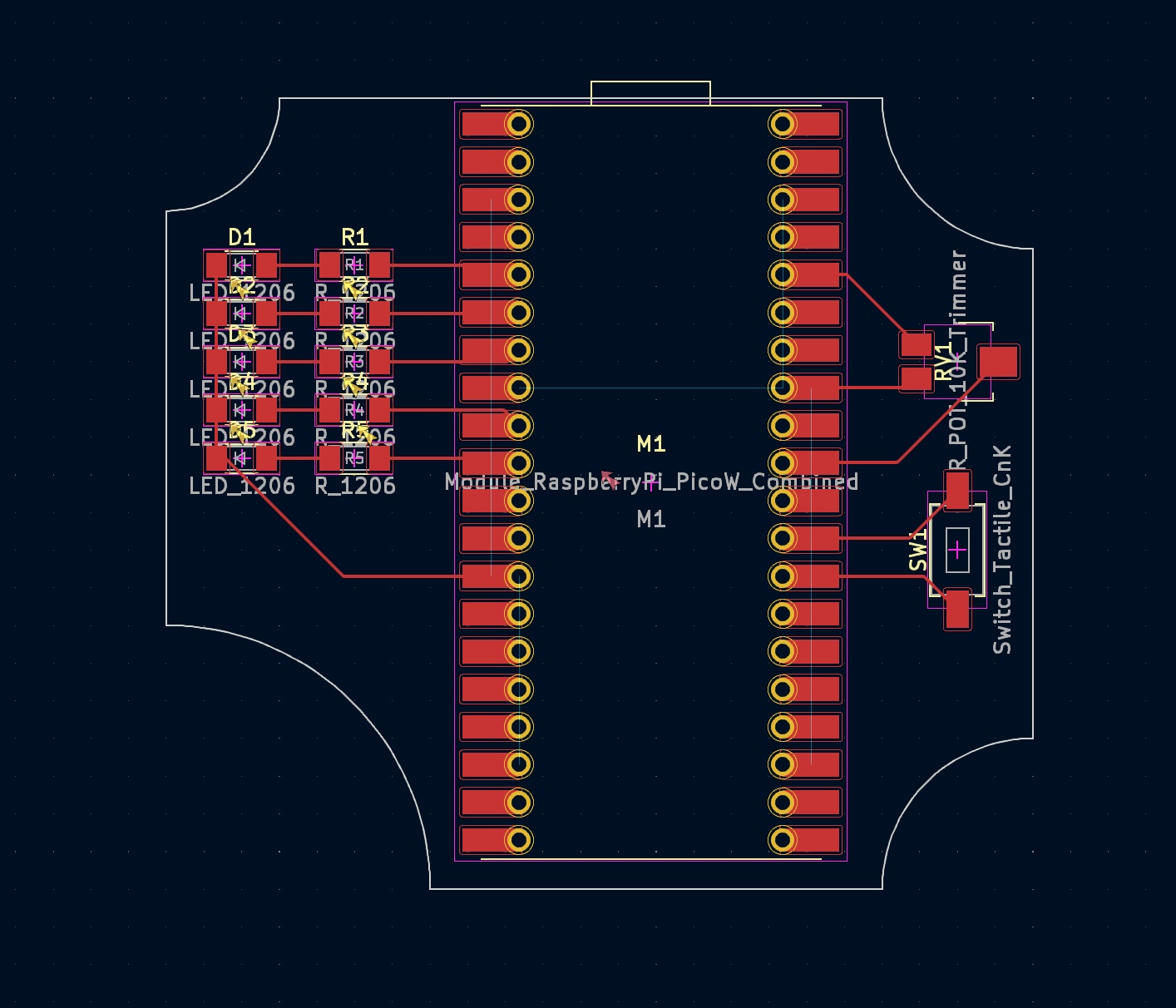
I decided to mill the PCB I made for electronic design week. Here is the design for recap:
I followed the following workflow to mill the PCB:
- Export the kicad pcb design as a gerber file.
- Convert the gerber file to a png file using Quentin's tool .
- Import the png file into the mods program to mill 2D traces and edge cuts.
- Use the UGS platform to mill the PCB. First manually determining the x=0, y=0 coordinates and then running the macro function "probing and zeroing z".
Little did I know that this was not going to be so straight-forward. I ran into issue with the "probing and zeroing z" on the pcb milling machine not working. After talking to a few people in class, I realized that this was a shared problem so I posted an issue [here](https://gitlab.cba.mit.edu/classes/863.23/CBA/cbasite/-/issues/12).
After manually determining the z=0 coordiante, I tried many times to get the PCB to mill correctly. The first time I ran 4 passes to get the traces on the right hand side.
Here is the first time I ran the mill going over the passes over 4 times to get the right hand side:

I then decided to start afresh on Tuesday to mill my PCB and again the same thing happened. Office hours were super helpful and I got Alfonso's help to fix the level bed issues. He came up with a super useful mechanism to fix the copper boards on top of acrylic board and double-tape the copper board on to another sarcrificial board. Here is the new process detailed in this [issue](https://gitlab.cba.mit.edu/classes/863.23/CBA/cbasite/-/issues/14).

The second failed try - I considered using a knife to mill the remaining traces but faced another issue with the edge cuts not lining up with the milling traces and this made my board unusable :((((( I had followed the workflow of exporting my kicad pcb_design as a gerber file. When converting the gerber to a png file using Quentin's tool , I kept the x and y origin coordinates the same. My best guess for why this could have happened is while inspecting and debugging the curved copper stock issues, we disturbed the origin coordinates.

Thanks to Alfonso, a lot of failure boards were saved and I could finally mill my PCB on early Wednesday morning!
How it is going:

Ah what a wonderous day it is today!

Soldered the board which proved to be harder than I thought. Miana was super helpful in helping me learn how to solder the board and Alan provided me with hands-on help by checking my traces and showing me how to solder small parts.
Soldering the board:
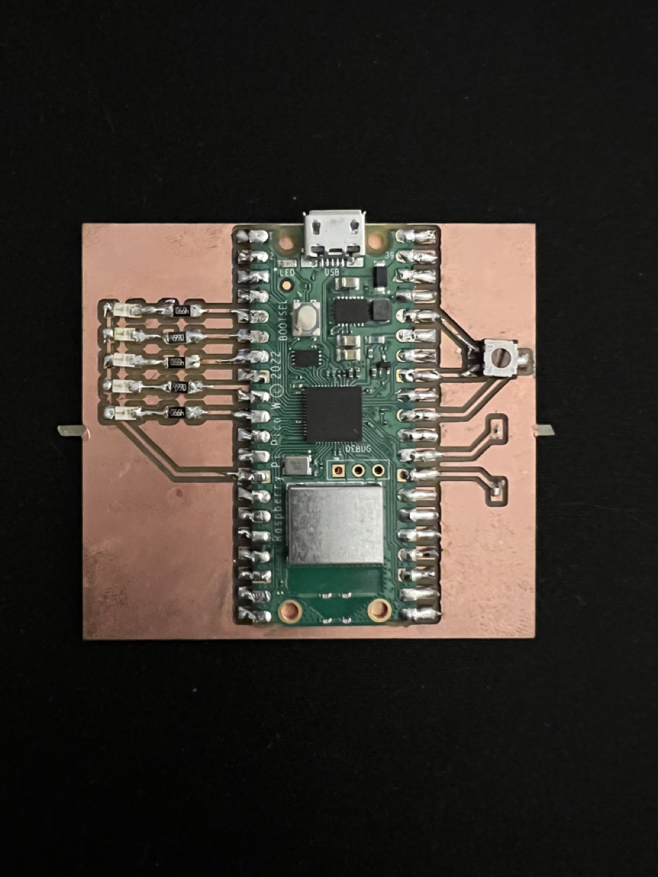
I finally have a working PCB.