How to Make (almost) Anything 2023 | Week 11.1: Networking & Communications
Home
Assignment: Group Project -- Send a message between two projects; Individual Project -- Design, build, and connect wired or wireless node(s) with network or bus addresses and a local interface.
Individual assignment: Design communication network
Description: Re-creation of the HTMAA broad_hop example, exercising the use of double sided boards, design tracing, and multiboard connection
Primary files:
- Networking board1 PCB design and design (KiCad; recreated / adapted from HTMAA broad-hop example)
- Networking board2 PCB design and design (KiCad; recreated / adapted from HTMAA broad-hop example)
- Board1 programming (Python; source: Neil Gershenfeld, HTMAA Broad-Hop)
- Board2 programming (Python; source: Neil Gershenfeld, HTMAA Broad-Hop)
- Board1 communication programming (Arduino IDE; source: Neil Gershenfeld, HTMAA Broad-Hop)
Procedure:
- Following the graphic depicted on the HTMAA website for the Network & Communicatiosn broad_hop example (board1, board2), I re-created both boards in KiCad with modifications to utilize material that was in stock at the lab (primarily repurposing the connectors to be standard pin headers) and utilizing graphical traces
- Once the KiCad file has been made, export as a gerber (note: for board2, it is important to also export the drill file)
- Using the PCB milling machine in EDS, the gerber files were imported to the desktop program (note: given this machine uses a 1/32 end mill for majority of trace milling, increased space is required between traces; as such, the board was revised several times to ensure there were no errors on the narrow traces)
- Once the program is set up, secure the double sided PCB to the bed
- Change the end mill to a blunt tool, then zero the machine along all axes
- Replace the endmill with the 1/64 and initiate initial traces
- When prompted, switch out the end mill for the 1/32 and allow machine to zero and proceed to the next trace
- Upon completion of the step above, the single-sided board1 can be removed from the machine, and the PCB will be flipped over to mill the backside of board2
- Proceed the milling process with the newly flipped over PCB material
- Upon completion, inspect all boards to ensure the traces are clean; In my instance board1 had traces too close together so I scraped away the copper to differentiate the traces and used jumper wires in the soldering process
- Solder the respective components to each board (note: board1 requires jumper wires that should be soldered last; board2 requires rivets for the throughholes, which should be implemented first)
- Upon completion of soldering, inspect the boards to validate there are no shorts
- Connect the boards using connecting cables
- Using Ardiuno IDE and Python, reference the code provided by Neil Gershenfeld on the HTMAA website to load board2 and execute the program across the boards (1, 2, 3)
Key learnings:
- Utilizing vias can be helpful to alleviate congested boards (although a more time consuming process) -- I discovered that soldering tiny components can be frustrating, particularly on a dense board; Considering this, having the backside of the board to run traces helped alleviate a potentially even more dense board and areas where routing was not possible
- If traces aren't working as planned, all hope is not lost -- Given my board had traces that bled together during milling and another instance where the copper peeled, I discovered the world of jumper cables to solve most problems
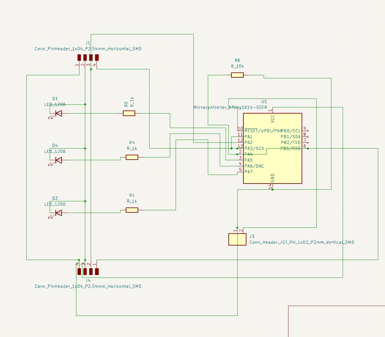
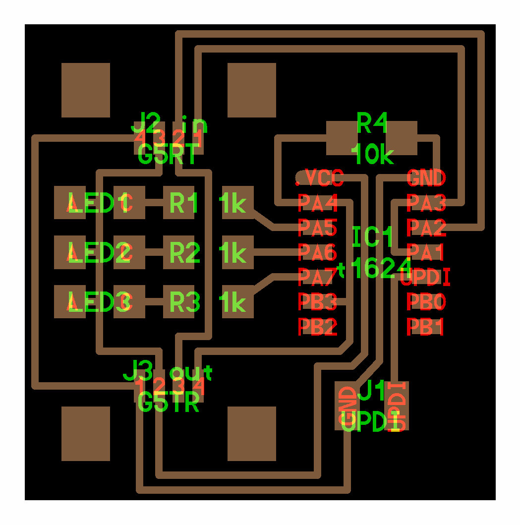
Networking board1: PCB design schematic in KiCad
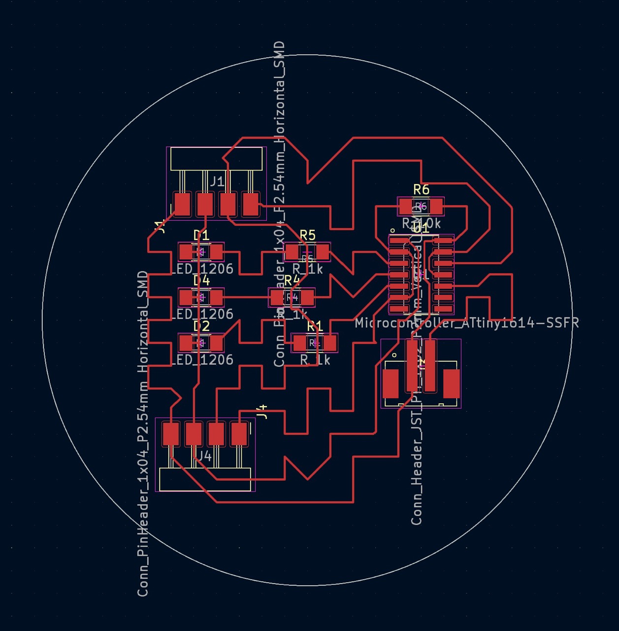
Networking board1: PCB design in KiCad
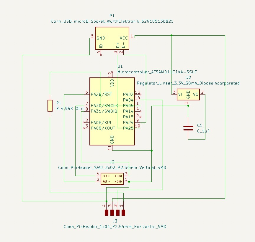
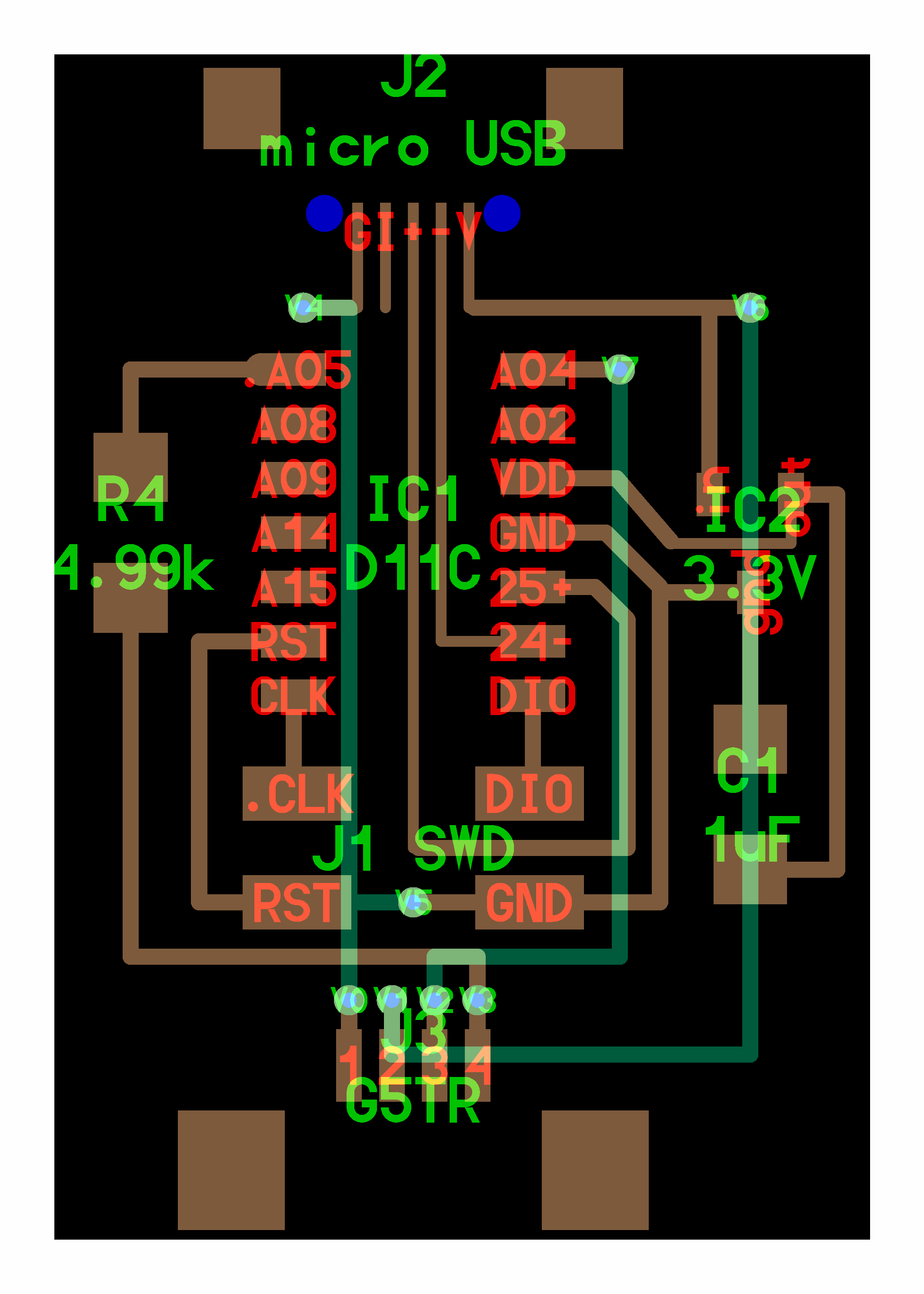
Networking board2: PCB design schematic in KiCad
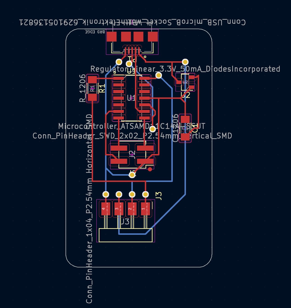
Networking board2: PCB design in KiCad
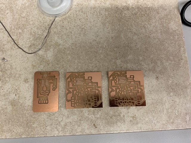
Networking board1 & 2x board2 milled PCBs
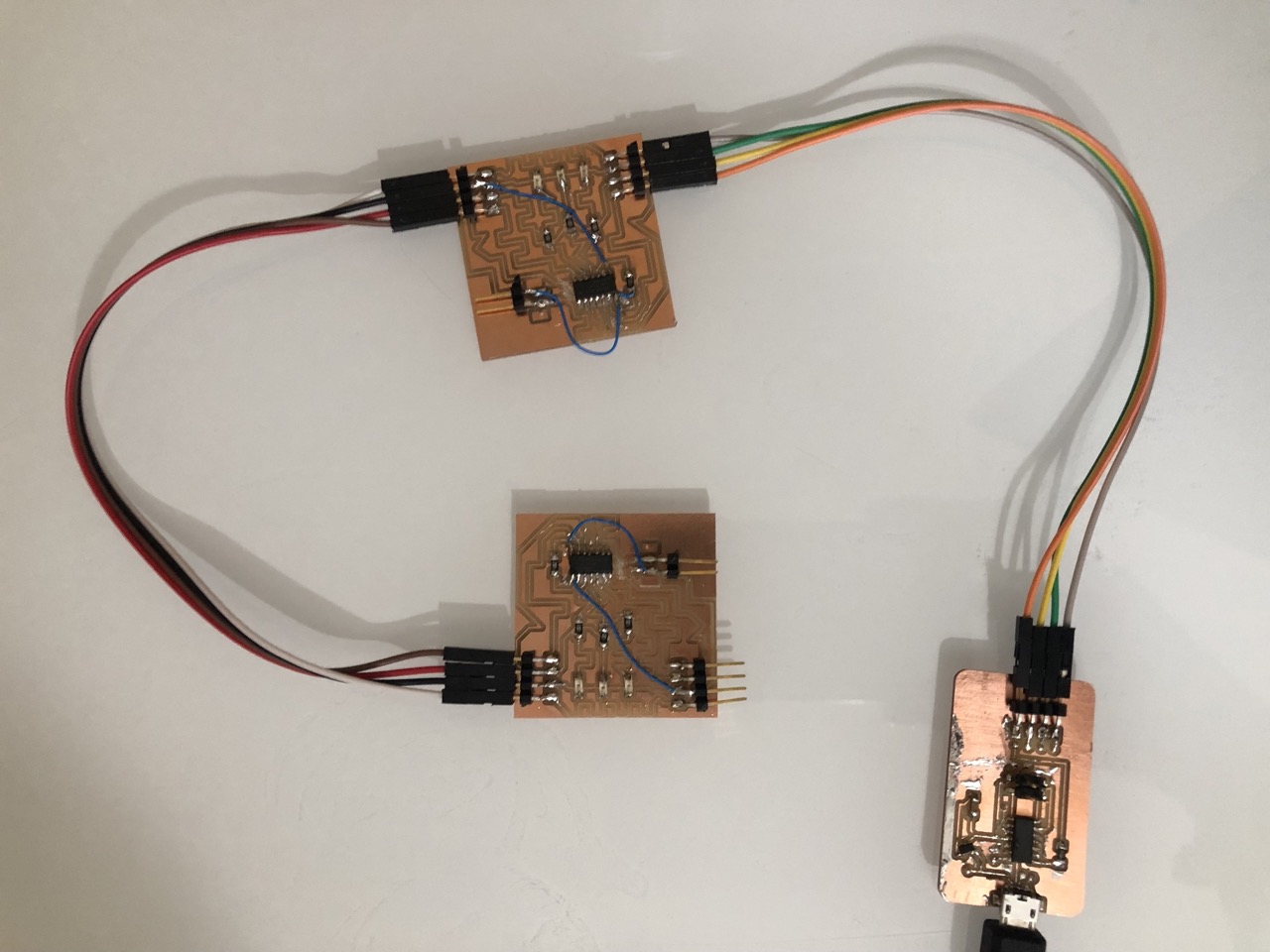
Connection across the three PCBs (after undergoing board surgery with jumper wires for both of board2)