Why do we need the components that we need?
I started with watching the ECAD design demo, and I was puzzled with why we need connectors in addition to the micro-controller. I asked Alec from EDS these questions and got some answers
- Why use capacitors? Mostly as buffer to filter out the AC noises.
- Why use regulators? To power down the voltage from 5V to 3.3V.
- How does the supply in Fusion works? Each 5V and 3.3V are connect to the others of its kind. The symbol just help to simplify the visualization.
- How does grounding works exactly? In a building, it is with metal stakes to the ground. In my computer and any USB connected to it, it is the negative side of my battery.
Side notes: There were a few days in which the EECS Labs wifi used in EDS did not work for me. I embarked on a long journey of figuring out why that is--including restarting my computer no less than three times and three separates trips to EDS at various time of day. I asked Dave and Alec from EDS as well as Adam from the EDS neighborhood. Then, I asked Anthony, who led me on a field trip down to the third floor of 38 then the forth floor of 36 to some interesting offices with marble heads and large maps of San Francisco and folks who never seen my problem before. The problem was eventually resolved, but I still don't fully understand what went wrong and what fixed it. This issue ate up a good amount of time before it was resolved.
Schematic Shenanigans
I first created the schematic below following the ECAD design demo but changing the board to a XIAO RP 2040. This design features a USB plug, a connector, a button, and a regulator.
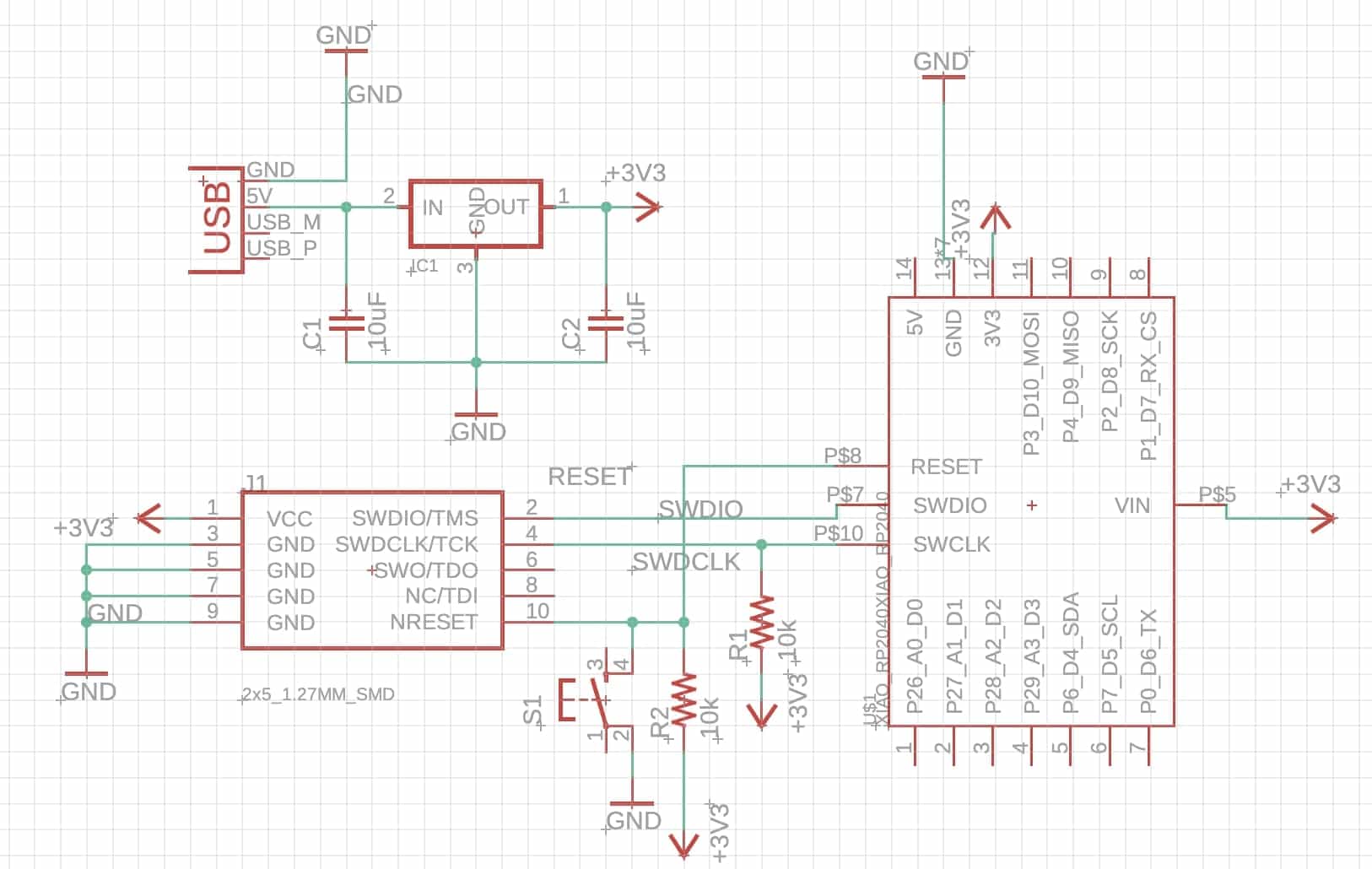
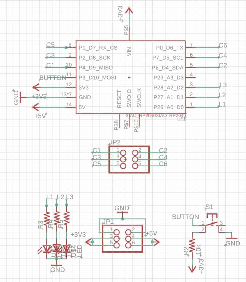
Then, I consulted Anthony who explained that many of the components I put in was not needed--mainly the adding USB (because the XIAO comes with a USB-C port) and the type of connector I was using. Specifically, the connector was more complex than the kind that I needed, so I change it to a more simple one that only connects to 3.3V, 5V, and ground. Since I dropped the USB plug and the XIAO has already take care of changing the voltage from 5V to 3V3, I also drop the regulator. I keep the button and added some external LED lights for funsies. The exact pins location of the XIAO on the schematics does not match up with the pins location in its documentation, so I shimmy them around a little during routing. What you are seeing below is the connections after I have shimmy them around.
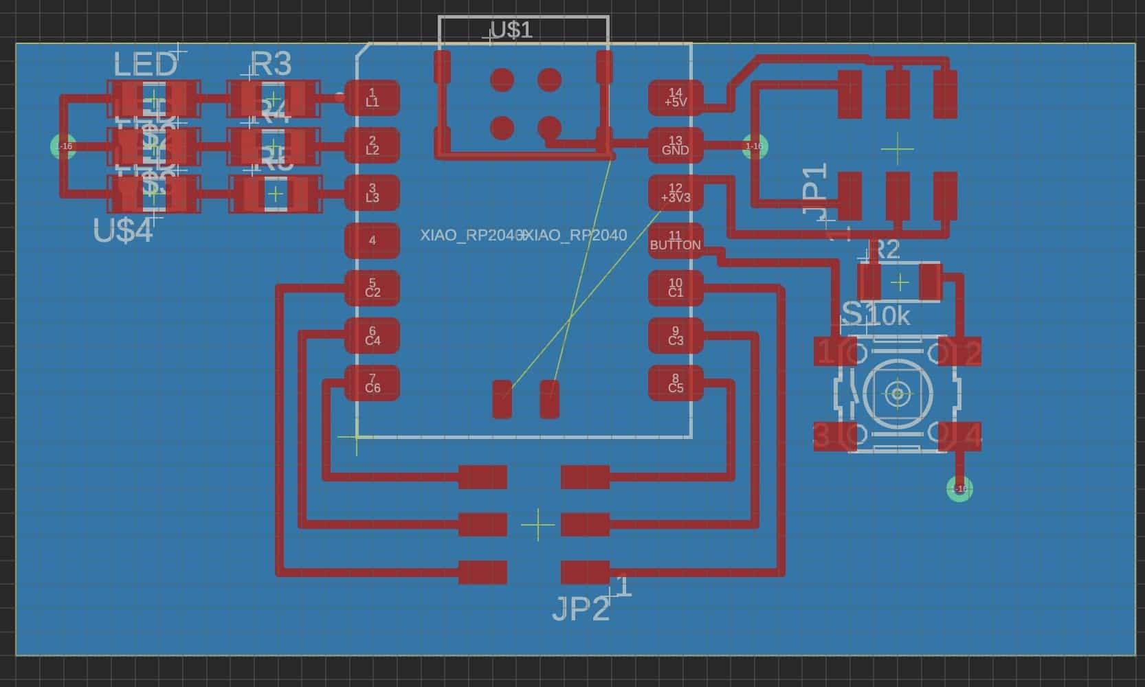
Routing
I naively started routing with 6 mil width which I have to change to 16 mil later on. I shimmied around and around until a find a good fit and then shimmied around and around some more for a better fit. Routing is quite relaxing--much like soldering! I placed some vias around to connect to ground, but, just like the route line, I started with the wrong size (1/32 mils I believe) and then change to the right one after (1/16 mils).
I learned that I do not need to route the two pins on the bottom (for reset and boot) to power nor ground because they are internally connected within the chip.
(Why are so much of the fabrication we have done is in IMPERIAL UNITS!??? This is such a terrible system. Wouldn't millimeter or micrometer be much better than mil? Why is a mil a thousandth of an inch instead of, say, a million? The odd conversions of the imperial system is much harder to do than that of the metric system, yet we are sticking with it <'_'<) Anyway, below you can see a picture of my final routing which I will mill next week!
You can find my schematic file here.