Final Project
Summary:
Overall, I learned a lot from the class. I got exactly what I wanted from it: an intro into everything. I hyper-indexed on learning the things I was the worst at: electronics and electronic design. Ultimately, my project didn't make it as far as I wanted because the key feature I wanted (the screen) didn't work.
So here is my Final Project!
Modeling - CAD
From our Week 4 - 3D printing week, we had a base model. However, we wanted to iterate on it a little more. Something with more curves and dimensions.
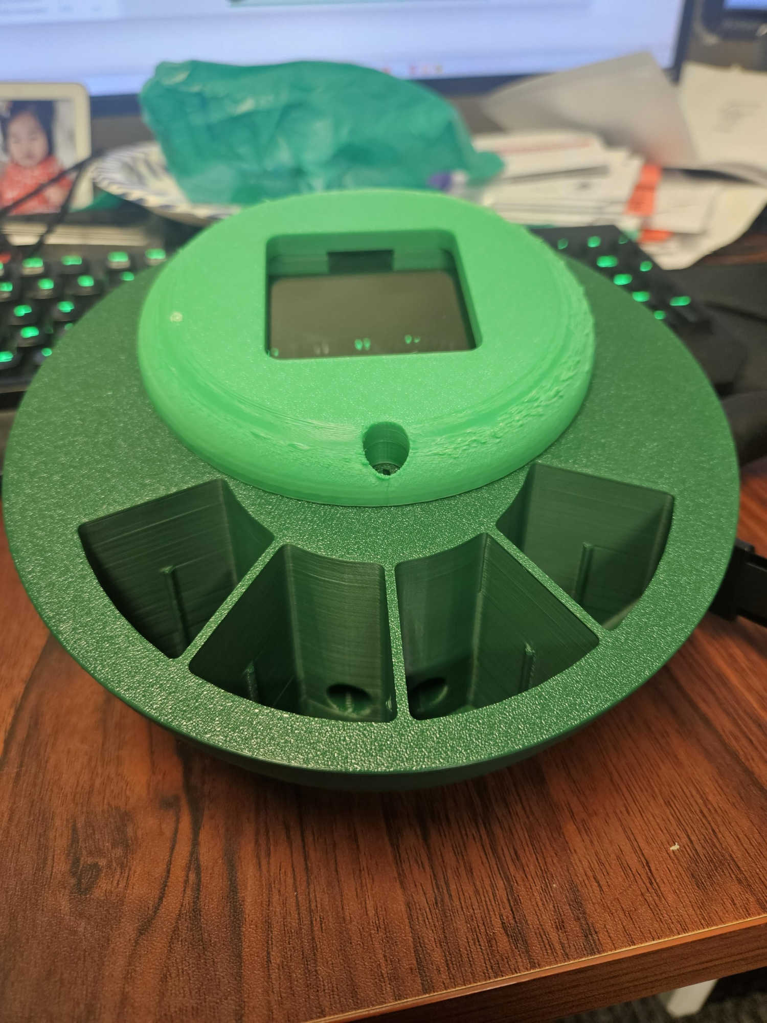
Our base served as good first iteration. It let us test a general shape.
A few lessons learned:
- We wanted an overall smaller build. This was too bulky as is (~500g in PLA alone)
- More curves!
- Only 3 buttons.
Note: Green was only a test print (as it was already loaded into our printer).
So, we started all over in Solidworks:
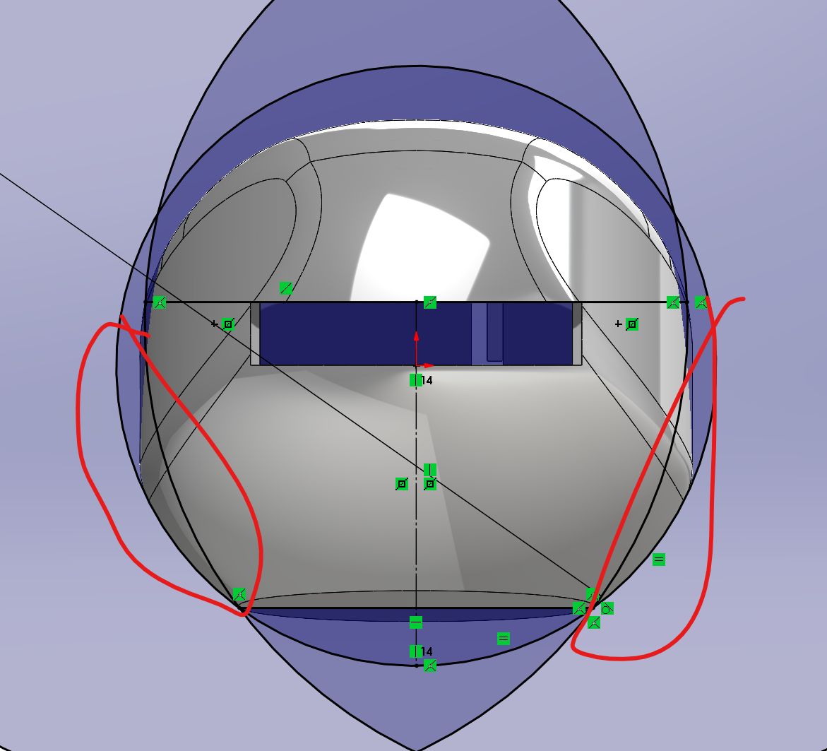
Halfway through iteration - building speaker grill/mount
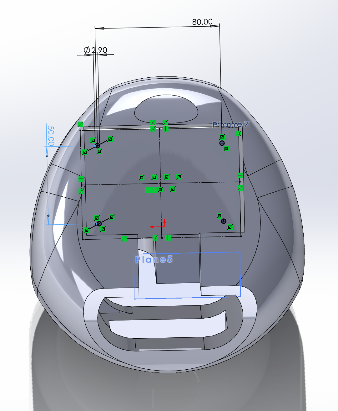
Our PCB mounting directions M3 screws in an 80x50mm grid pattern. Everything will have to mimic this.
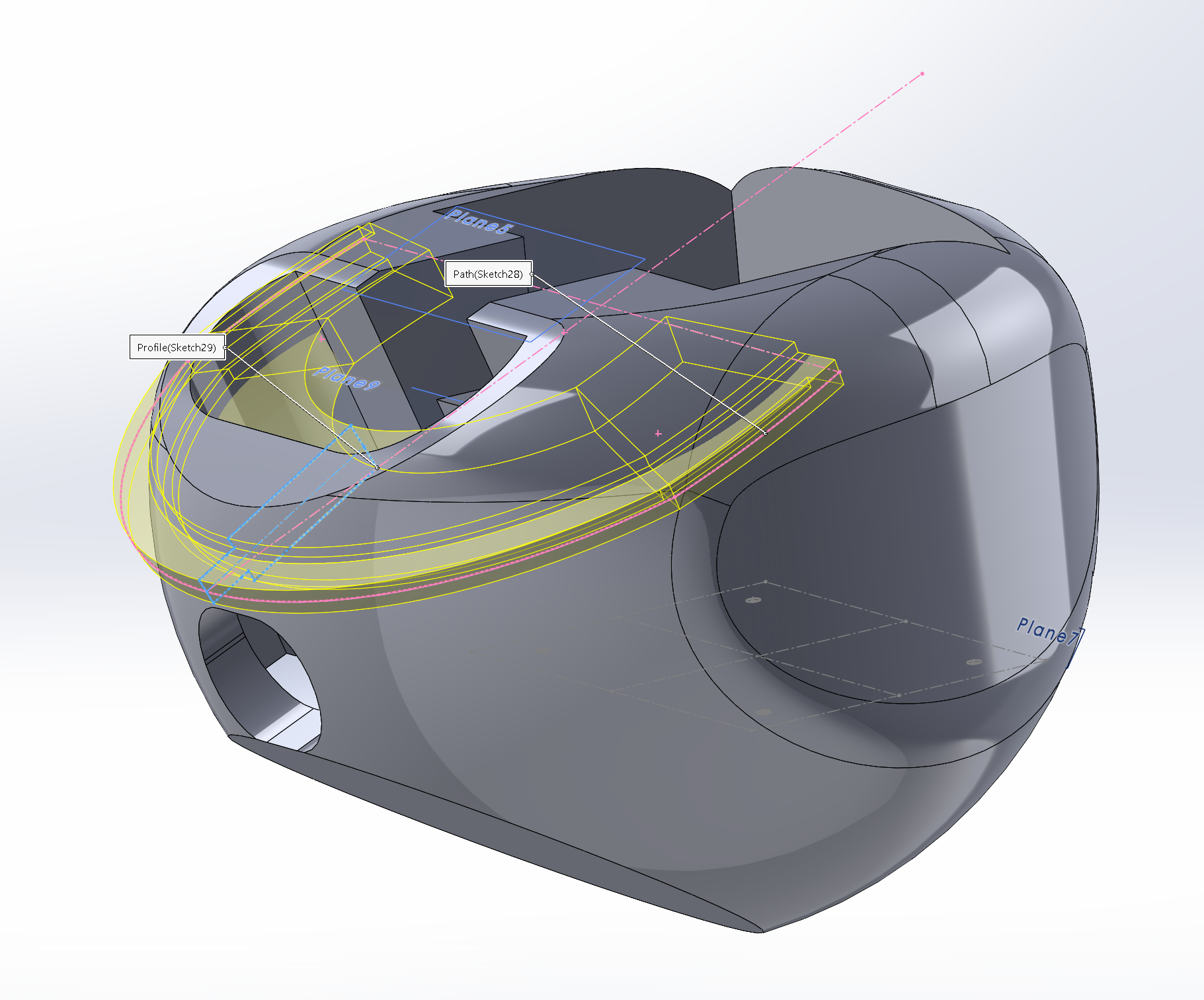
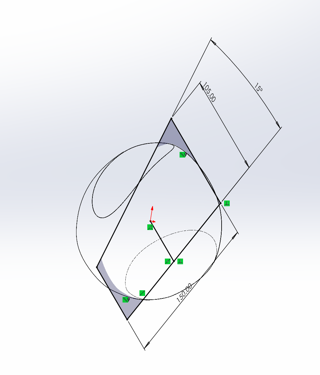
The hardest part to CAD - the wrap around LED strip. The only thing harder is going to be the covering we're adding to the project.
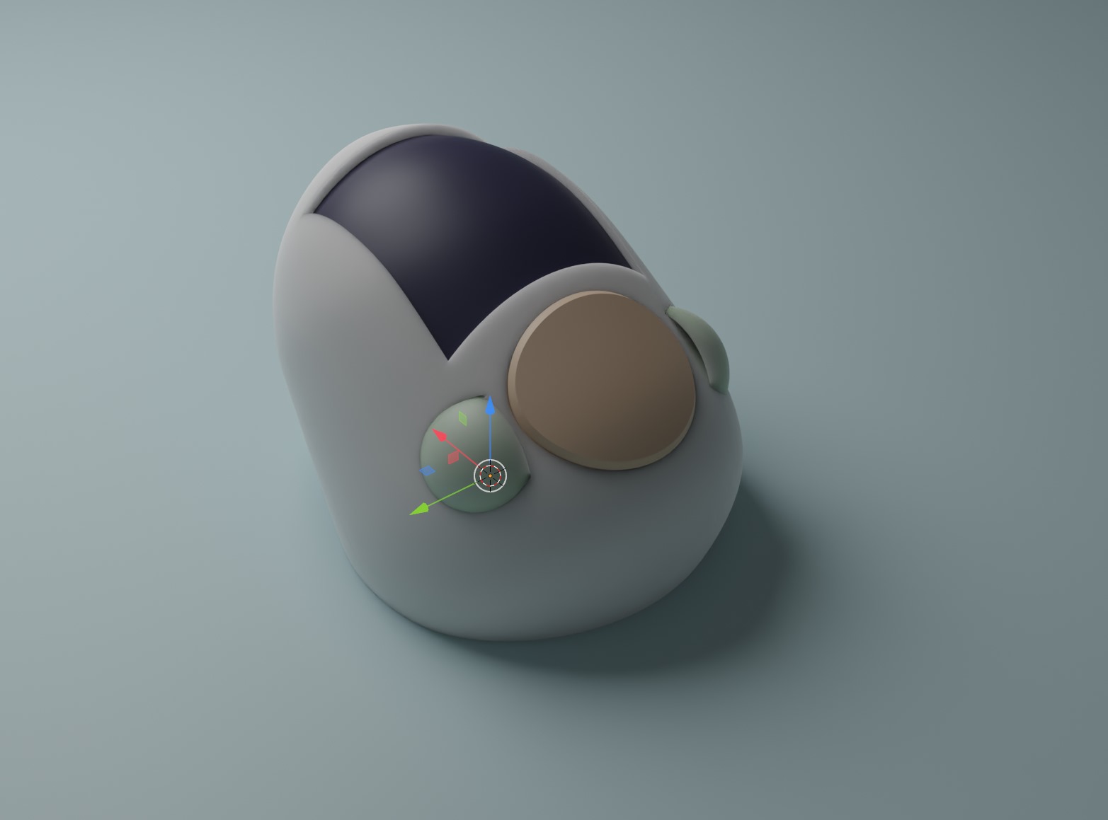
Body Iteration 2
Lessons learned from initial prototype:
- Needed to shave a ton of weight. Overall goal is to reduce the size of this substantially and weight of this. Even without the battery, the weight of this device is to the point where if you drop it, it would hurt a child.
- I need more mounting points for the multiple boards.
- Speaker looks too exposed.
After the first print, I want to make the egg skinnier. Here we are cutting away some of the profile
Additionally, we made a few more changes:
- Added a support to the screen.
- Made the button area larger.
- Added a speaker grill.
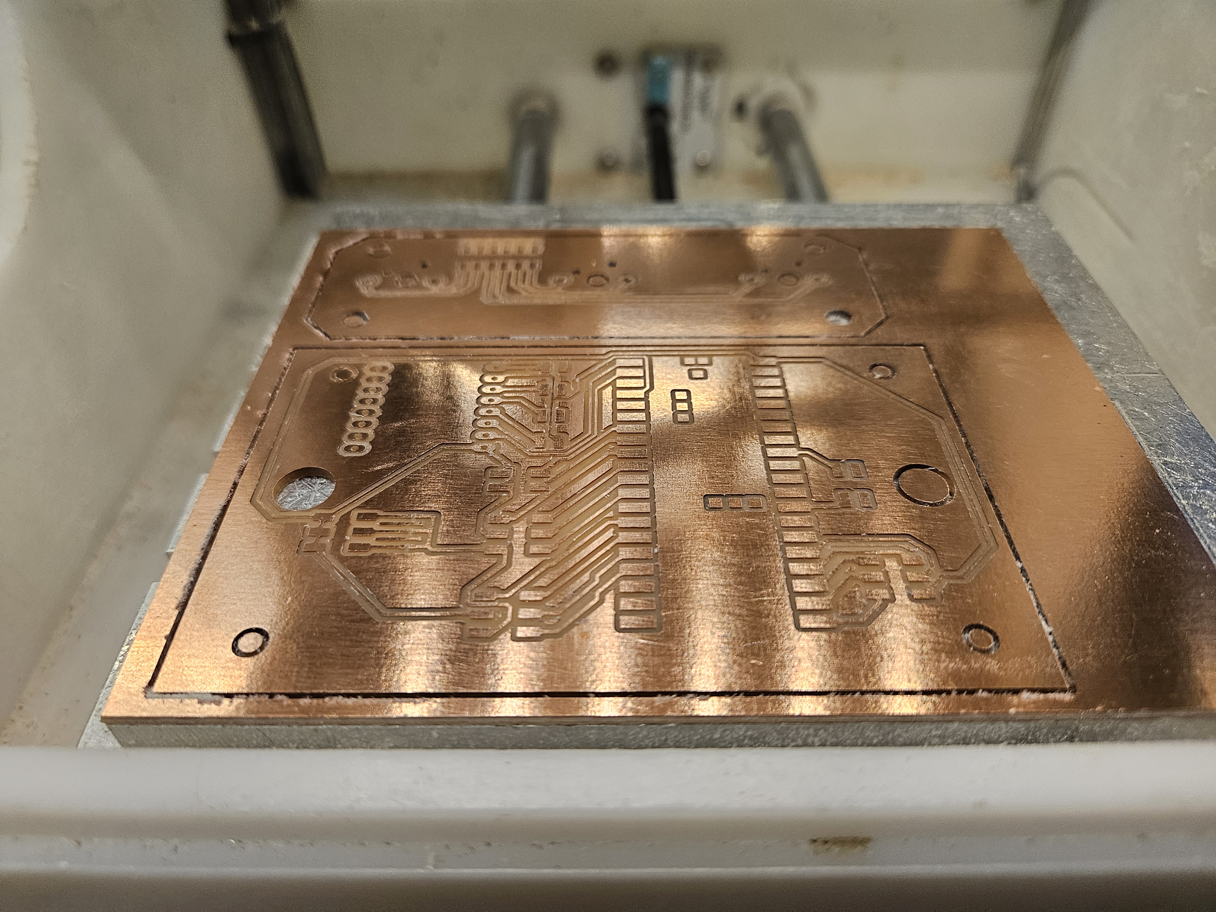
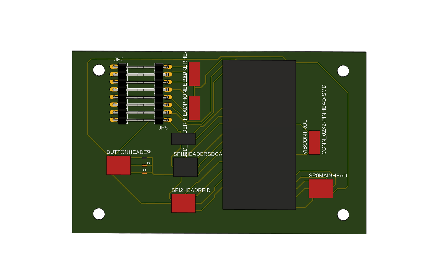
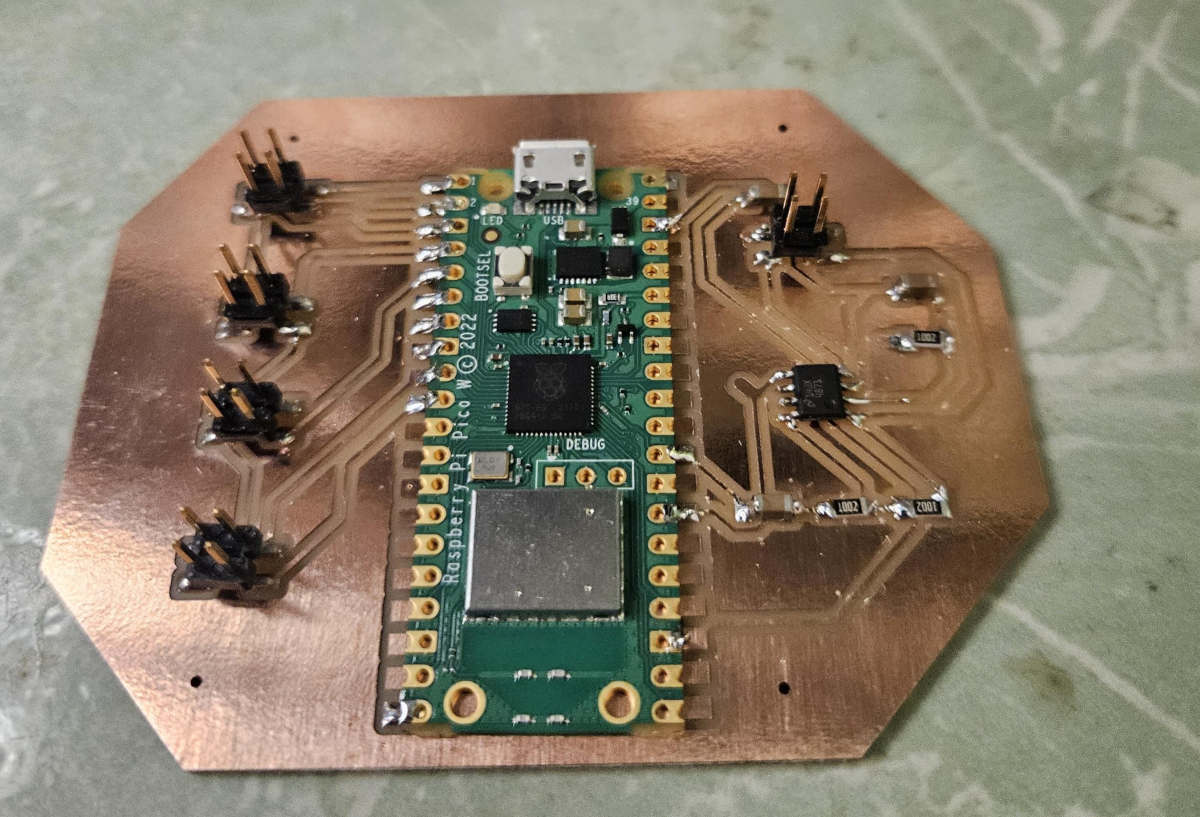
Electronics Design - PCB Main
We have iterated this multiple times over the entire course (since week 3). A few iterations can be seen in our log.
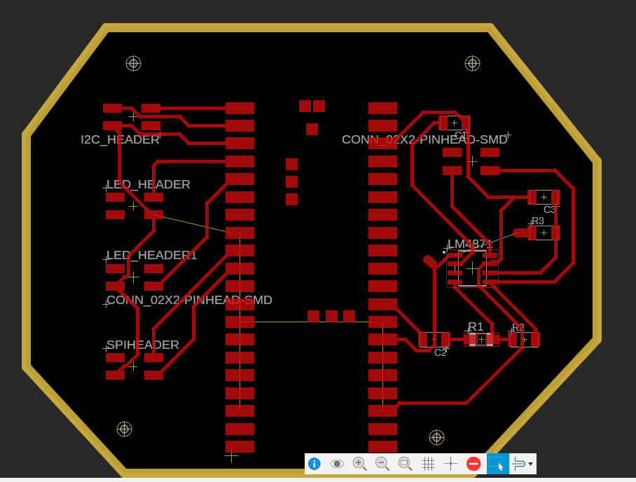
This wound up being our final design:
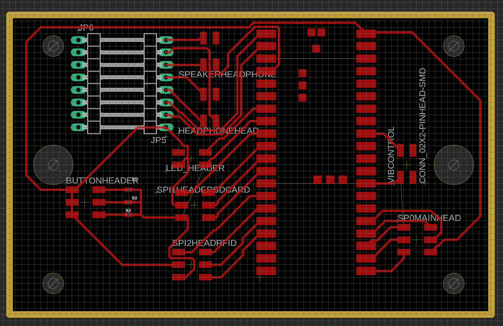
As you can see, we generally got A LOT better in being organized and "tighter" on our board. Still, a lot of room to improve, but we are definitely seeing progress.
A few key design notes:
- Still used the RP2040 Chip (switched from ESP32 @ Week 5)
- Went from directly mounting circuits to mostly wiring headers
- This allowed us to focus on software mostly
- Allowed us to include more and more modules
- Wound up being significantly worse on space in the module
- The smaller mounting holes on the side are designed as direct mounts.
- The larger holes on the side (East/West sides) were actually placed in order to create the inner structure to support the other 3 boards.
Mistakes - the header for the switches became significantly more complicated than it needed to be. Eventually, the switches were just directly soldered onto the chip GPIO slots.
Now that we kind of have an idea of what our electronics we need to do.
We quickly pulled some open source files for our PN532 board and RA8875 boards. We then pushed these models with our CAD spitout from Fusion to a Solidworks Assembly (almost entirely because its easier workflow on my end).
This lets us take a glimpse of version 2.
Mounting Holes:
- 2x M2.5 Screws
- 5x M4 Screws
- 10x M3 Screws
Electronic Design - PCB Switch Board
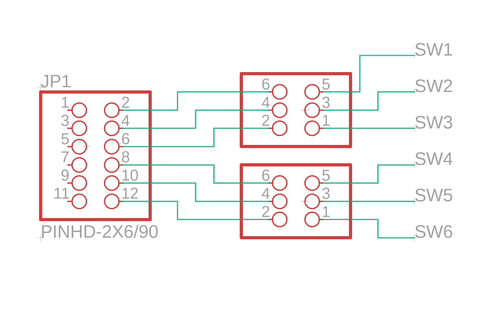
This is our switch diagram. Very simple. The more complex part is below where we need to make sure our dimensions are correct for our keyboard switches.
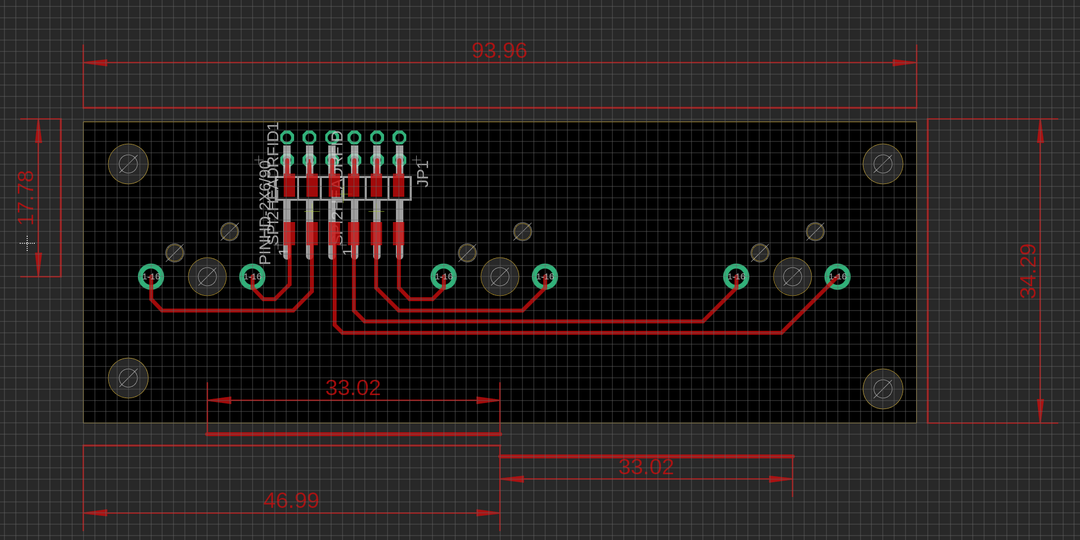
Very simple PCB with the layout made for Keychron footprint. 4 holes in the corners for mounting. Unfortunately, I was unable to source the parts for a through-hole header to mount the headers to. Instead, we went with normal headers for our final project.
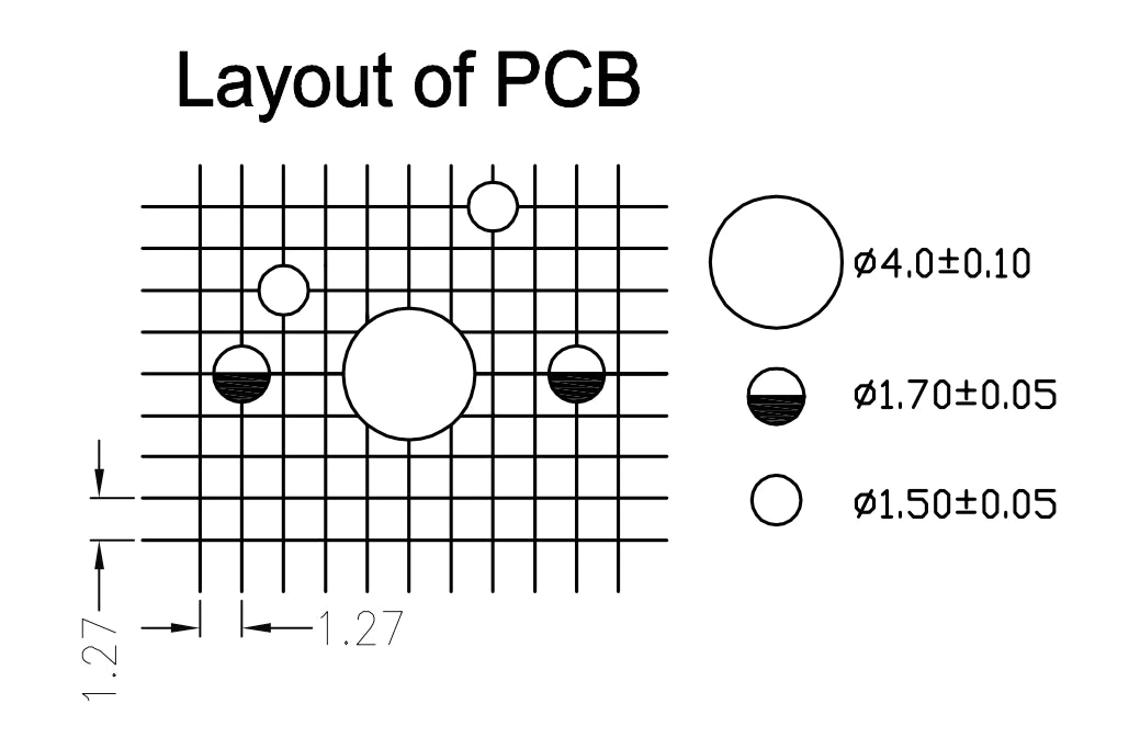
We used this image in order to get basic measurements for our push-button PCB. This was a great starting point but required slight modification as we messed up our contact hole and structural hole. Additionally, the support hole was slightly too far out. Measure once, cut twice...
We then reorganized our board, soldered out connections and tested circuits.
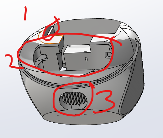
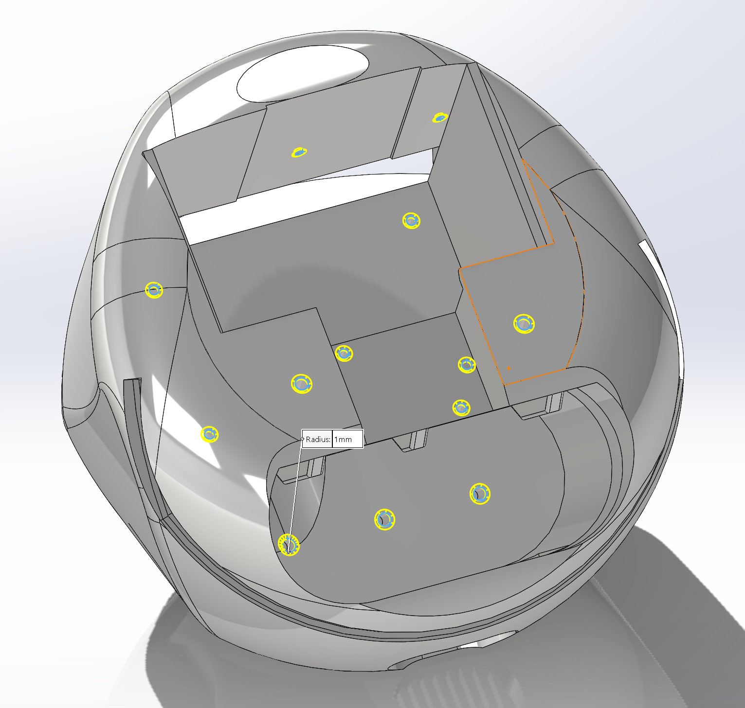
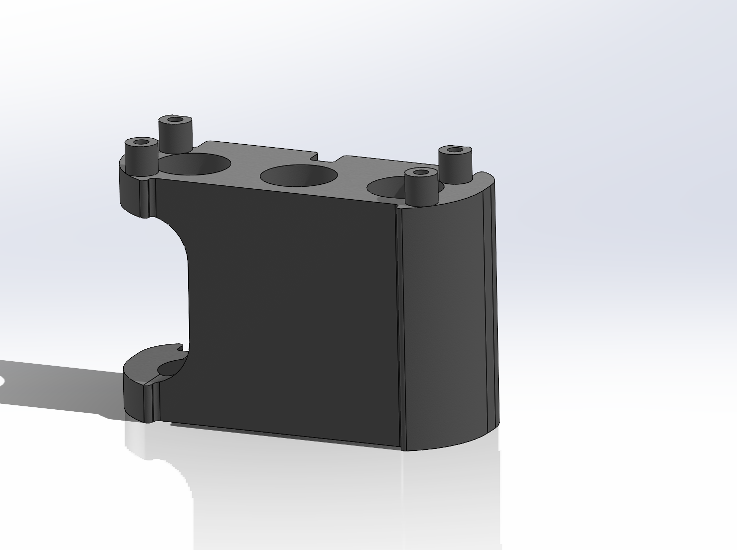
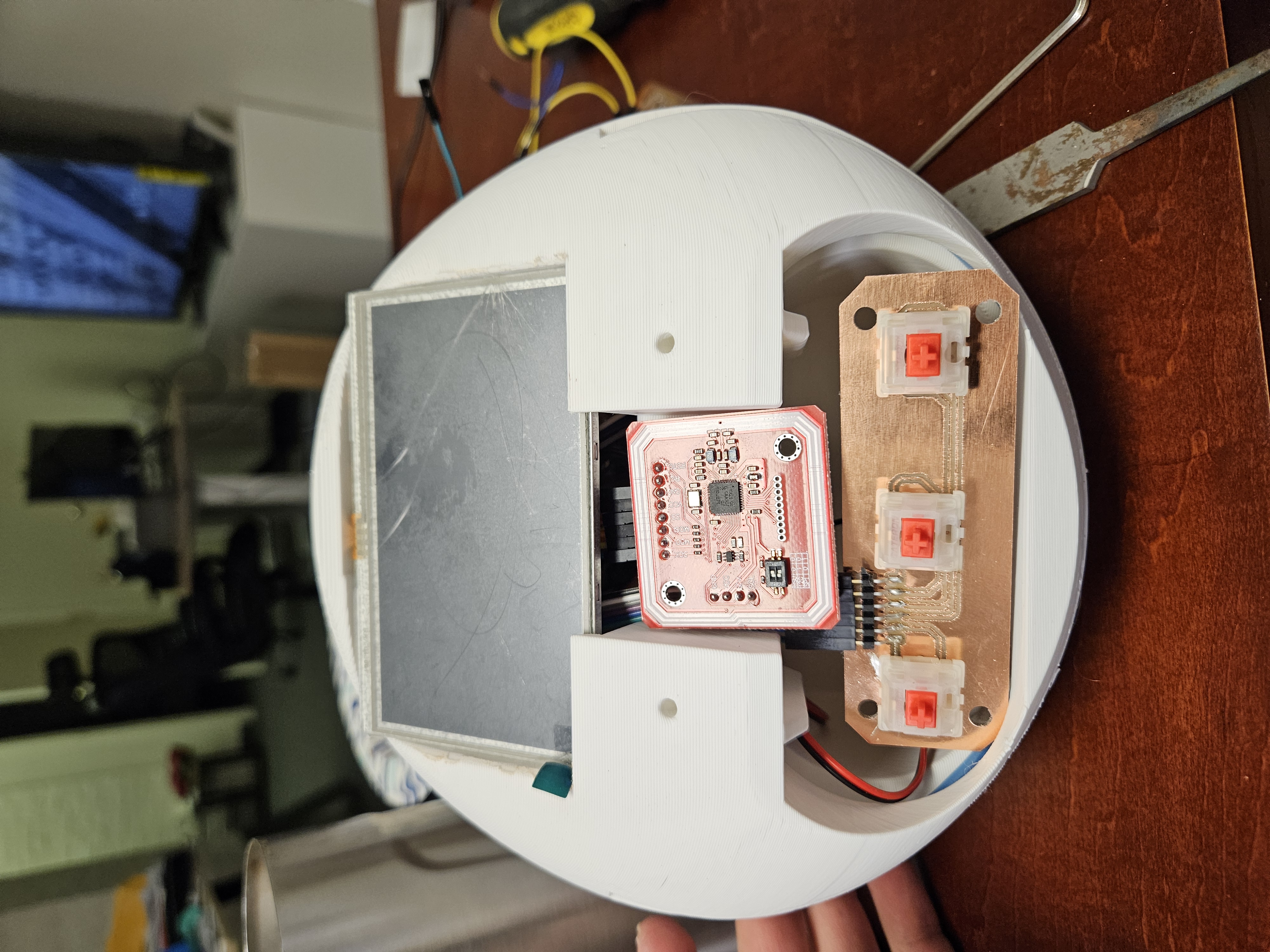
Internal Structure
For this project, there are quite a few different structures that we need to create in order to support our multiple boards.
Firstly, the support for our main PCB needs to be supported. We included a massive 8mm hole in order to allow us to create a support structure on top of our existing board. This will also alleviate any issues for our device shorting out eventually.
Secondly, we need another support structure in order to get support our PCB for our buttons. Our button PCB will need to be both supported then able to support other devices.
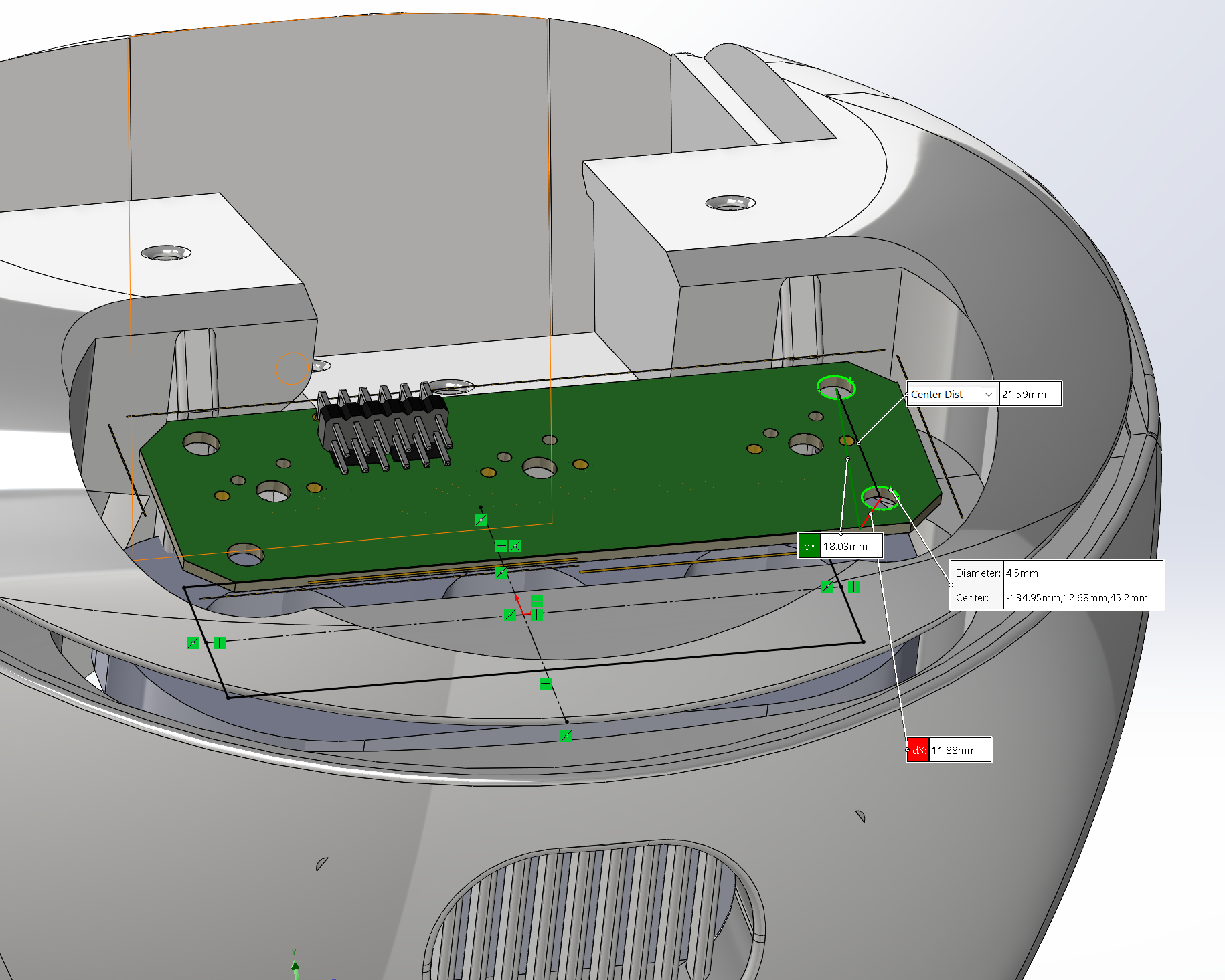
Third, we need another structure in order support our RFID chip reader (NF 532). This is the most critical as the distance between the surface and the board is critical for the device to read a good signal.
Finally, we need to create a block to support our display board (RA8875) chip. This was easily the most complicated because I accidentally soldered the headers incorrectly. This was a critical error because it caused us NOT to get good contact with the board and wiring. This became a bigger issue once we began designing the internal structure as it became extremely space constrained.
Button Design
Once we created our button PCB structure, we were able to create a button cap, trim, and internal spring to the design. We created "followers" or rails on our main body. This allows us to maintain the button dimensions while still getting good tactile feedback. For actual buttons, we are using keyboard style buttons. This poses some challenges.
Ultimately, we used rivets in order to place the backside of the solder. This allows us to keep the keycaps in their normal orientation. However, we didn't measure them and had to make the board twice for this application.
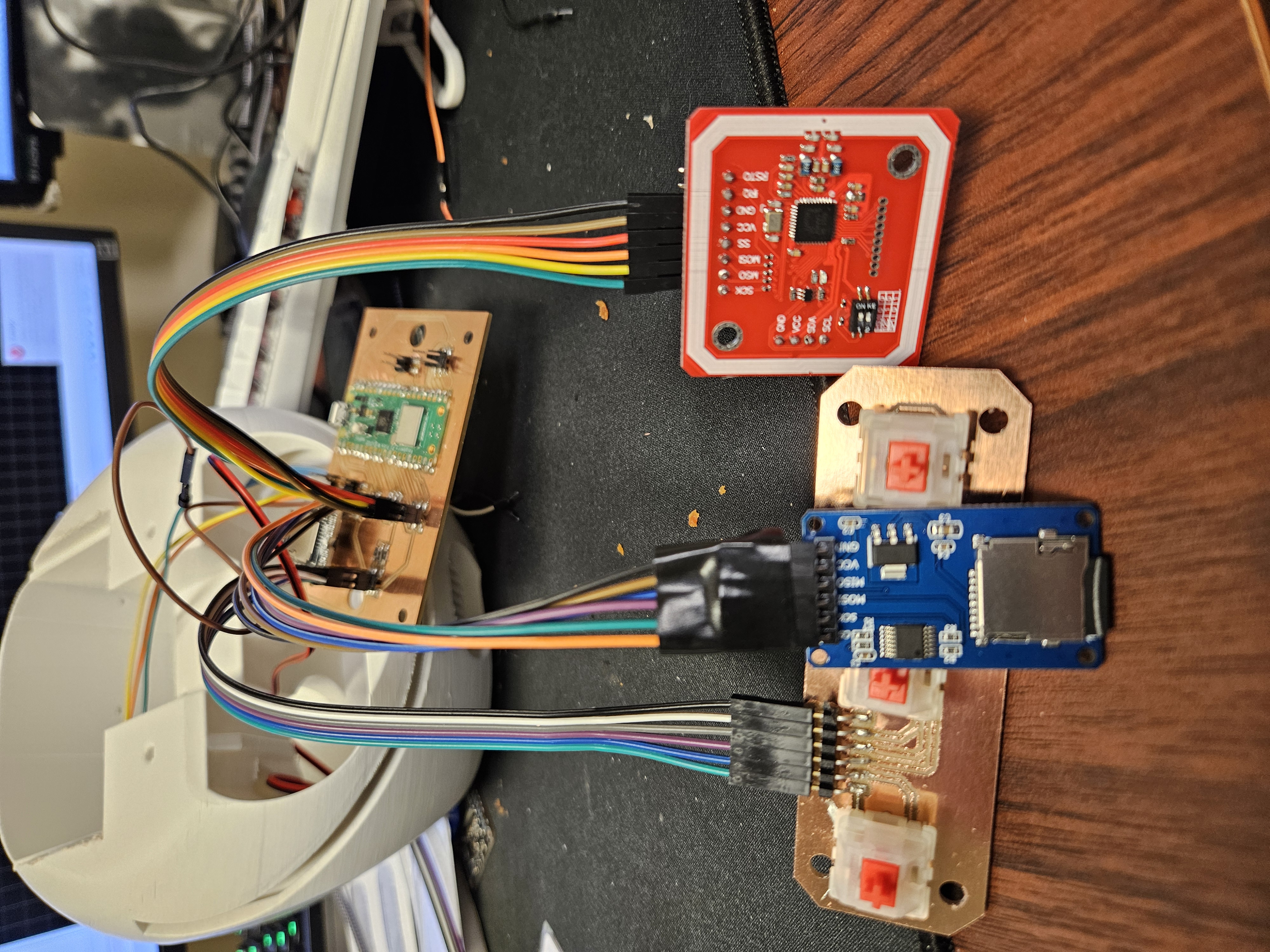
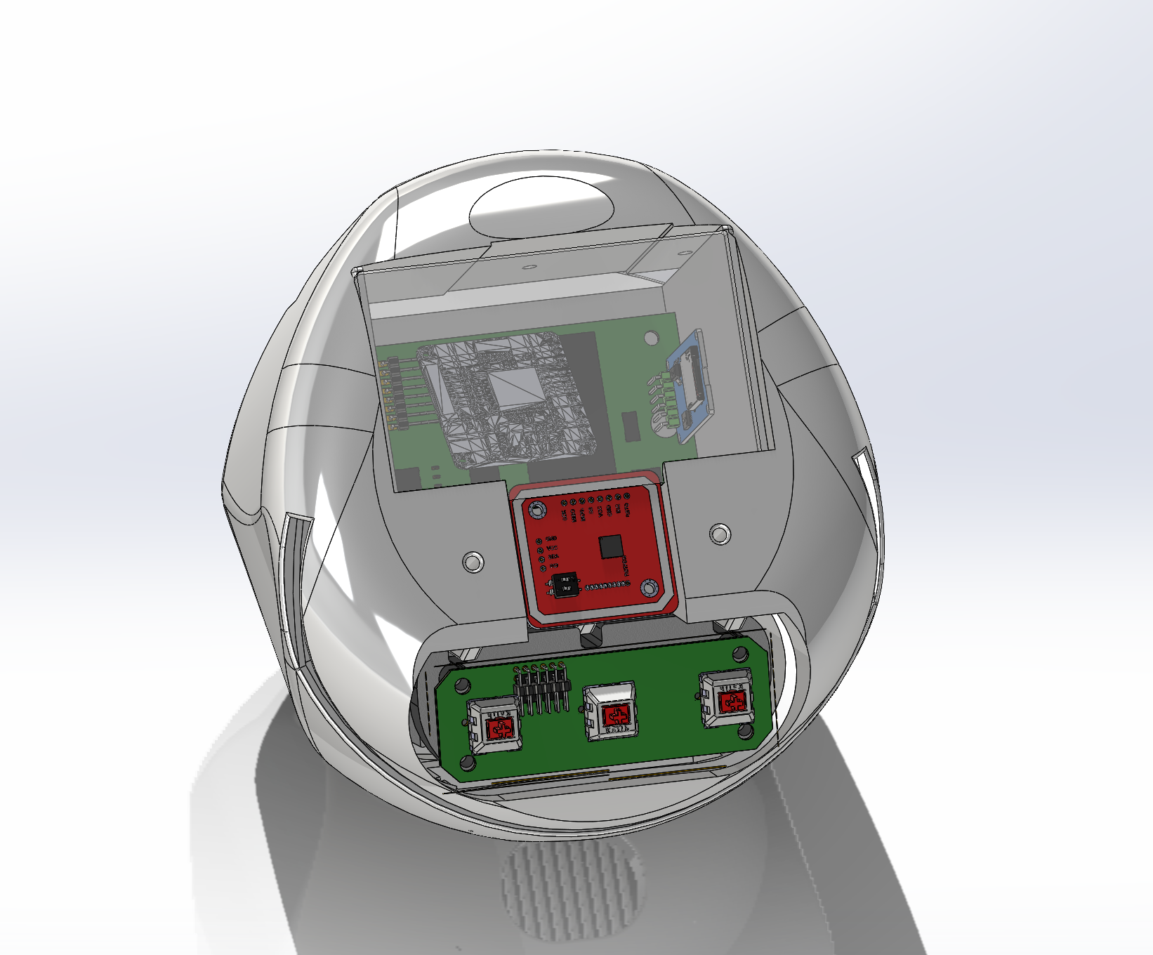
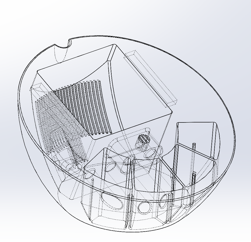
For our final design, we wound up with the following internals.
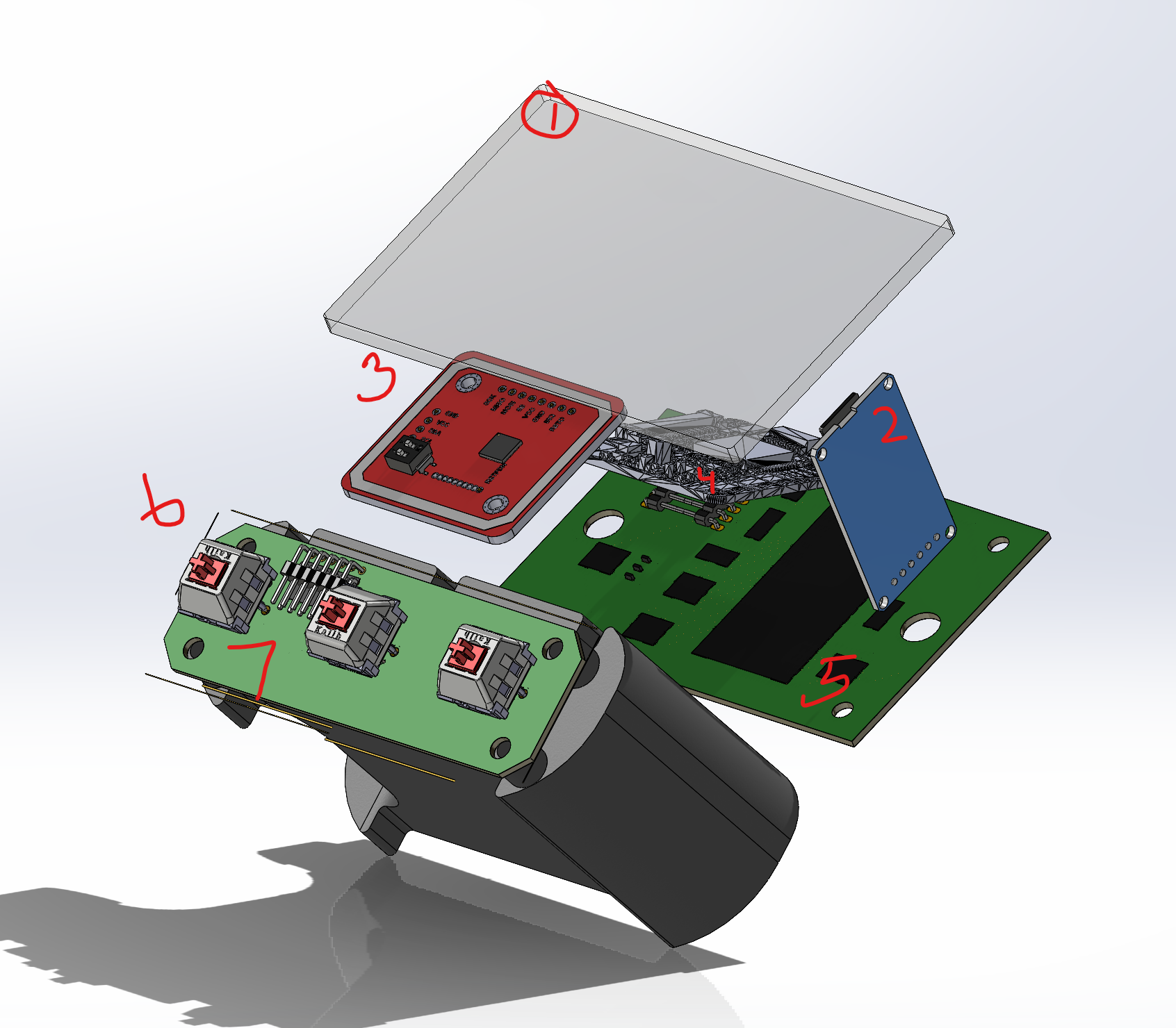
In order the following components are as follows:
- 480x272 pixel screen (4.3" in diagonal measurement)
- SD Card reader
- RN532 NFC Card Reader
- RA8852 Digital Display Output
- PCB - Mostly Wiring + DPRobot Mini Player
- Key Switches - Keychron Gateron Milky Red KS3
- PCB - Wiring and header for switch to main board interface.
Digital Assets: Voice Assets
TTS website to incorporate text to speech files in MP3 format for playback. We initially went with Azure TTS services but then opted for a free version. For The Korean version, we used a free website.
Korean: https://www.narakeet.com/languages/text-to-speech-korean/
English: Azure TTS module below:
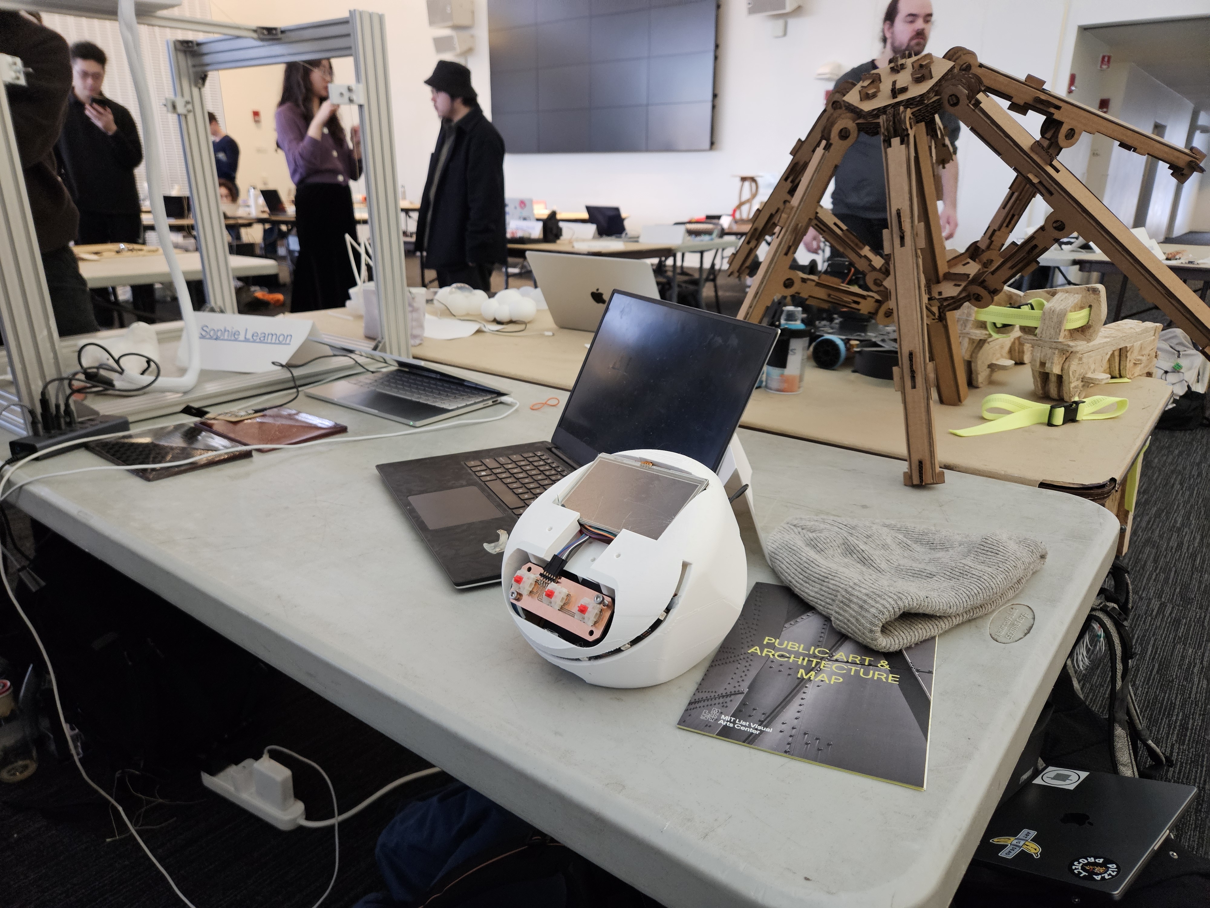
Final Assembly
We plugged and tested (and trouble shot - HEAVILY) our final project.
It was mostly just plugging in cables (in the correct orientation) and screwing down our boards.
We finally made some progress! Components were working... then...
Disaster
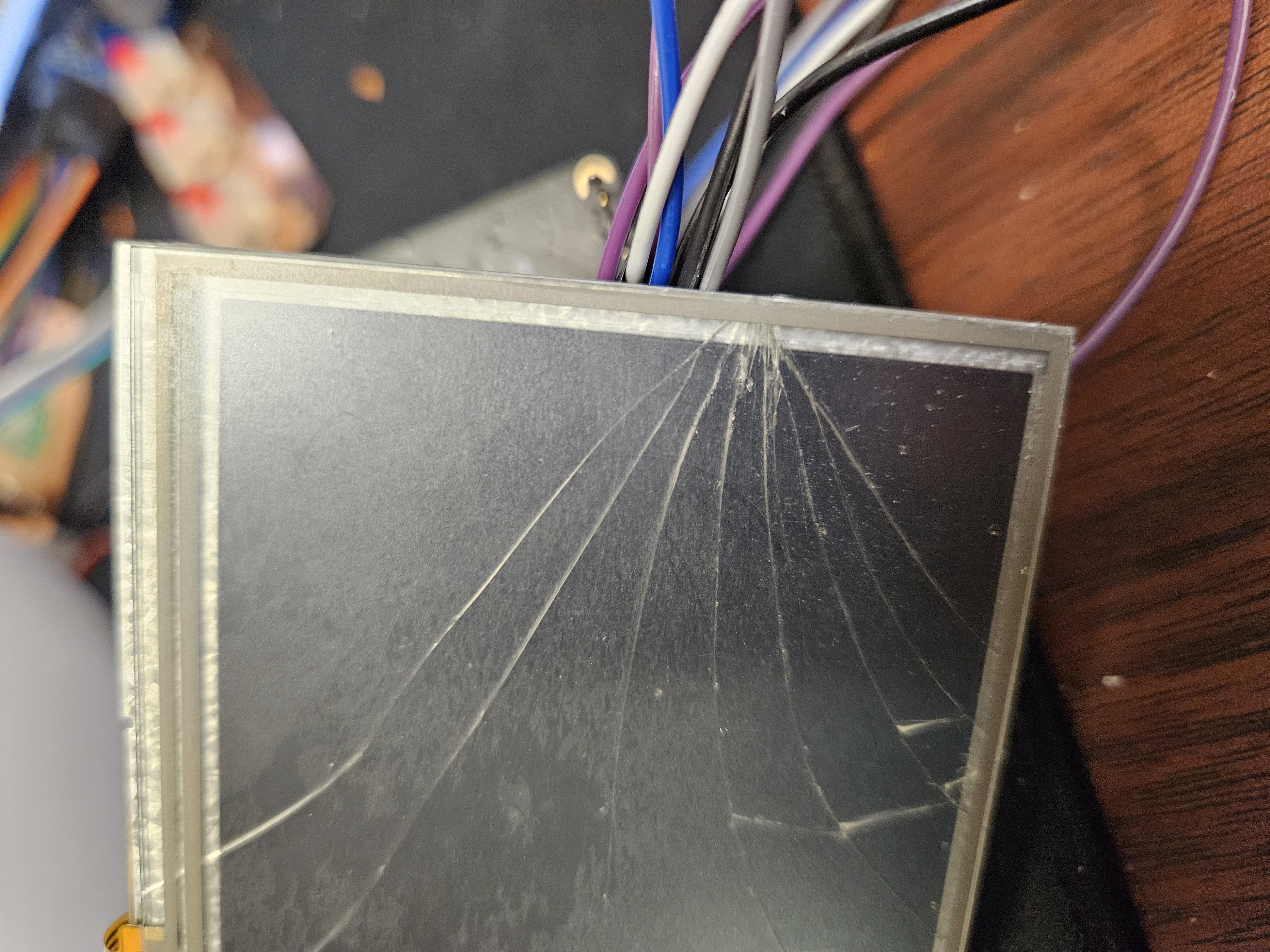
While pushing the screen into the device, our screen cracked. Unfortunately, I actually think the screen should be fine and that it was the capacitive touch screen that failed. However, our board was reading the RA8875 chip but it was not outputting a single image (or even turning it white).
So we moved onto completing what we could for our final device:
Digital Model:
Reality:
Final Project Video
Closing Thoughts
I ultimately had a lot of fun and learned a ton both from the staff, but more importantly, the other students. I would highly recommend taking the course if you have any intent on doing anything technical.
I invested some personal money into the project. This was almost entirely on the screen and screen driver. I acknowledged I didn't have the personal skills to build a driver board, driver software/library and time to create that aspect. I also wanted to make something my daughter could immediately play with. Unfortunately, I did not get to hit some key elements but we did get audio and lights working which were key features on the project.
You get out of this class what you put into the class. A lot of time, a lot of work but extremely rewarding.
Final BOM
- Hardware
- PLA - ~260g External; 140g internal (~$10)
- Connectors (<$1 Total)
- 2x M2.5 Screws
- 5x M4 Screws
- 10x M3 Screws
- Misc Female x Female Resistors (x28)
- Electrical Tape Misc
- Electronics
- 7x WS2812 LEDs (Roll of 250 LEDs $12.19)
- 1x Box Speaker (8ohm) (~$5.64)
- 1x Adafruit RA8875 Driver Board ($29.98)
- 1x Adafruit 480x272px display (4.3" in) ($27.42)
- 1x PN532 NFC Tag Reader ($8.99)
- 1x SDCard Reader ($4.89)
- PCB Construction:
- 1x FR-1 Circuit Board Stock (This will be split into two)
- 6x 2x2 headers
- 3x 3x2 headers
- 1x 1x6 90-degree header
- 3x 233K Ohm Resistor (1206SMD)
- 1x DFRobot Mini Player ($5.99)
Overall Cost - $106.01
Tools
- Software:
- Fusion 360 - almost exclusively for EDA
- Solidworks - CAD
- VSCode - IDE (Arduino)
- Hardware
- 3D Printers
- Bambu X1C
- Bambu P1S
- Prusa MKS3+
- Drill (Tap Holes)
- Soldering Iron
- Other Machine Co (OMC) CNC Mill - NKA - Bantam Tools
Final Project Logs
Lessons Learned - Mistake Log
- Measure once, cut twice - went off a diagram online instead of psychically measuring keycaps.
- Measure once, print twice - used too small of a measurement for the screen. Screen didn't fit in the first mockup.
- Soldered Headers backwards.
- CRACKED THE SCREEN!!!
- Reversed UART pins for RX/TX
- Admittedly for the RP2040 Pico, RX and TX are reversed for the SPI and UART
- ^ WHO MAKES BOARDS LIKE THIS?!? ^
- Completely didn't complete the ground wire on half of my board
- Shorted #2 Switch (middle button)
- Used the wrong footprint for the Resistors (PITA to solder)
- Missed clearances on the header pin. The header fits, but the wires that attach to the headers don't.
- Completely missed soldering on a pin on the header (5 out of 6 pins were soldered)
Previous Weekly Updates on Projects
This page will track the status of the final project as we go through.
This will also serve to cover the first class assignment involving CAD
Project Summary
Build a device that can teach my daughter to seperate vocabulary from different languages
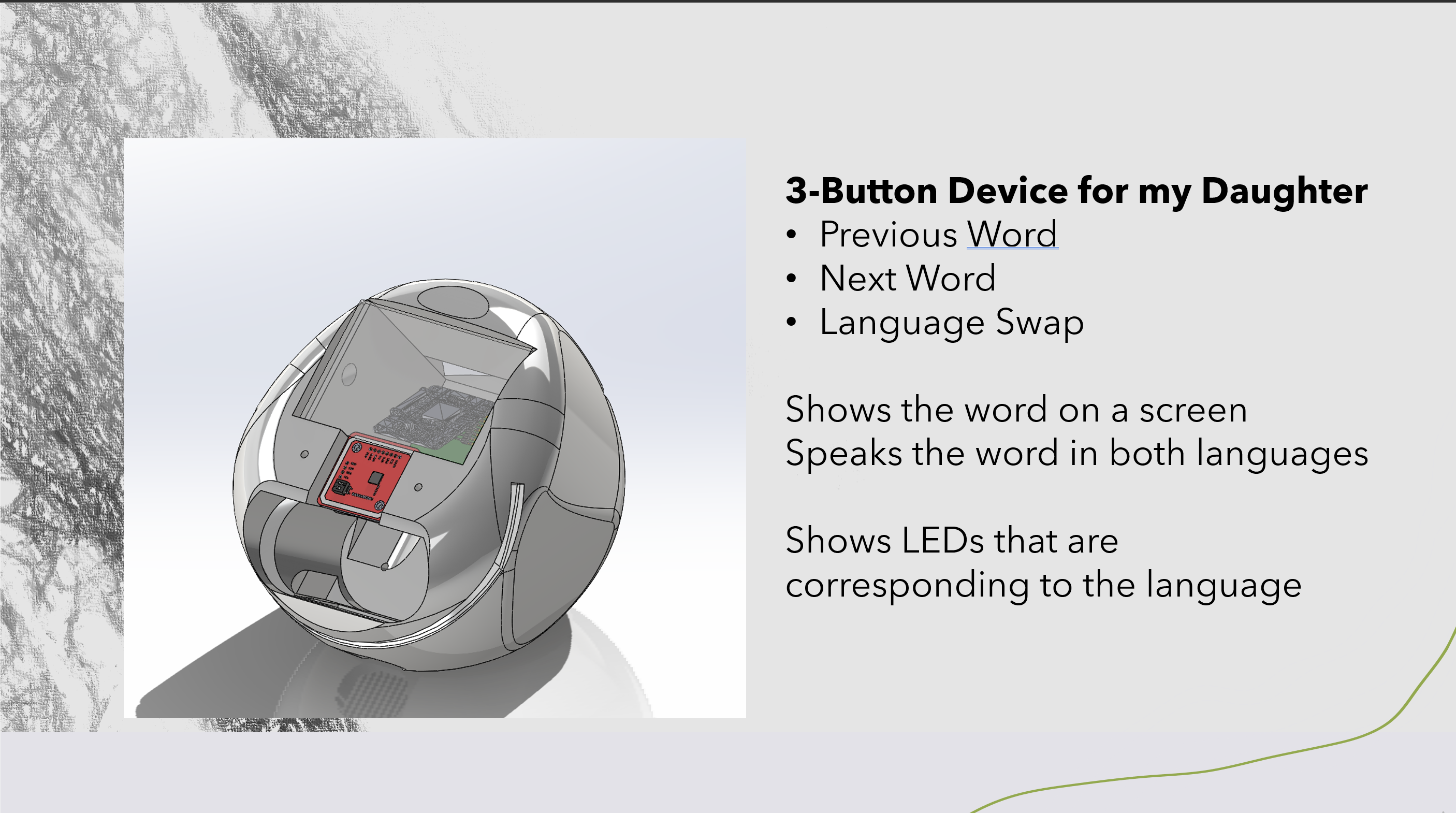
Concept Design
Problem: my daughter (2yo) grows up in a bilingual househould.
When she learns vocabulary, she does not know if the vocabulary she is learning is from Korean or English. Instead, she knows that there is the possibility that two words can mean the same thing. hink like head vs hair - they generally point to the same area. However, for different languages, she is not able to compartamentalize different words. This means that she has trouble understanding which words she needs to use when she talks to different people.
Project solution: Build a device that can use lights, sound, vibration, etc, to teach her vocabulary while segregating them into different cues. I.e. a blue light will bounce when an english word is presented, a red light will bounce when a Korean word is presented.

The first assignment was a concept sketch of what you wanted to build. This was a quick CAD of roughly what I wanted to do. Its basically a table that can fit multiple buttons. The center console will be a screen that can project words.

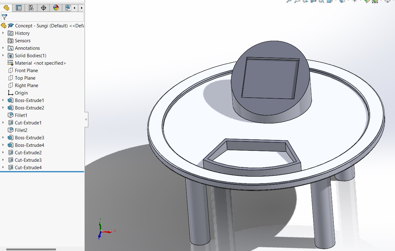
The concept is to take a word in English, align it with a picture. Upon toddler input--a button in this case--show that word in the opposite language, this being Korean. We then associate that word and language with a corresponding color. We will be using blue and red as the colors for English and Korean respectively
After the first concept iteration, we realize that the project may be more manageable from a physical inventory standpoint if we just make it the interface. Additionally, we found that we will utilize some of the material concepts in the class to build this.
Update - Week 3
This week, we solidified our design. Our desgn was inspired off an "egg". We took an egg, sliced it on a bias, then created a screen and button interface.
We changed a few things this week
- Final Project will no longer include the table/stand
- Four-button interface determined
- Screen is around 3in x 3in - note, if we get a screen, this design may change completely. The screen size is NOT parametric design so this may be alot of work....
- We designed a removable, magnetic lid, mostly as a convenience for the design. This will allow us to access and plan the inside without much issue, given how easy it is to remove
- Lid may be completely redesigned in order to have a more "egg" feel to it
- Protype colors are not relevant; still deciding on color scheme - note, white is the favorite for the "egg" theme

Update - Week 4
Made some edits to the code
We added some modifiers to play Mario
Will insert compressed Mario video here:
Update - Week 6
Created a base for the board
 Note: there are alot of issues already
- No headers for buttons
- Only setup for mono speakers
- Will most likely require multiple individually controlled LEDs strips
- Separate board - for space issues.
Update - Week 7
Created buttons for the design - however, I ultimately decided that I dont want to my daughter slapping stone buttons. This will ultimately be plastic - probably ABS.
Update - Week 9
We coded the ambient light sensor. We validated a few things that we need for the screen: 1. Our phototransistor needs tweaking either through an additional resistor or a different transisotr all together. 2. It is very sensitive to light angles so it must be direct. We can solve this through being intentional of our geometry and placement.
Update - Week 11/12
We worked on the screen. After realizing that we needed a bigger screen, I looked at ways to get a bigger screen. I looked at ways to push pixels to larger screens. We decided on the RA8875 and corresponding driver from AdaFruit.
 We prototyped the board output using a breadboard
Current Remaining Feature Dev List
- Finalize Screen output
- Push words on screen
- Push images on screen
- Speaker - WAV/MP3 File output: Currently can push tones - need to do WAV file reading
- Redesign mounts for PCB
- Redesign button mounts
- Korean word text translation to video driver
"Nice to Have" Features
- Battery Operated
- RFID Reader
- QI Charger