Individual Assignment Prompt:
- make and test the development board that you designed to interact and communicate with an embedded microcontroller
Part 1: Revise Your Design Five Times
This week I had the personal goal of making something that will contribute to my final project's development. I had started this process in the previous week, and while that week helped me arrive at a scheme that could push the final project forward, I hadn't yet resolved all the details. So this week started with many, many questions.
Hopefully you're able to begin this week having most the design already sorted out, because you will inevitably need to make accommodations to match your footprint library to whatever the available stock is in your section, and do a bit of value engineering.
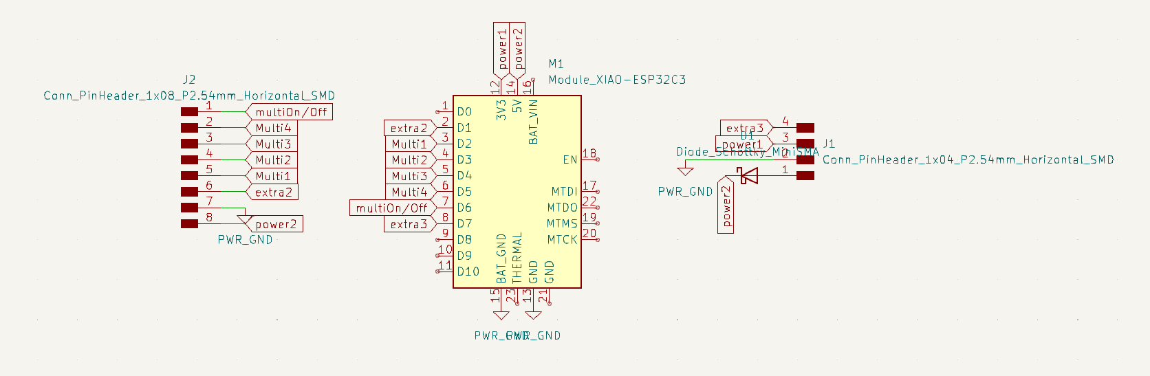
Okay, let's start with some vocabulary I didn't end up picking up until the end of the week. There is a difference between "development board", which contains your microcontroller and 'breaks out' it's pins, and "breakout board" which is an additional PCB that you're planning to somehow attach to your development board. I was confused because I had heard "breakout" as a verb being used to describe attaching your microcontroller's pins to traces on your PCB, making them available to a larger circuit. This schematic is of my development board. As shown in the previous week, I am wanting to attach my Xiao ESP32c3 to a multiplexer that routes to 16 different transistors. So on the left side, you have an 8 pin connector, containing 4 pins for the multiplexer's math matrix, an additional on/off switch for the multiplexer, a 5V power source to power the multiplexer, and ground pin, and an additional pin because why not, I might end up needing one later. On the right hand side I have an additional 4 pin connector, with ground, a 5V power input + a diode (Xiao ESP32c3 can receive 5V power input through its 5V power output, so long as it has a diode attached), and an additional two pins, just in case.
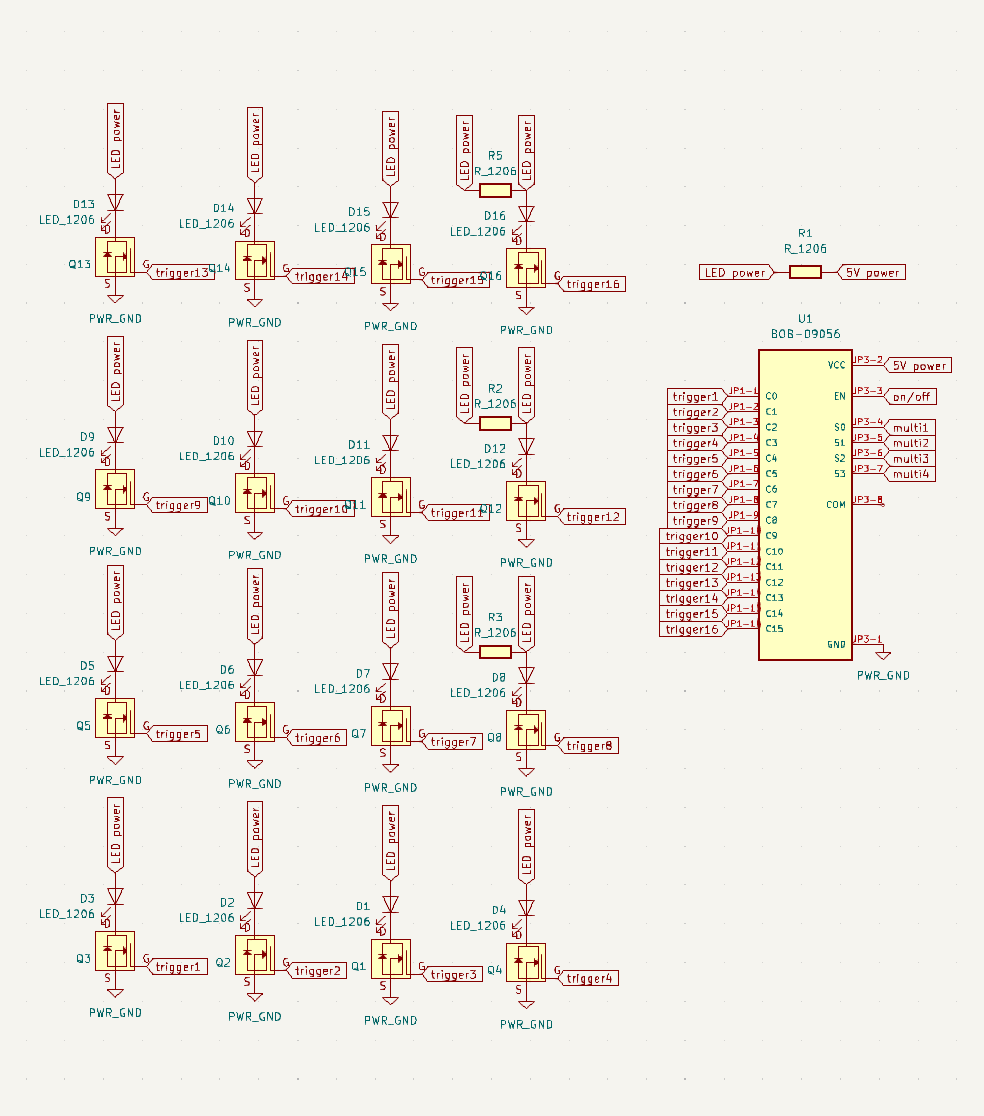
At first, this was what I was imagining as the scheme for my breakout board. I want a 4x4 array of transistors, each attached to an LED. I was thinking to just test this matrix with the basic surface mount LEDs that are available in the fab inventory, so that I can at the very least begin to program different pattern sequences through the multiplexer. This of course negates the need for the transistors, because the fab-supplied LEDs are rated for relatively low voltage / current, meaning that they can share a power supply with the multiplexer and the Xiao, and there is no need for a transistor gate to isolate the multiplexer/xiao power supply current from the LED power supply current. At any rate, I wanted to make progress toward my final, so decided to stick with the transistors and see how I could stuff a board with all of them there.
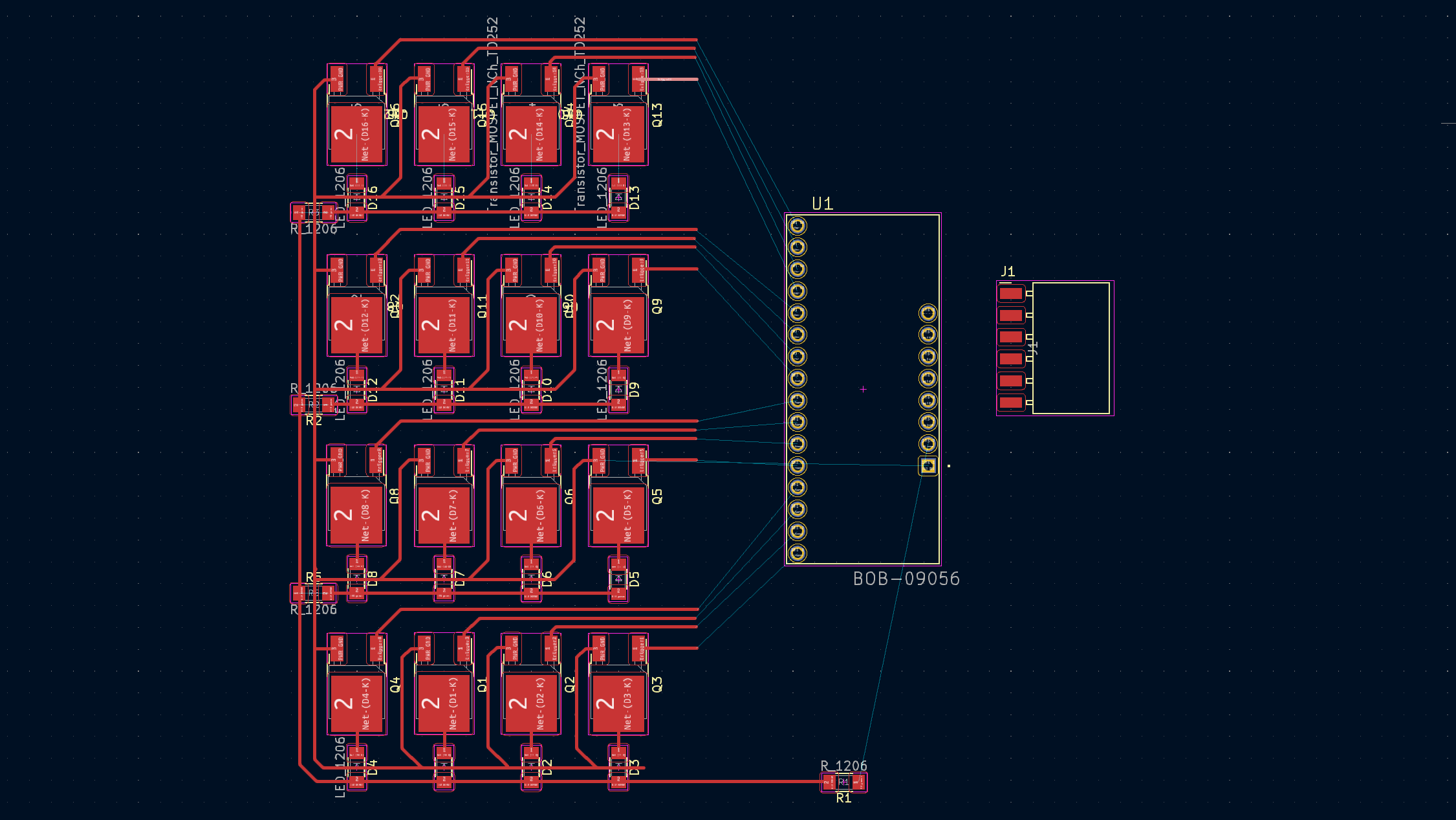
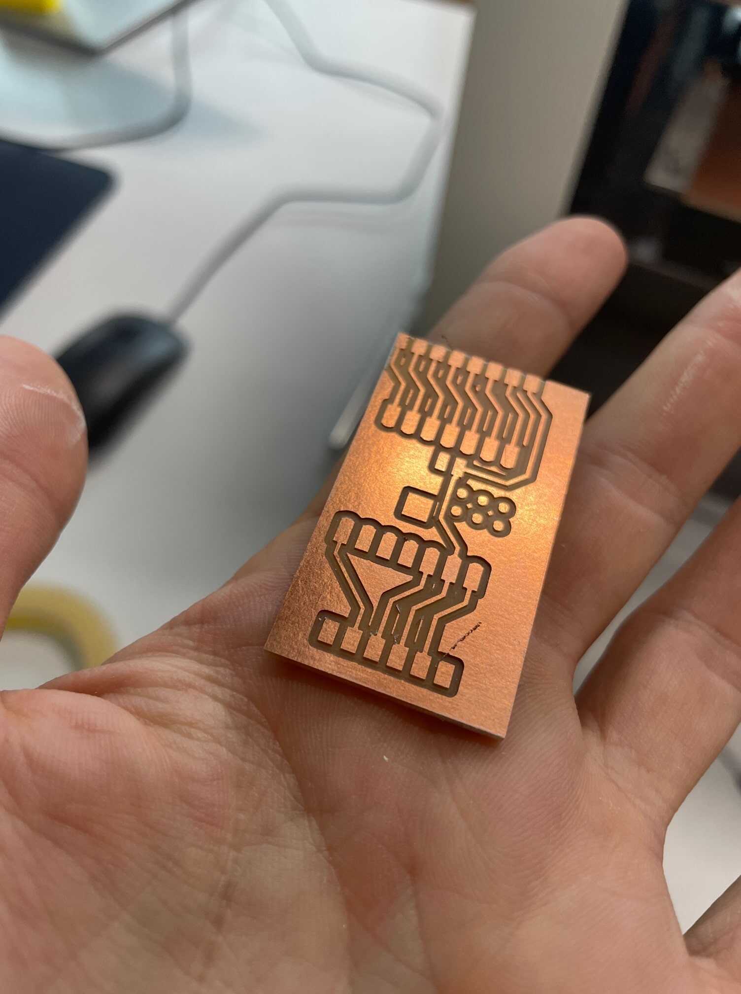
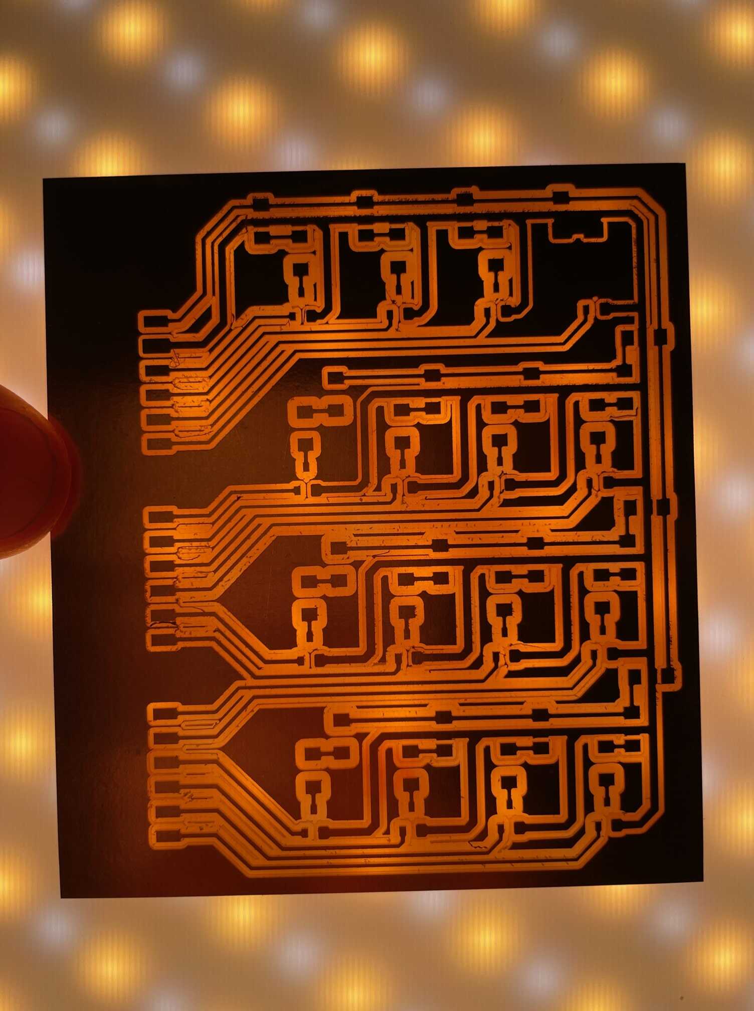
This is what the PCB design ended up looking like for this scheme. At first I was thinking that you had to attach a resistor to each LED, but then it occurred to me that since all the LEDs are connected to the same power supply, it would be redundant to use this many resistors and I would be better served by placing on further upstream that could service all the LEDs. Wrong! Doesn't work like that. Having one resistor upstream would have prevented me from being able to program each LED light individually, so this was going to have to change. I also didn't realize at first that the footprint I was using for the multiplexer was for this particular multiplexer's development board, not for the multiplexer itself. I thought that maybe this whole thing would need to sit atop the PCB, and be routed into place, but in actuality it can stand as an independent unit and be linked into this circuit through connectors. I ALSO found out that the transistor footprint I was using was unnecessarily large and that we have transistors that would be rated for more than enough of what I would need for this use-case that are much smaller / probably less expensive. Revise, Revise, Revise.
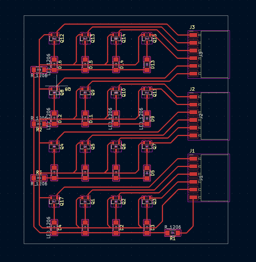
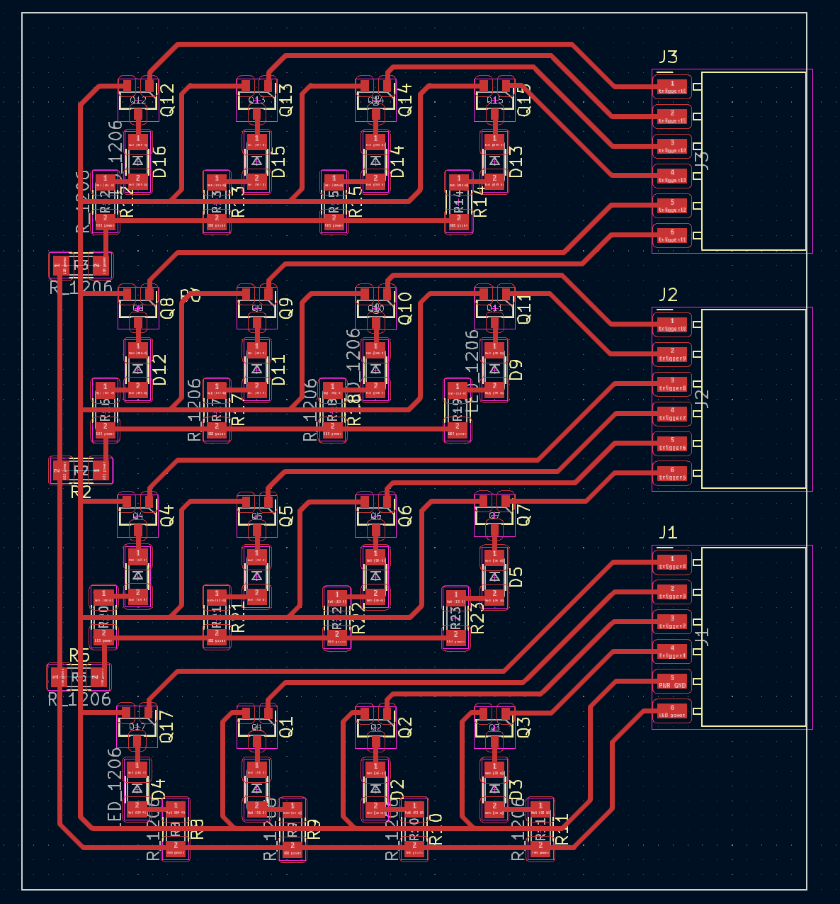
This is where I finally landed for my breakout board. It took a lot of back and forth, but I'm thinking it should do what I want it to do now. I think the struggle helped me wrap my head around the EDA software more and get a better sense of how to jump between a physical component stock and the digital design and figure out how to make each complementary with one another.
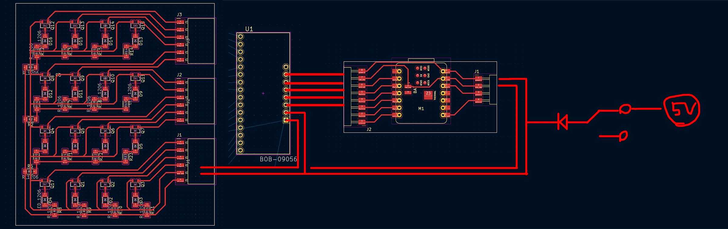
Okay, so this is the complete design: the development board, its dedicated power supply of 5V, its multiplexer and the multiplexer's breakout of 16 transistors/LEDs. When I eventually step this up to be 16 spotlights, I will need to included a voltage regulator between the power supply and the Xiao ESP32c3 to drop it down to a safe 5V. Time to start fabricating this!
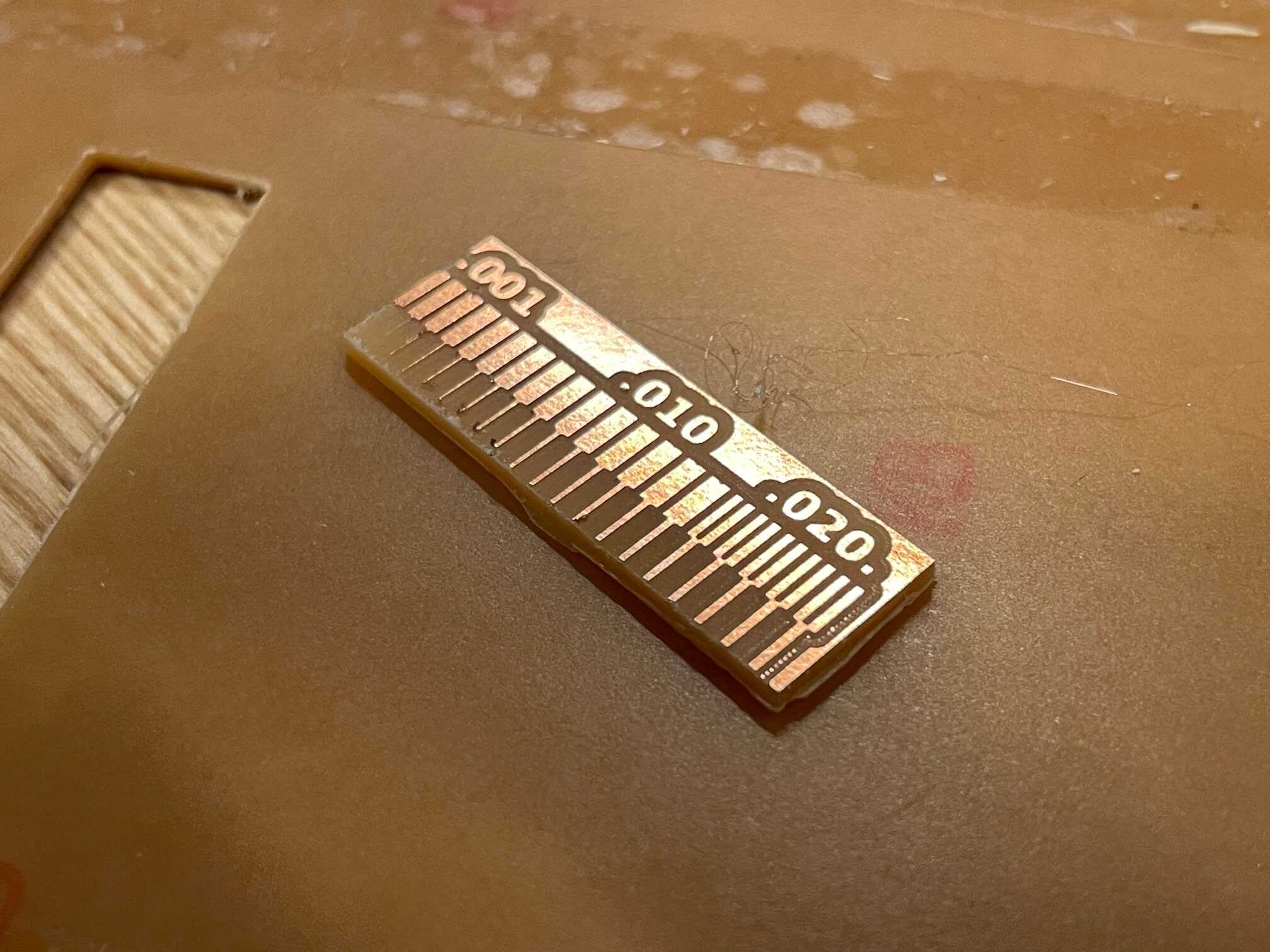
First step was, with the group, to mill a test print to get a sense of what detail the machine is capable of pulling off. We used our TA Leo's guide (https://github.com/leomcelroy/fab-notes/blob/main/MODS-SRM20.md) to figure out the user interface for the milling machine. These notes are great, expect for it didn't mention that you need to re-calculate the file after changing the home settings, so make sure to account for that. For internal widths it seemed like with a 1/64 endmill it wouldn't do anything less than .020. I went back to my schematic to double check that nothing is shy of this in my KiCad design rules, and moved forward.
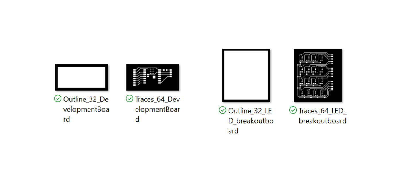
So first step is to get PNG files of THE SAME DIMENSION, out of KiCad. KiCad does not let you directly extract this file format. Instead, KiCad lets you extract a .gerber file, which you can then turn into a PNG using Quentin's super helpful website! (https://quentinbolsee.pages.cba.mit.edu/gerber2img/)
When you export your gerber files they will all land wherever you have your KiCad file stored, and you can place whichever files you have directly into the web browser one at a time. It's important to start with your outline file, which you use to lock the dimensions and aspect ratio before dropping other files into the browser. This way, all of your pngs for that particular PCB will line up on top of eachother when you are cutting them on the mill.
This is something I DIDN'T do the first time I used the software, which cause the cutout to slightly wander, cropping my 8 pin connector pads and making the board so that my microcontroller would not be able to accept a USB-C (Too much overhang).
After getting the PNG calibrated to the same dimensions (and my ever-changing design), I milled again. I ran into one more issues which I forgot to take a photo of but will include it here for the record, for some reason when I went to mill this board only half of the board was milling properly and the other half wasn't getting touched. It appeared that the plate was uneven, even though I had been very deliberate about making sure the double-sided tape backing was tightly pressed and cleanly done. I was able to fix this by playing around with the depth-cut parameters in MODS. This is directly under where you hit the diameter of the bit you are using. Normally these are presets, but you can adjust them to have bits cut more or less deep. I changed the 1/64 endmill from having a depth cut of .004 and max cut depth of .004 to having depth cut .006 and max cut .012. This was all it took to get a slightly deeper cut, and complete the board.
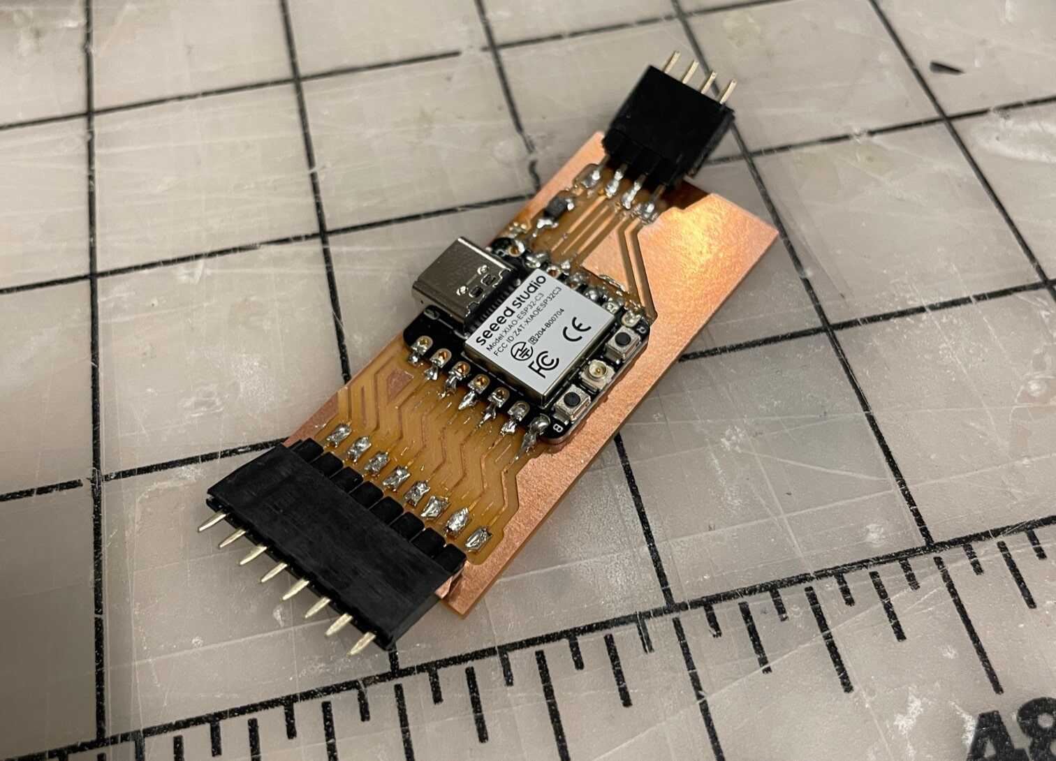
I headed over to the solder station and was confronted with another thing that I have never done before. It ended up being pretty fun, and ended up picking up a few techniques by the end of this small development board. One thing I caught myself doing at the beginning which was causing some coldish looking joints was after heating the pad and pin of the Xiao for 15 seconds, I was place to solder and it would melt, but then I would very quickly remove the soldering iron. This I found was not in my best interest. In future joints when I had left the iron there after melting for a second or two longer, the solder simply flowed across the joint, and I could quickly remove the iron leaving a shiny joint.
I found that while I designed the development board for horizontal pins, these pins are centrally localed within the connector casing and don't come down to meet the pad. This is an issue because it was seemingly too large a gap to bridge with solder. I decided to try to attach them at an angle, which worked suprisingly well? The solder is quite strong once it cools.
I was able to (almost) mill my development board in addition to this, but for whatever reason it failed to commit the last pass on the last module. I didn't notice this until I had come to solder it, not sure why it happened. Perhaps it's possible that a bit broke right at the end and I didn't notice since it was almost there.
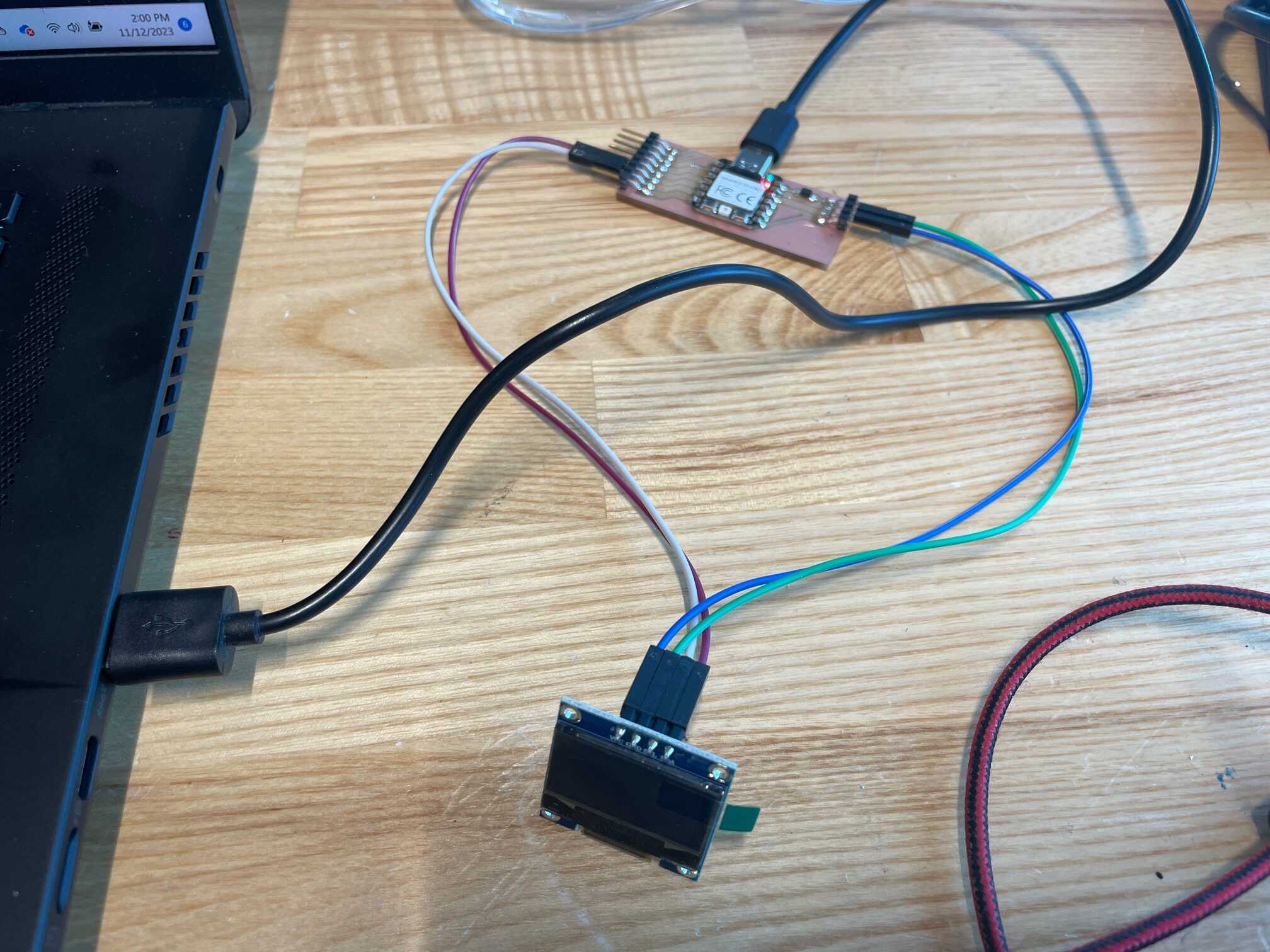
But at the very least I have this little development board complete, so I figured to satisfy the assignment I could just go ahead and test it with an OLED. The OLED just needs an SDA and an SCL, which if you look back at the pin breakout I have these pins broken out, as well as a 3.3-5V power source, and a ground. Should be good to go.