Moritz Kassner
Advanced PCB fabrication using the fab workflow
How to make a cuircuit board for almost any component. This tutorial is aimed at giving tips for advanced usage and shows how far one can push the fab pcb fabrication proess using the modella or any other pcb mill with comparable resolution.
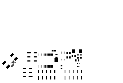
Making traces small - pushing the limits of resolution
Being able to create boards with sub small pitch is highly desireable for two reasons:
- access to smaller components and componets with very fine pitch
- more space for layout
Many bigger componets are only available in packages that require fine pitch routing, like the lvds deserializer in the larger package. Other comonets like the unbuffered inverter on the left, could be usefull because real-estate on a small board may be rare. Both pacakges have similar pitch and can be used with fabbed pcbs.
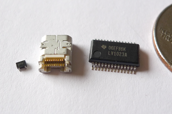
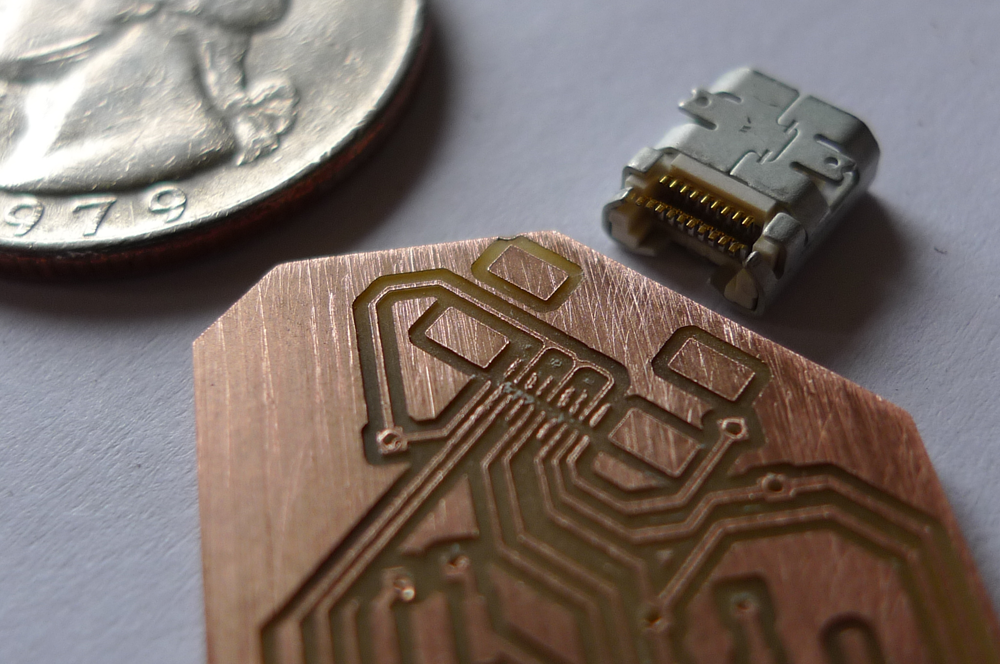
The mirco-dhmi connector in the middle has a 0.4mm (16mil) pitch. This is almost to small. the traces leading to this connector have to be thinner that the connectors legs, for the 10mil endmill to seperate them (pitch =0.5*max tracewidth + endmill diameter + 0.5*max tracewidth).
At 0.15mm tracewitdth the traces become extremly delicate, just the heatshock from soldering can delaminate the ends.
Reference Bed for easy double sided pcb fabrication
While single sided PCBs are easy to make, they quiqly reach their limites due to the fact the crossing are not allowed. One way is (exessive) use of 0 ohm resistors. Simplyfying the double sided production allows for more flexiblity in layour and routing
The bed is made by fusing two large stock pieces on the faces close to the edge. It is then fixated on the bed and stays their for its use life. Using this png a pocket is created by seperating the inside part and tacking it out.
This created a perfecly refereced bed that has no bias like a simple referece edge. Using this pcbs can be fabbed with hole misalignment smaller 0.1mm! The holes have be drilled from the back side.
The origin for board fabrication needs to be set to x = y = 12.7mm when using the referece bed supplied in this tutorial.
Fix fixation of the boards I prefer the transfer film that is stocked with the vinyl cutter, it has much better handling and reduces fab inventory diversity.
Adding Vias
With double sided layout comes the necessity for vias. The best way I found to connect a via is using the fab inventory wire. After twisting a piece is inserted through the bottom, soldered on top side, cut and soldered on the bottom side. This makes reliable vias, unlike throuhole resitor pins or solder wig.
Exposed pad qfn package soldering
This very common package usually has a pitch of 0.5mm. Using the above recommendations boards for this component can be fabricated reliably.
Soldering is possbile well:
- use flux (remember to clean your boards if you use water-soluble flux)
- alignment is crucial
- just tin the iron tip and swipe alongside the package edge, connecting each pad with its trace.
- if you have an "exposed pad" package (many are), the pad is extende up a bit and you can check connectivity, by touching the trace and the pad extension on the upper edge of the package with your multimeter leads.
- tip: 45degree alingment of the package may help for excape routing.
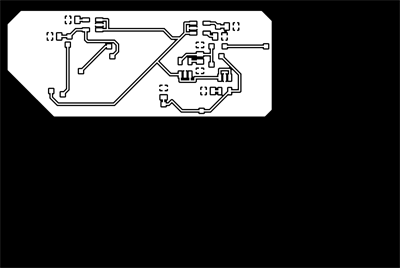
Automated Eagle to FAB-module png export
This is a refined version of Andy Burgandis eagle makefile:
Has to be located in Eagle project folder. It automaticly creates pngs of top,bottom,drills and board outline. The bottom layer is flipped and assumes that the user flips the board around the horizontal axis.

Outline

Drillholes
Top Copper
Soldermask
Bottom Copper
This script assumes that a new layer called "RefereceFrame" contains a recangle with the exacat dimentions of the stock. This is crucial for proper flipping when making double sided boards. The makefile can be found here