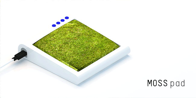
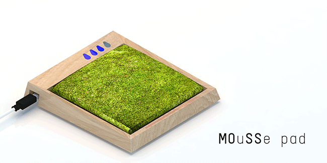
MOSS PAD
Final Project
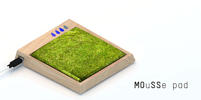
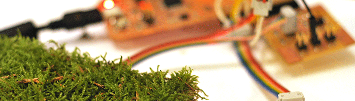
MOSS pad is a bio-based interface that replaces the cold, mundane track pad with an inviting, sensual plant interface. Through capacitive sensing user’s gesturers are translated to X,Y coordinates, and left and right clicking.

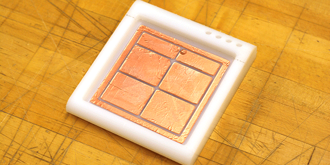
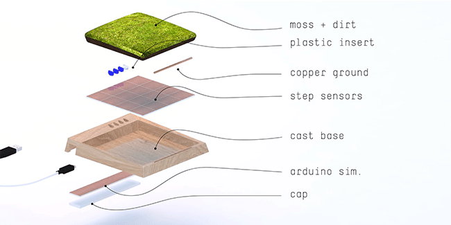
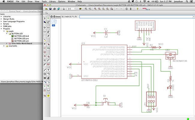
The system is composed of the components in the assembly diagram above. Key to the MOSS pad’s production is the use of the ATmega32u4 with built-in USB communication, which, when combined with the Arduino keyboard and mouse emulator library, allows the circuit to be recognized as a mouse input.
See Fableo below.
Data Sheet
Another fun feature is the ‘water me’ feedback. By calculating the average capacitance relative to the maximum measurement (saved to eprom) the top right LED array can warn the user when the moss needs watering.
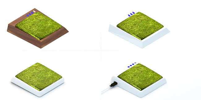
Multiple designs were developed. Ultimately, I decided on a technology-meets-moss scenario, something akin to Eva of Wall-E.
Rendering of final design.
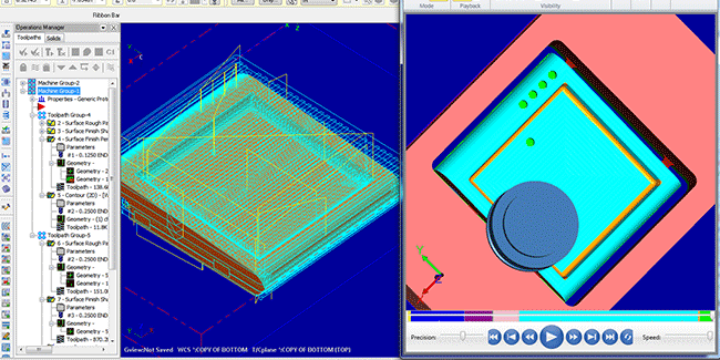
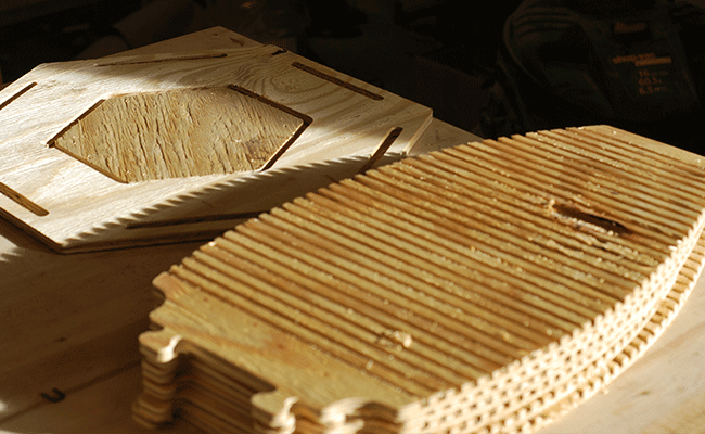
After much debate, abandonment, and doubt I decided to flip mill the base out of 1.5” HDPE on the GSD’s Track Mill, which has been NC retrofitted. The Track Mill was chosen because high level indexing, which allows for high precision milling and rigging.
Image above shows path planning in Mastercam using flipped work object planes - thanks Rachel Vroman?
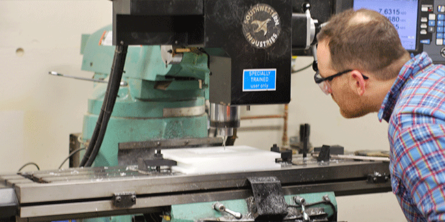
Milling, one major perk of the Track Mill is the capacity to drive the machine at any point. Here, Burton LeGeyt is cleaning up area’s the path planning missed. (This also saved me from a major flipping disaster).
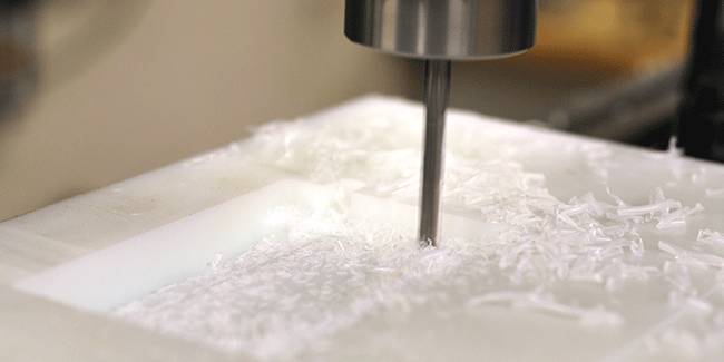
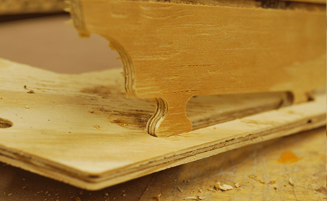
Detail image
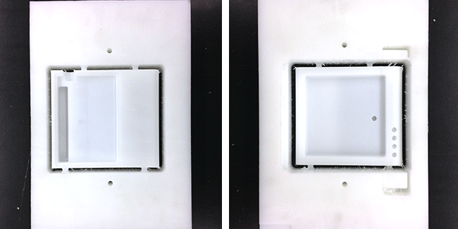
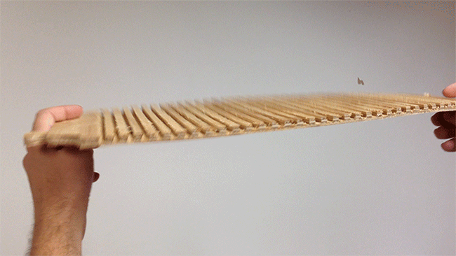
Finished piece, top and bottom with tabs.
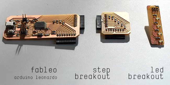
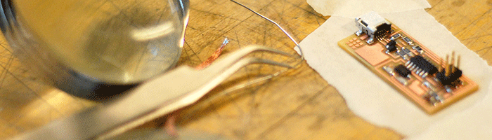
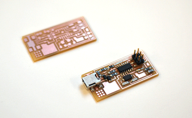
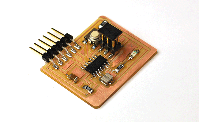
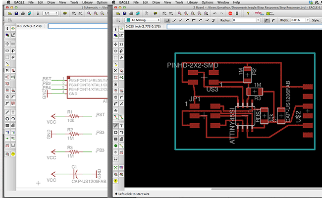
As mentioned, key to the project is the production of a Fab-Arduino Leonardo with an ATmega32u4. With some serious help from Matt Carney I was able to produce a working FabLeo. Eagle files, traces, holes and interior images can be found below.
FAbLeo
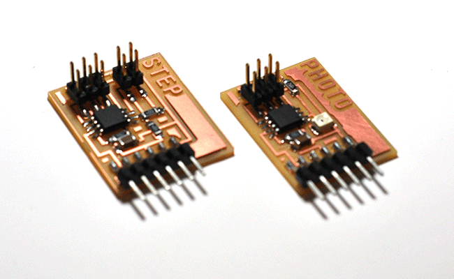
In Addtion to the FabLeo separate breakout boards were produced for the capacitance sensors and led array. In the case of the capacitance sensor a high signal is sent out across each pad (described below) then after a described delay the pad is tested through analog read to see how high the signal is or how much capacitance was in the pad, i.e. was it touched. Again, files found below.
Step Breakout
LED Breakout
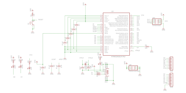
FabLeo schematic.
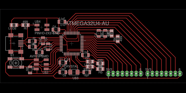
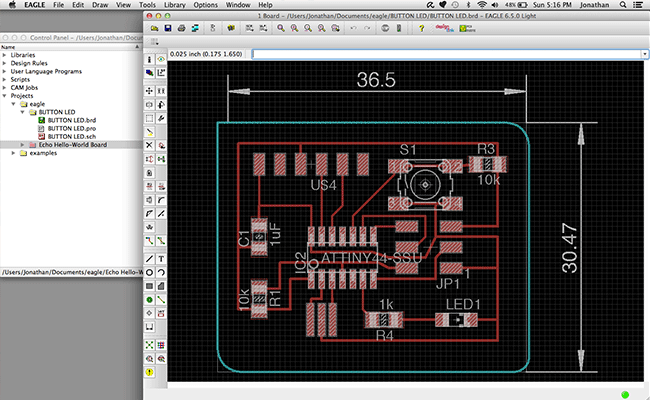
FabLeo board.
Vinyl cut copper pads. Interior transmit pads with a bounding ground pad.

Coding of track pad movement turned out to be relatively straight forward, each pad’s normative capacitance is tested at start up, from there increased capacitance can be measured and calculated against a threshold. The top two pads were coded as left and right click buttons. X,Y movement was calculated very simply by adding the pads X,Y value based on a standard quad system. For example if the top pad has high capacitance +X and +Y were added to the total X,Y movement (which is zeroed each loop). Therefore, if one is to touch both the first and second quad +X and +Y would be added to +X and –Y resulting in a +1,0 movement.
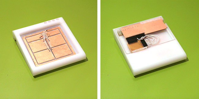
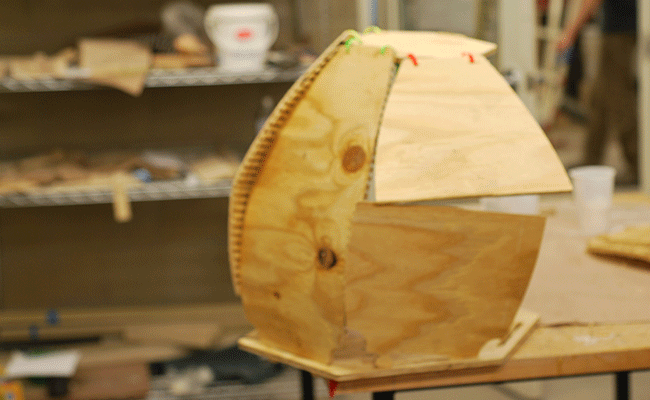
Final assembly, with via between copper pads and integrated circuits at the base.
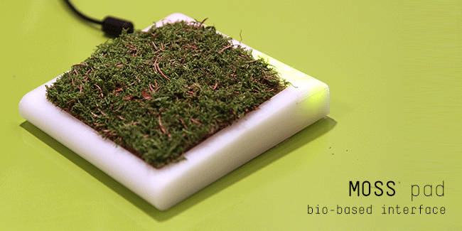
MOSS pad.
Early Tests.
Video of MOSS pad in action...more to come...hopefully
Parts list.
BACK TO THE TOP
Future Final+
Assignment One
This is an exploration into physical pixels applied to a double walled building envelope....
Idea Two...Testing of borosilicate glass, which is characterized by low coefficients of thermal expansionlow and softerning point. The idea being the potential to print glass forms.
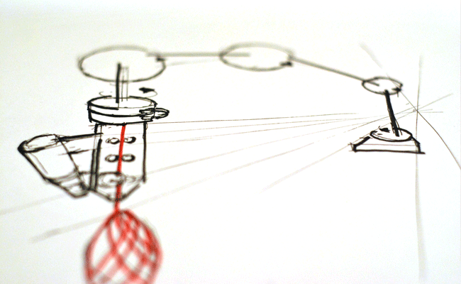
'Printing' or pulling of glass forms using six-axis ABB robot. This scope of the project would include making of tool head and potentially programming Rapid code through novel GUI. Tool fabrication would include, feed mechanism with stepper motor, contact or pressure sensor to detect rod termination or breakage, and resistance enduced heating element
Idea Three...Here is schematic for the now abandoned smart film project. The idea of this project was to cast a thin film with embedded solar cell, processor, supper caps, nitinol and FET based accuator system, IR networking, and push botton programming. These components would allow the films to respond to light levels and user override by folding open and close. The project was based on a robust research project into thermally actuated Flexinol shade screens, seen in the video below
Harvest Shade screen for Team Capital DC's solar home.
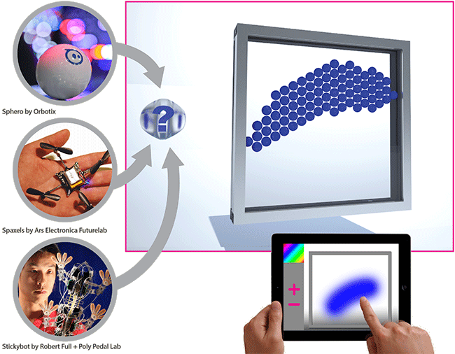
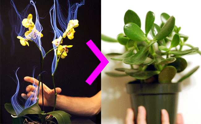
Idea Final...Given the fun I had with week 10's project, IMA Plant, I thought it would be good to shift my final project to a plant based track pad. I surveyed friends online this afternoon and all agreed, having a piece of moss, or any other plant, instead of a mouse would be a nice experience.
The idea is to use stepp response to measure capacitance across an array of sensors and track movement. Given that the arduino leanardo can be used as a mouse or keyboard through embedded libraries translating movement and clicks should be 'relatively' straight forward. Another feature will be a 'water me' sensor and led display. Since the capacitance is inherently testing the conductivity or wetness of the soil, adding additional code that establishes a wet and dry feedback should be 'relatively' straight forward. Fabrication will require the items called out in the images above....
BACK TO THE TOP
Press Fit
Assignment Two
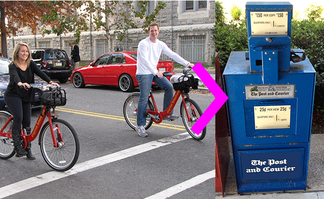
The press-fit concept is derived from an observed need for low cost single to multiple use bicycle helmets for City Share, Hubway, Citi Bike etc. The basic concept is that helmets could be provided as a kit of parts that users self-assemble.
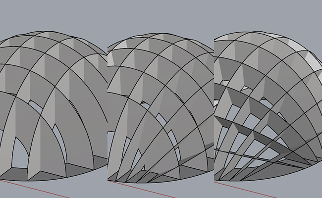
Multiple design strategies were developed based on a lattice structure. Though the optimal arrangement would be an orthogonal grid, a bi-radial array was chosen to reduce clash points. This choice will also result in complications during assembly …
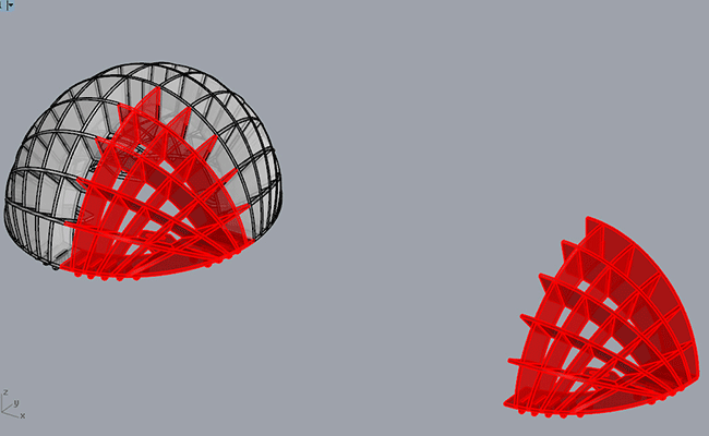
Given that the form of the helmet is an ellipsoid with bi-axial symmetry, a ‘block’ design approach was adopted. Each block (red) was designed then copied and mirrored into the other three quadrants allowing the block definition to be updated and populated.
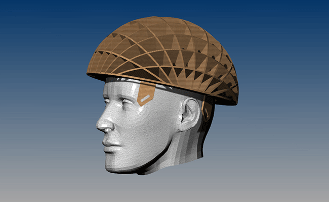
Rendered screen capture of helmet design on manikin’s head. The manikin’s head was used for proper sizing (to my large head!).
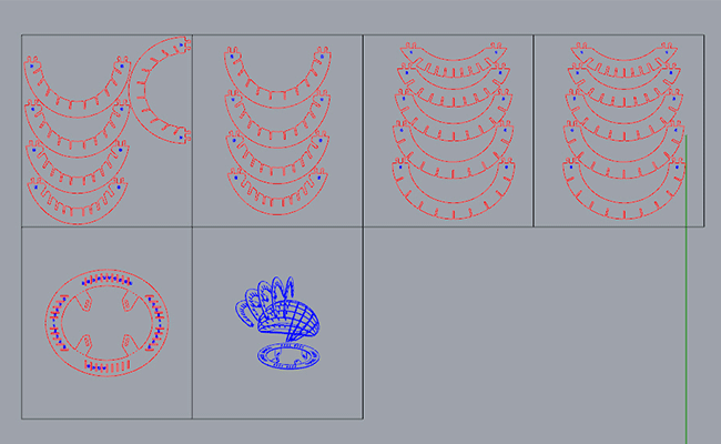
Laser cut file. Parts were assembled on sheets to allow each part to remain in the sheet via two small ‘tabs’. The idea being that each sheet could be stack, packaged and delivered.
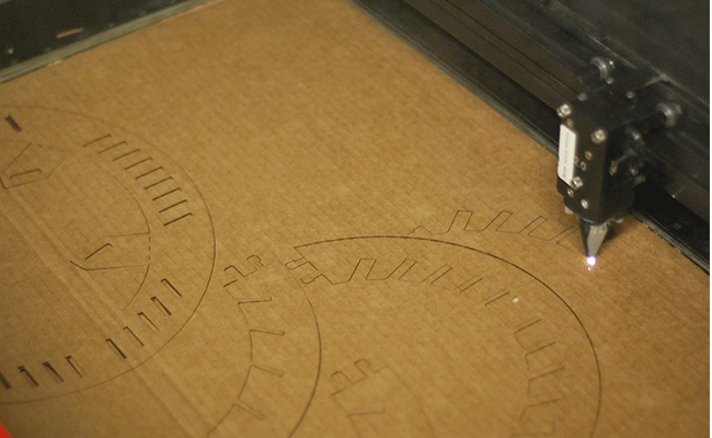
Parts being laser cut. I used the GSD’s 60 Watt Universal Laser Systems machine. Cut lines were set to 75 percent power, 30 percent speed, 500 ppi. Score lines were set to 10 percent power 50 percent speed, 250 ppi.

Detail image of tolerance needed for non-orthogonal lattice structure.
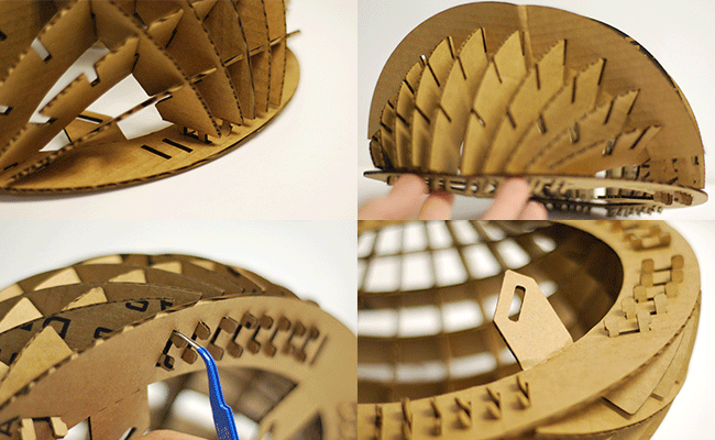
Images of issues encountered. Top left, press-fit tabs required small, nimble fingers making final ‘snap’ very difficult. Top right, as mentioned the bi-radial array meant that each parts alignment was off resulting in a bending of members when being assembled (FAIL!!). Bottom left, nimble fingers are replaced with tweezers, tabs also crush very easily. Bottom right, a chinstrap holder was folded out of the base ring along a dashed cut, which was not a clean fold.
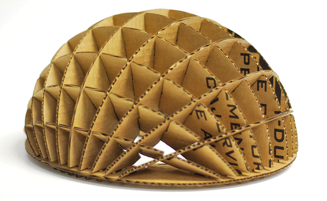
Final constructed helmet.
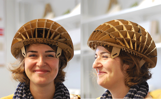
Though the project has many issues, it did provide a great opportunity to embarrass my new office mate!

Final reflection. Goal, technically effective helmet. Context, hipster sheek society. Reality, nobody picks Toad on Mario Kart!
BACK TO THE TOP
FabISP In-circuit Programmer
Assignment Three
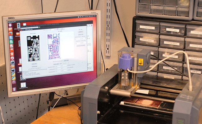
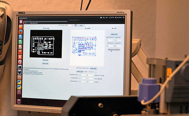
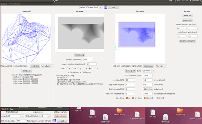
First step, machining the PCB using Roland Modella CNC machine and the associated Fab Module. Setting up the Roland Modella requires a series of 'rough,' hands-on steps:
1)Clean the waste board.
2)Adhere FR1 board with double stick tape (3)
3)Set specified end mill in chuck with setscrews (2)
4)Locate FR1 boards 'X,Y' '0,0'
5)With a tight grip, loosen chuck setscrews and lower end mill to Z axis '0' at the top of copper surface
6)Set end mill
7)Send RML file via Fab module:
Trace
Interior
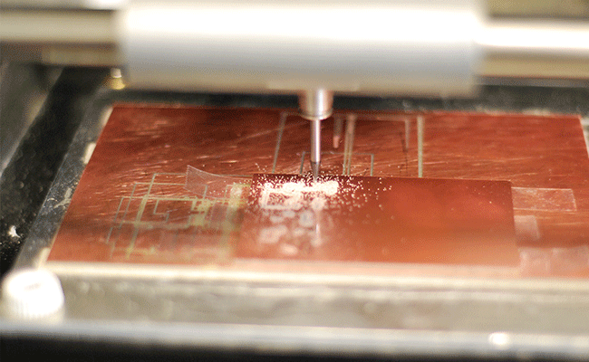
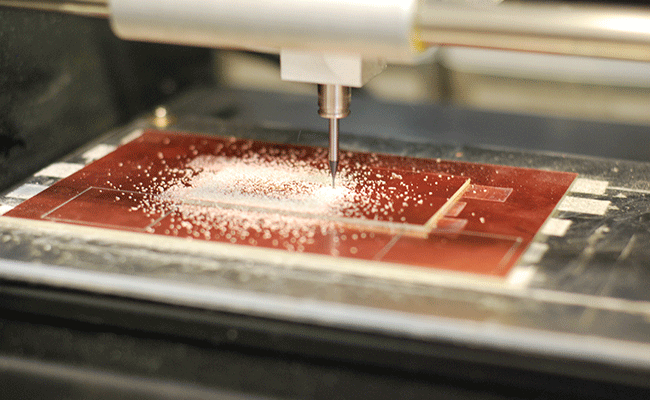
Roland Modella Machining trace path, note a 'pinkish' chip as a result of coper and white paper
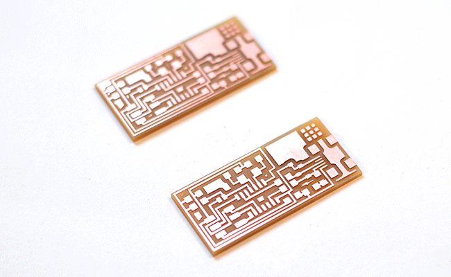
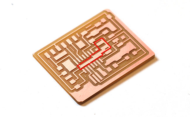
Finished ISP board. Washed with water and soap. I made two....to be safe.
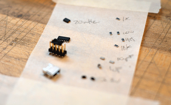
Stuffing the board. Great tip from the pros - before stuffing, layout and label all components on tape.
Board
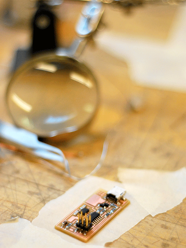
Finished ISP, just needs a bath to remove the flux
Finshed ISP
Programming the ISP using CrossPack for Mac OS and the Fab Firmware
Programming complete. Time to desolder and begin programming the next project.
BACK TO THE TOP
3D Scanning and Printing
Assignment Four
Given the more automated nature of assignment four, I choose to approach both scanning and modeling through web-based platforms.
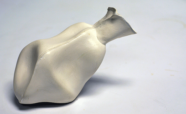
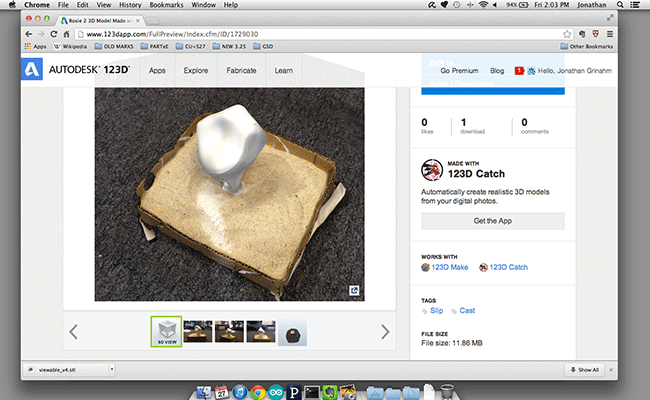
For the 3D scanning exercise I choose a ceramic slip piece designed by artist and friend, Rosie Midyette. I thought the complex surfaces of the three-part molded slip cast would prove to be an nice challenge for Autodesk's 123 Catch photomerge software...I was right http://www.123dapp.com/catch . Also note that the Iphone App would not download – possibly due to OS upgrade.
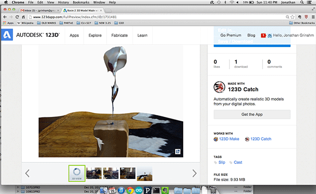
Screen capture of the Second attempt – first attempt failed. 3D scan was severely deformed on account of the multiple undercuts, assumed poor site of the piece, and homogenous surface texture – not to mention a 36+ hour turn around time.
Screen capture of the third attempt. Somewhat more effective, though bottom undercuts did not mesh/render.
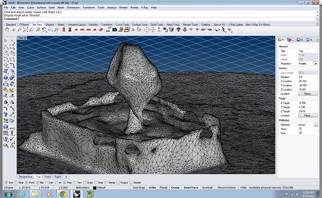
3D scanned mesh in Rhino modeling environment.
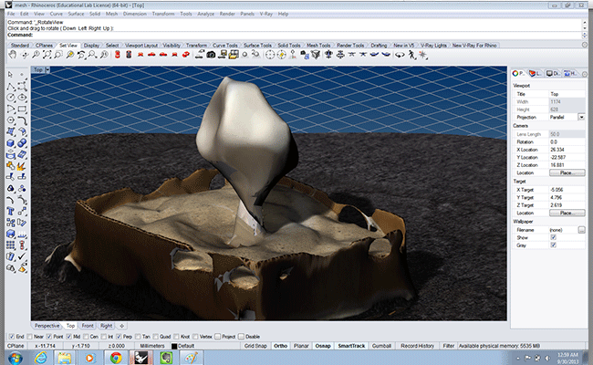
3D scanned mesh with texture mapping in Rhino modeling environment. Downloading files as ‘mesh package file’ provided seamless interoperability with Rhino via .obj format.
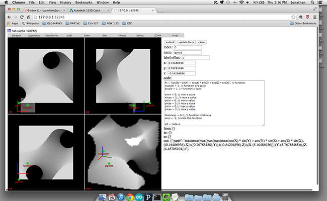
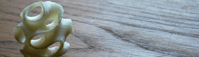
To produce a form that could not be fabricated by traditional means I choose to produce a gyroid, triple-periodic minimal surface (yes, I know it’s over used!).
Maintaining the web-based narritive I choose to model the surface using the Fabmodule Fabserver, and Frep modeling interface. A few key notes to installing and using the Fabserver module:
1)First download the modules and install the proper elements from the Fabmodule site, http://kokompe.cba.mit.edu/downloads.html
2)Once installed open the terminal and type : fabserver 12345
3)This should return the message : listening to port 12345
4)Then open Chrome and go the local server at URL: http//127.0.0.1:12345
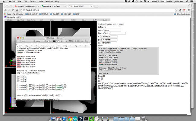
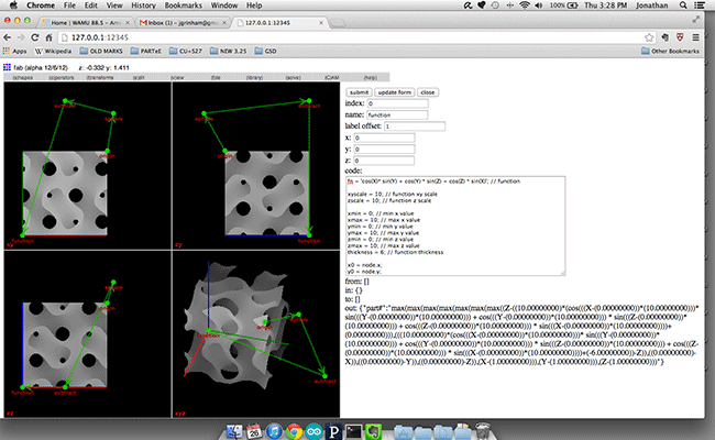
Producing functional nodes was quite intuitive and controlling parameters was simple. All and all it was a smooth process, however, since it is an alpha version and to my knowledge files cannot be saved, I recommend keeping a notepad open to copy functions incase of loose of connection or crash!
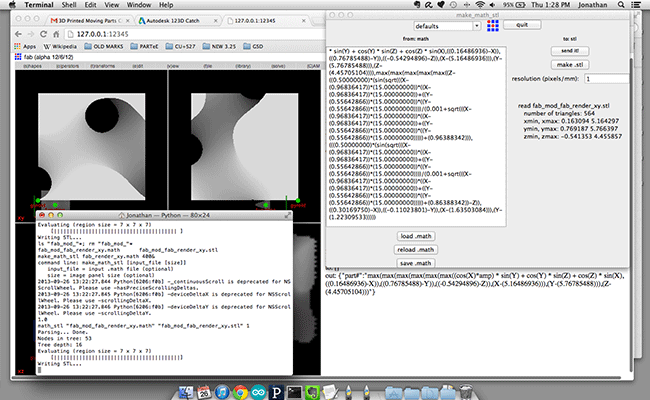
Exporting the geometry was an issue. I used the UI Cam>Fabricate to call the .math_stl module. The stl processed for hours, but did not return a file…
Last, I tried to explore a few Boolean operators, but had limited luck...
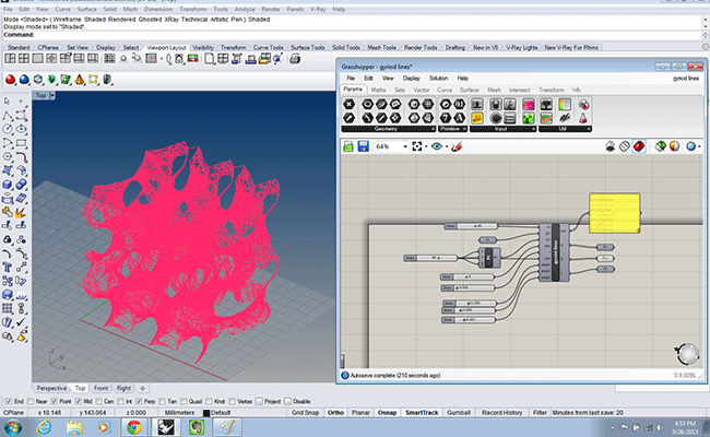
To produce a .stl file I resorted to Rhino/Grasshopper to translate the Frep Function into a Brep mesh – here is the initial meshing
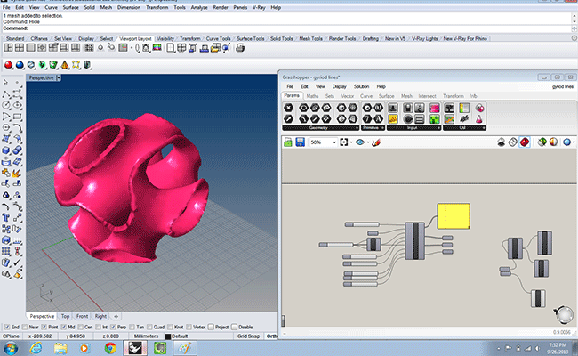
Final mesh with the help of Giulio Piacentino’s Weaverbird http://www.giuliopiacentino.com/weaverbird/
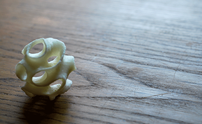
Final ABS print
BACK TO THE TOP
Computer-Controlled Machining
Assignment Five
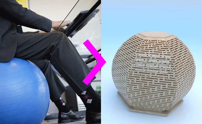
For this week's assignment I wanted to produce a non-standard readings of plywood - a volume and a spring. I also decided to tackle the ubiquitous gym-ball-office-baller.
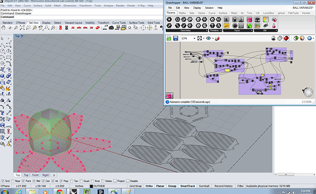
Geometry was parametrically modeled in Grasshopper for Rhino. The definition unrolled the spherical volume and allowed for versioning of tool paths, which were intended to produce flexure moments along the surfaces. For this prototype (and based on the plywood available) I decided to use a straight, continuous path, removing material at 1/4 inch offesets and leaving the bottom ply as a flexible surface.
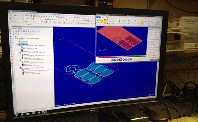
Tool paths and G code were generated and posted using MasterCam 7. Tools and rates included:
-1/8 inch dia. drill
-1/4 inch dia. Two flute flat end mill at 1600 rpm (reduced to 75percent)
-3/8 inch dia. 2 fluted compression flat end mill at 1800 rpm.
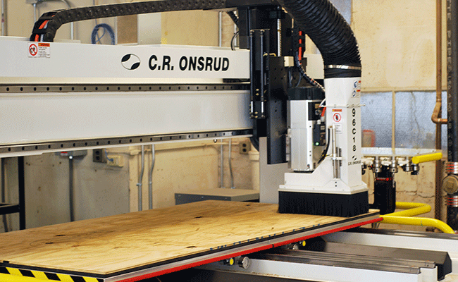
Onsrud 3 axis mill at work.
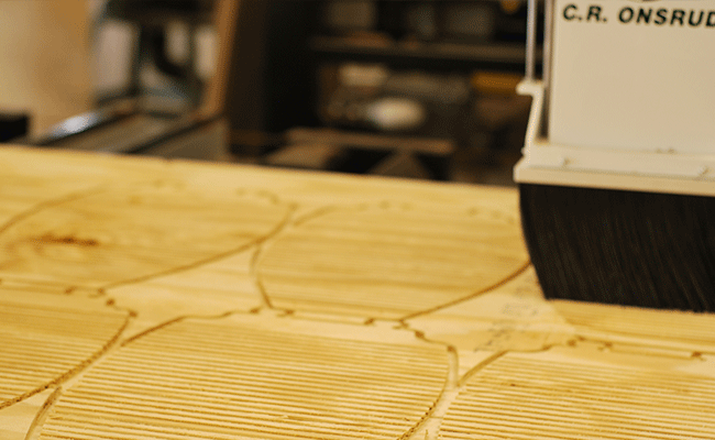
Cut path detail image
Final pieces. Left, base and top plate. Right, petals (6).
Demonstration of flexure.
Detail of snap fitting at base.
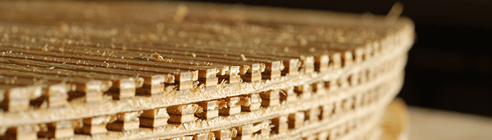
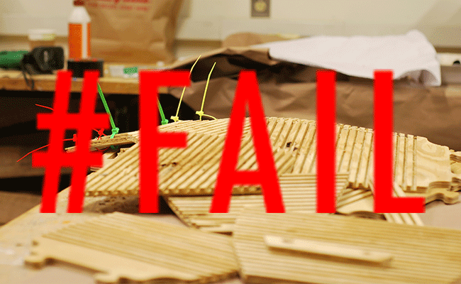
Failure. The final prototype failed as a result of multiple factors. The primary factor is assumed to be the quality of plywood. Multiple fractures and knots along the plys produced a non continuous surface on the exterior ply, which was intended to be the main structure. These defects, combined with the poor assumption to position the petals perpendicular to the ply’s grain, resulted in immediate failure of multiple pieces and final failure of all pieces during assembly.
Round two?
BACK TO THE TOP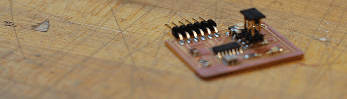
Electronics Design
Assignment Six
This week’s assignment provided a first time opportunity to use Eagles for circuit design and layout. Using Eagle was fairly intuitive, especially when using the fab parts library. After some experimenting, I found that named comports made the schematic design easier to manage.
Much like schematic design, board layout was fairly intuitive – though unused paths seemed redundant at times. I found it helpful to change the grid spacing in GUI setting to make object snapping more accurate.
Monochromatic PNG at 1600 dpi in the fab module.
Modela milling.
The initial design did not cut multiple paths that were too close for the 1/64 inch end mill, which required a quick redesign in the shop.
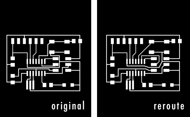
Updated interior traces.
Final stuffed board with button and led
BACK TO THE TOP
Molding and Casting
Assignment Seven
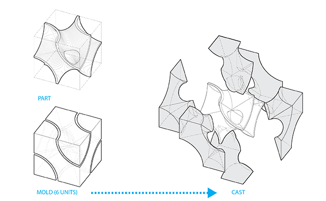
For this week's assignment I wanted to follow up on the 'complexity' question during week four's 3D printing assignment. During that week I produced a triple-period surface using the fab module's FRep solver. For this week I want to see if the same, or similiar surface could be produced via casting. *this assignment also rehashes a previous investigation.
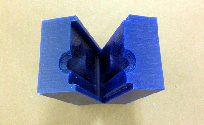
To produce the triple-periodic surface a six part mold will need to be produced.
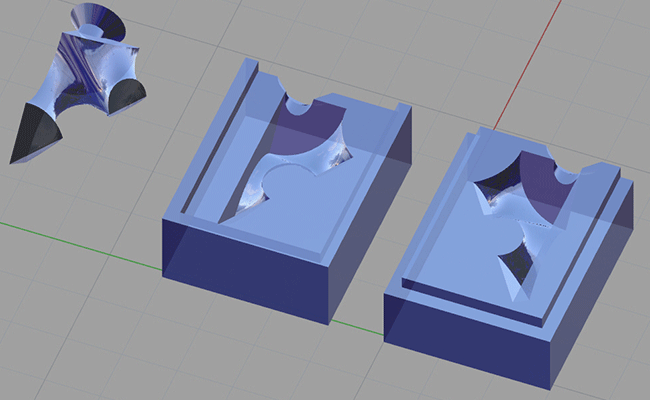
The two part mold of a singular element of the six-part mold was modeled in Rhino3D. Left, the intended final piece(s).
Mill of the two halves was done through the fab modules. The import .stl to .png solver work smoothly. Though, as we will see in the next image additional steps were taken to increase the surface resolution.
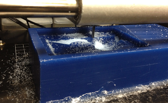
Milling on Modela
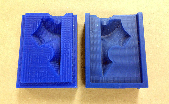
Final two-part mold. Left, with a default finish step over at 50 percent bit diameter. Right, with an increased step over at 80 percent bit diameter.
Nesting of molds.
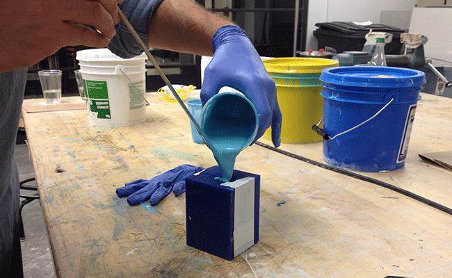
Pouring the mixed Oomoo 30 silicon rubber
MORE TO COME
BACK TO THE TOP
Embedded Programing
Assignment Eight
First, I attempted to make and program the ATtiny blink board following the tutorial instruction for the hello word program found HERE
Following the three steps below:
First, program the board
make -f hello.ftdi.44.echo.c.make
Next, load the code
make -f hello.ftdi.44.echo.c.make program-usbtiny
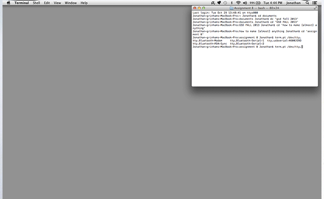
Finally, open the serial port connection window in python
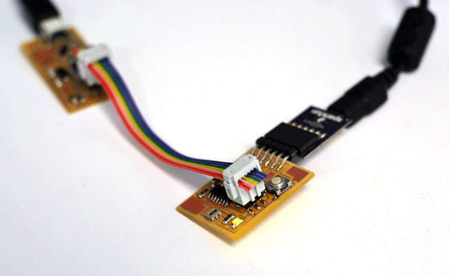
term.py
The programmer uploaded the C program file, however, when attempting to read the serial via the python monitor the board would show with out an attached baud rate and without opening the monitor.....after a few different downloads and attempted fixes I moved to arduino.
Programming using Arduino IDE
First, Download Arduino and install.
Next, Install FTDI libraries * in this case I used a FTDI breakout from sparkfun.
Next, Install the ATtiny board.txt library, found HERE
Create a ‘hardware’ file under in the arduino scretch directory (under documents>ardunio for mac users) and paste the ATiny Board.text within an ATtiny file.
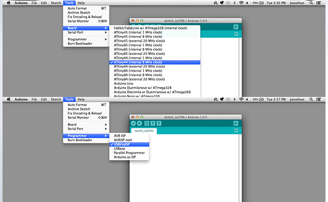
Next, select the board from the dropdown menu tools > board > ATtiny 44( internal 8 MHz Clock). (top image)
Next, select the ISP programmer from the dropdown menu tools > programmer> USBtinyisp. (bottom image)
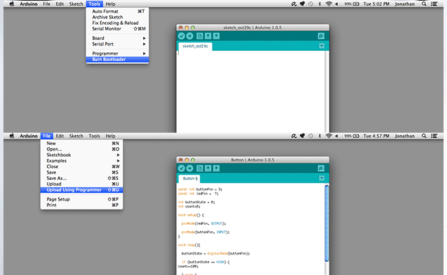
Next, burn the Bootloader from the dropdown menu tools > Burn Bootloader.
Finally, upload code either by using the upload button in the arduino environment, or the dropdown menu Filet > Upload Using Programer.
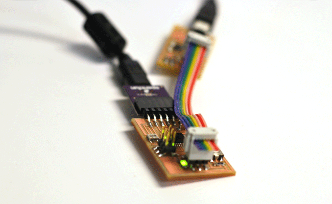
Play, but not too hard. Here I loaded a simple code that would increase the frequency of ‘ON’ signals to the LED the more I tapped the button, and then as the time between tapping decreased the LED would slow to ‘OFF’.....I got into it and broke the board.......on to the FABDUINO!
For the fabduino I wanted to start with the original board in expectation that this will not be the last one.
I used the board layout and traces and interior bitmaps from the class page HERE
Initial programming of the board through the Arduino bootlegger proved problematic. After many failed attempts, and a declared Fabduino time-of-death at 5:58PM. I forced my hand and loaded a new board.txt file to the arduino hardware directory established in the above description.
The original board.txt file found HERE
This file was first set up for the Atmega168 and need to be updated for the Atmega328P. Here is the final file with updates:
abduino2.name=Fabkit/Fabduino w/ ATmega328 (internal clock)
fabduino2.upload.protocol=stk500
fabduino2.upload.maximum_size=30720
fabduino2.upload.speed=57600
fabduino2.bootloader.low_fuses=0xe2
fabduino2.bootloader.high_fuses=0xdd
fabduino2.bootloader.extended_fuses=0x00
fabduino2.bootloader.path=arduino:atmega
fabduino2.bootloader.file=ATmegaBOOT_168_atmega328_pro_8MHz.hex
fabduino2.bootloader.unlock_bits=0x3F
fabduino2.bootloader.lock_bits=0x0F
fabduino2.build.mcu=atmega328p
fabduino2.build.f_cpu=8000000L
fabduino2.build.core=arduino:arduino
fabduino2.build.variant=arduino:standardv
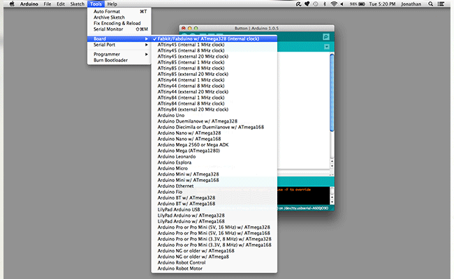
To burn the bootloader and programmer I then repeated the steps above selecting the Fabkit/Fabduino w/ ATmega328 (internal clock) board.
*note typically requires loading from programmer.
Time to program.... ATmega328P Data Sheet
.
BACK TO THE TOP
Composites
Assignment Nine
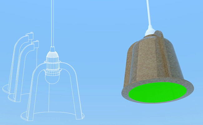
For composites week I decided to embrace both economy of the burlap fiber-base and a nearly inevitable return flange. This particular design is based on a stacking lampshade for a standard IKEA Hemma pendant.
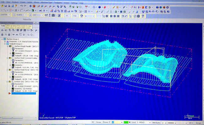
G-code for the two-piece mold was first programmed for the Onsrud router using Mastercam.
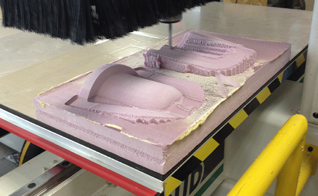
Routing of pink foam.
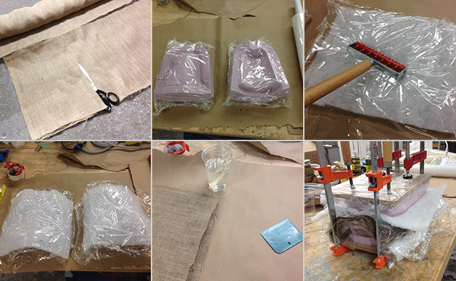
Casting composites requires multiple steps, read from top left to bottom right:
First, cut burlap to molds bounding area.
Next, insulate pink foam from epoxy using cling-wrap and spray release.
Next, cut burlap to mold’s bounding area (4).
Next, cut bleed (2) to bounding area a perforate cling-wrap cover.
Next, apply bleed and cling-wrap.
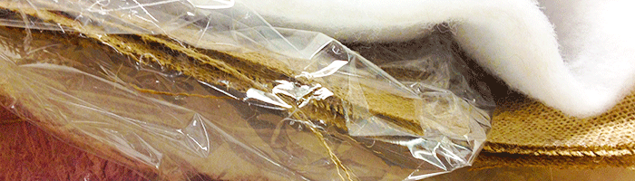
Next, mix epoxy matrix based on instruction, in this case 2-1, and apply to each layer of burlap with squeegee (4).
Last, lamp male and female mold with top and bottom bleeds.
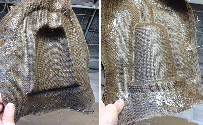
Final, untrimmed form ( one of three).
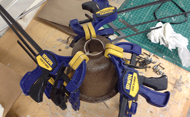
Bonding.
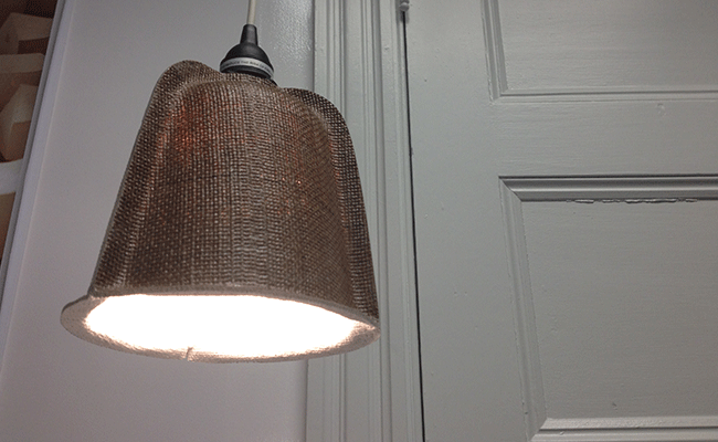
Final.
BACK TO THE TOP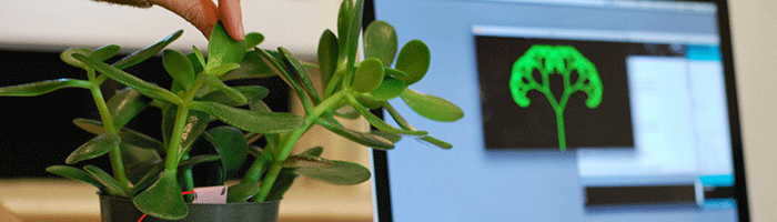
Input Devices
Assignment Ten
This week's assignment, input devices, provided the opportunity recreate Disney Research’s Botanicus Interacticus, interactive plant project.
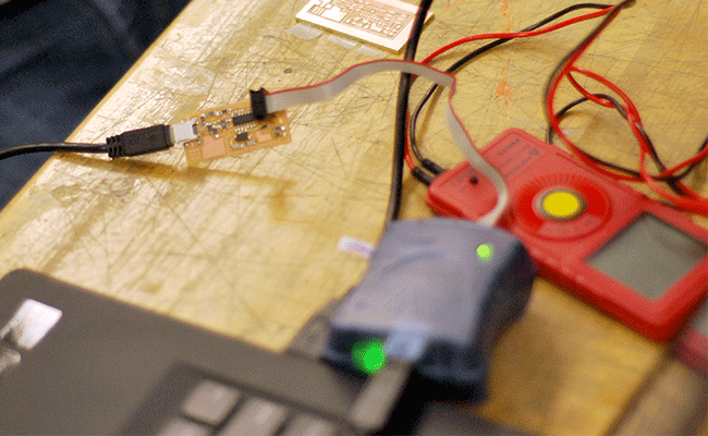
To begin, I ‘redesigned’ Neil’s step response board in eagle – though I ended up milling his original board to provide a control when testing the system. This was more of refresher, skill builder.
Final board(s). I milled and stuffed a Phototransistor circuit as well, it works great, but didn’t excite me the way a plant and some copper plates could.
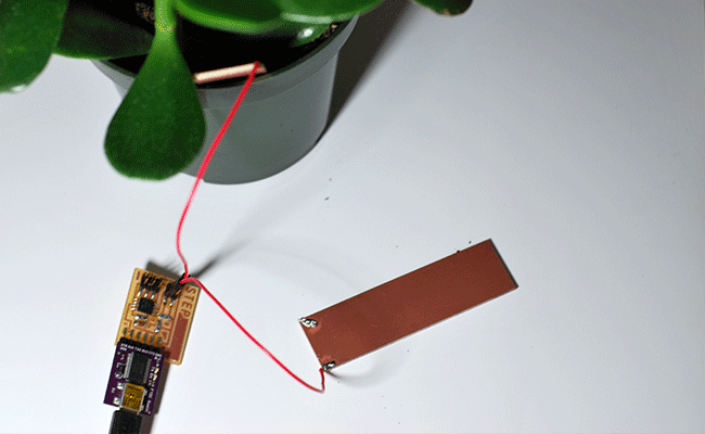
To produce a response via interfacing with the plant a copper plate is placed in the soil and second plate is exposed to produce the ground or signal input. By ‘stepping’ the output signal through the soil plate and reading the ground plate the systems capacitance can be read. In this case the plant, plates, and user produce a loop, as the user touches the plant the loop is closed, and based on the force and location of touching along the plant the capacitance changes. In this case, even a hovering hand will produce a reading.
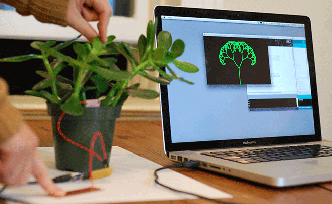
Programming the board began by making the Hello.txrx.make file and uploaded Neil’s original Hello.txrx.c code using the Arduino IDE. With a few tweaks to the original code could be read in Processing. Using this data, I then applied capacitance value to an angle calculation within a simple L-system tree sim.
Video of processing interfaces
BACK TO THE TOP
Output Devices
Assignment Eleven

This week's assignment, output devices, provided the opportunity to bang my head against the wall and waste away many hours because of one small missed fact...ISPs do not supply power...
Lesson learned, solution provided. I added a toggle switch to my ISP board that allows power to be supplied to the board being programmed, or turned off when power is supplied via another source.
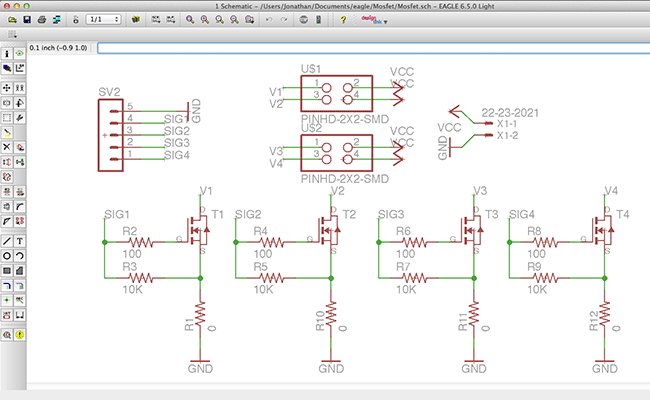
The intention of my time was to develop a few hello world test boards, then design a stand alone, MOSFET break out that could be used for Nitinol wire and a Fabduino (above).
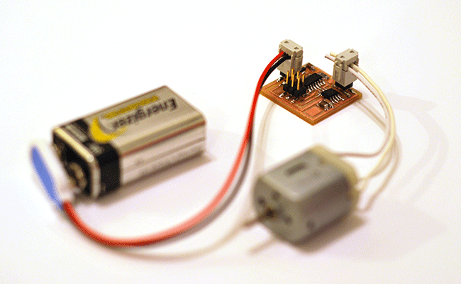
Since countless hours were lost trouble shooting a non-existant problem on each of my boards, I wrapped up this weeks assignemnt by testing codes for a DC, Stepper, and Servomotor.
Above, a DC motor programmed through Arduino IDE
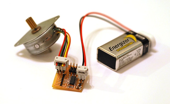
Stepper motor programmed through Arduino IDE
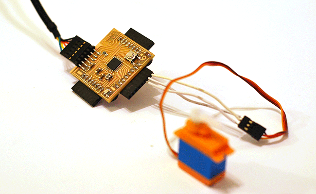
Servo motor driven by Fabduino, programmed through Ardhino IDE
Nitinol wire being actuated using MOSFET control via stepper board.
Video of devices
BACK TO THE TOP
Networking and Communication
Assignment Twelve
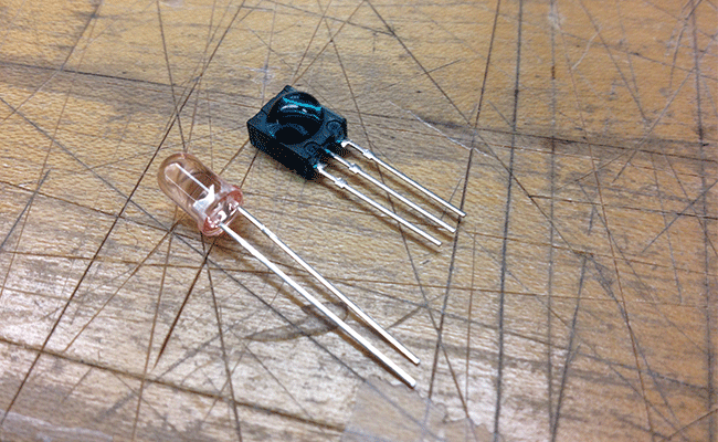
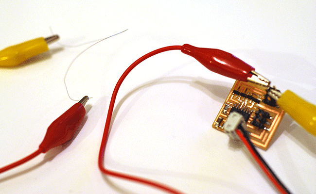
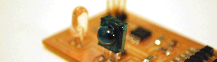
This week's assignment, output devices, I attempted to produce an infrared network communication using a standard IR LED and an IR sensor provided by Jeff, found HERE
My assumption was that this would be a simple swap for the physical BUS connection in the HEllo.Bus.45 example. And that the code could be used with some tweaks, including pulse modulation at 38khz...needless to say, it is still a work in progress.
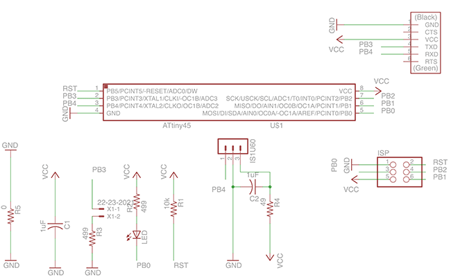
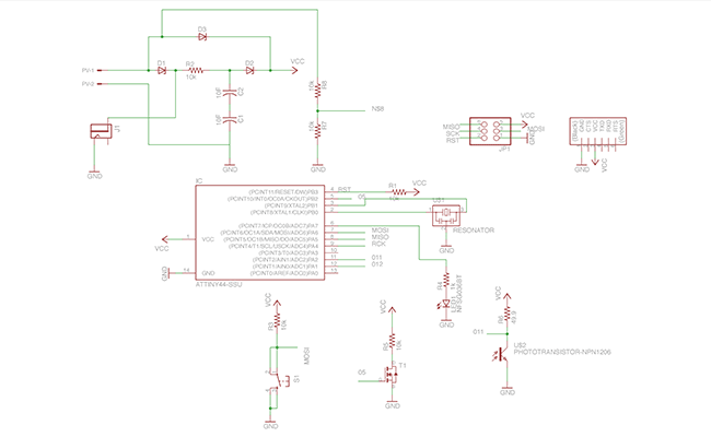
Schematic design of master controler with IR sensor and IR LED connected to the RX and TX ports and an FTDI header for serial communication.
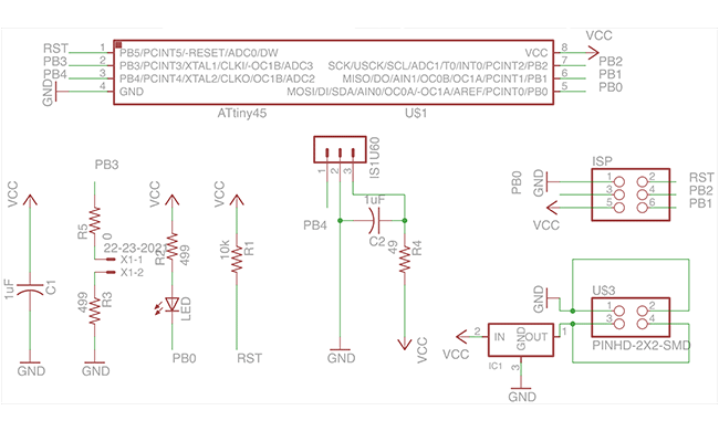
Schematic design of a node unit with IR sensor and IR LED connected to the RX and TX ports and a header with voltage regulator for external power.
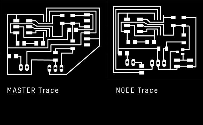
Traces of master and node.
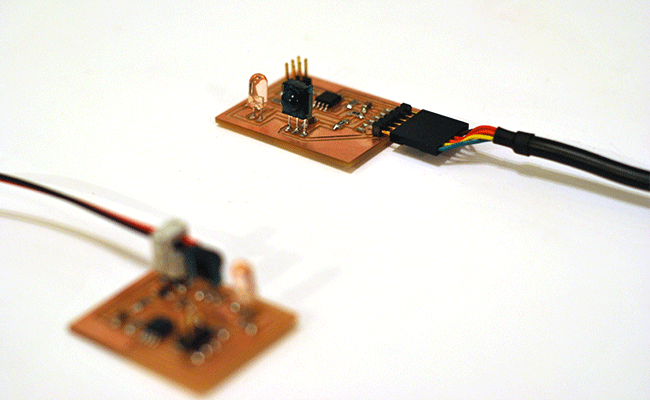
Master and node boards. Both boards will not program, I assume, since the node is a design version of the master, that there is short in the shematic layout of both boards...time to debug.
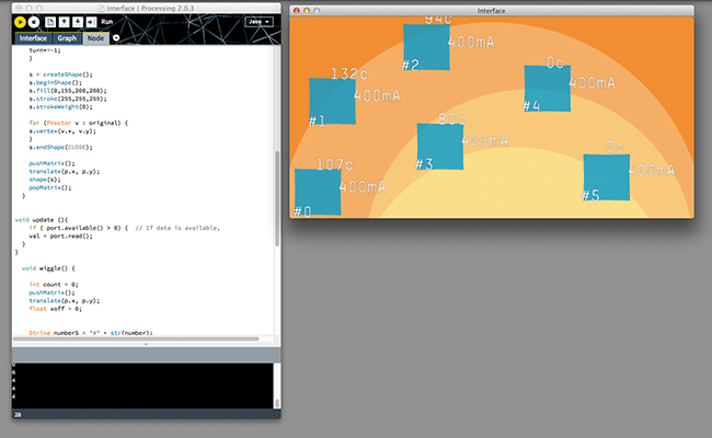
Interface and Application Programming
Assignment Thirteen
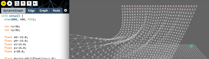
Back in week 10 I had a lot of fun designing interfaces for the step response sensor. Since both interfaces, shown in the video above, explored serial connections to input devices and graphic read outs, I thought it would be a good idea to start work on my final project interface which was going to have a few extra layers of object based programming for agent modelling.