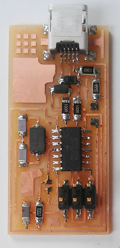
![[Image_Missing]](img/projects/week-02a.jpg)
This is the final board. The first one I have ever soldered.
![[Image_Missing]](img/projects/week-02m.png)
I used this inner trace that I found on the class website.
![[Image_Missing]](img/projects/week-02n.png)
I used this outer trace. The two trace images have been scaled to be equally wide on the website (for aesthetic reasons), and should probably therefore not be used to mill any board. The traces with the proper proportions can be found on the class website.
![[Image_Missing]](img/projects/week-02b.jpg)
Since the tolerances we were working with were so small (0.1mm), and since the bed of the machine is not flat, a sacrificial layer was added to the bed, with a flat section milled out to ensure a planar working surface.
![[Image_Missing]](img/projects/week-02c.jpg)
Milling the PCB board. Good to remember that only non-reinforced boards should be milled to avoid wearing out the tool prematurely. Also, some suggested that when inserting the tool, one should leave it loose, and adjust the z-height to the proper setting and then tighten . However, as one adjusts the z-position, the tool spins while one holds the loose tool tip (and I was worried of injuring my fingers ). I later was told by my lab-mate, that he usually tightens the tool lightly with the tool almost completely inside the milling head (so that he doesn't have to hold it), then adjust it to the correct z-height, loosen the tool, and adjust the tool tip to the correct position. This method sounds far superior to me, and I will be using this workflow in the future.
![[Image_Missing]](img/projects/week-02d.jpg)
The completely milled inner sections of the board. Only minor deburring required. Since it passed the inspection, the next thing to do was to mill the exterior.
![[Image_Missing]](img/projects/week-02e.jpg)
After milling the outer path, the board was ready to be removed from the bed. I removed the excess outer part first, to get better access to the board itself, and to be able to lift it at less of an angle (to avoid chipping the board).
![[Image_Missing]](img/projects/week-02o.png)
The image of the traces and components that we were to use. As I have no experience with electronics, most of these did not mean anything to me. Luckily, I received some help from other students in my group, and was able to figure out what the different abbreviations meant.
![[Image_Missing]](img/projects/week-02f.jpg)
The parts were much smaller and more nondescript than I had realized. (Loosing them or mixing them up would be a concern.) One of the students in my group had taped the parts onto a piece of paper with double-stick tape, which I thought was a great idea. Since I didn't want to ruin the pages in my notebook, I decided to simply draw placements for the different parts, and be extra careful not to bump my notebook. In the end it worked out well, and it was definitely a good idea to find all the components first. It was easily to keep track of how many components still needed to go on the board, and gave some reassurance that I had not forgotten any when the list was empty.
![[Image_Missing]](img/projects/week-02g.jpg)
I found the light and magnifying glass very helpful, although no one else seemed to appreciate it, and didn't want anything to do with it. I was worried my hands would be too shaky, but it didn't end up being a problem. Clamping the board in the vice also helped, as I was able to rest / steady my hands agains the vice when soldering. (Also, as an added bonus, the large magnifying glass also seemed to deflect some of the fumes and prevented me from inhaling the most condense puffs of smoke.) I tried to remember what we had been taught. Check that the tip of the iron is clean and has a thin layer of smooth solder on it. Heat the copper and the solder. Not just one or the other. Heat it for a bit before applying the solder. Don't remove the heat immediately. Put down some solder, then the component, and reheat the solder. Then do the other connectors, and relieve tension for larger parts. Everything went well...
![[Image_Missing]](img/projects/week-02h.jpg)
...until this happened. I was so focused on trying to make good solder joints, that I forgot to stay focused on what is important: that the connectors line up. So, I got to practice removing components. Unfortunately, we had not talked about this in class or in the tutorials yet, so I had to improvise. I first used the copper braid to suck up as much solder as possible (again, we had not talked about adding some solder to the outside of the braid to improve it's wicking abilities... this was mentioned in the class after our soldering assignment). I removed as much solder as I could, and then heated one of the corners of the USD connector, then the other, and tried to lift. By the time I got the second one melted, the first one had already re-solidified, and it was impossible to lift the component. I therefore used a pair of pliers as a makeshift crowbar (Do not do this ) and wedged the corner of the USB connector upwards as I heated the solder joint. Then I moved onto the next corner, and again, applied some pressure until I started getting the corners up a bit. I was finally able to pry loose the USB connector while using the soldering iron to heat the remaining solder. I later found out that you are supposed to grab the component you want to remove, and lift the board by it. Then, you heat the solder joints until the board falls down and you are left with the component you wanted to remove. Luckily the tweezers I had used did not bend and were fine.
![[Image_Missing]](img/projects/week-02i.jpg)
Removed and repositioned. I was very proud of the solder joints that I was able to create for the USB. We were told that the connectors are so close together that it might be difficult to solder them individually, and were therefore taught a technique where solder was applied generously to all of them, and then wicked away with the braided copper. However, I did not need to resort to that, as I got lucky and was able to solder all the connectors individually. In this picture you can also see the flux that I had applied to the board as per the recommendation of the TA's. Reading the label of the bottle, it seems somewhat nasty, and I think in the future I will try my luck without it.
![[Image_Missing]](img/projects/week-02j.jpg)
I liked how these tools looked. On the left, the flux remover, that I sprayed generously on my part. (I later realized that I should have also vigorously cleaned the board with a toothbrush or something similar, which I did not do.) After spraying the flux-remover, and waiting a while, I then also washed the board with water.
![[Image_Missing]](img/projects/week-02k.jpg)
Having not done anything with electronics before, I cannot tell you how wrong this felt. Apparently it is completely OK to do, as long as the electronics are not powered up.
![[Image_Missing]](img/projects/week-02l.jpg)
After my board was complete and cleaned, I used my lab-mate's FabISP from last year, and Anna Kaziunas instructions to program my own FabISP. It took two tries, but then it worked. I have no idea why it didn't work the first time, which would have been nice to know.