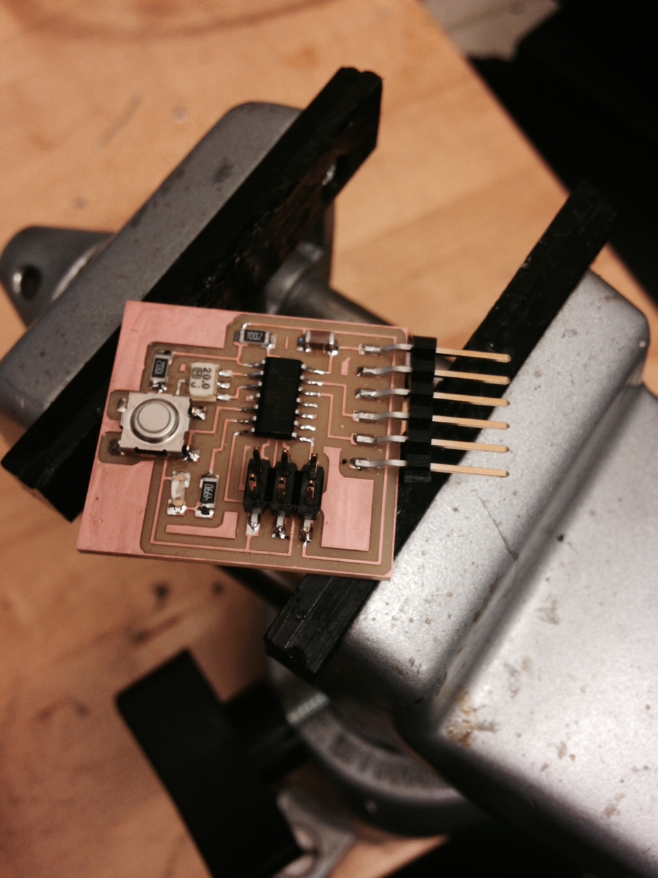
This week's assignment was to redraw the echo hello-world board using Eagle and then fabricate it. I also had to add a button and an LED to the circuit. It all went pretty well except for some shortcomings with the fab module that made milling the board a headache.
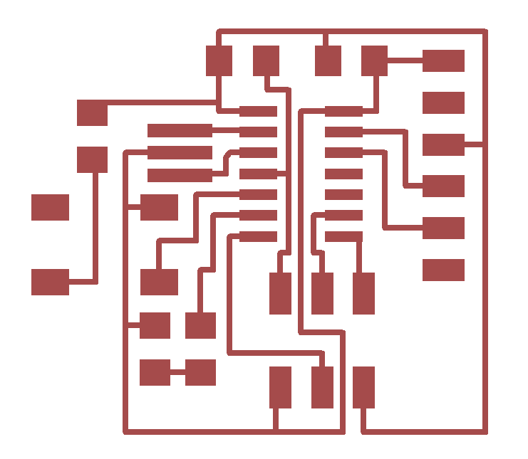
The first step was to design the circuit in Eagle. I created a project and then created a schematic within the project. I used the fab.lbr file provided to add common fab lab components to my Eagle library. I basically just followed the picture of the traces provided above to determine which components needed to be connected to each other. To add a button to the circuit, I used the 6mm Omron switch and connected it between an unused pin on the microcontroller and ground with the pin being pulled by VCC through a 10k Ohm resistor (see schematic below). This makes it so that when the button is not pressed, the pin is guaranteed to be at VCC. When the button is pressed, it drops the pin to ground. To add the LED, I connected it to another unused pin, a 500 Ohm current-limiting resistor, and then to ground, making sure that the cathode of the LED is towards ground. This makes it so that when the pin is activated, current will flow through the LED and resistor and to ground and the LED will light up. Because I didn't have the most updated version of the library, there was no component available for the LED. But knowing that the LED and resistors have the same footprint, I added it as a resistor, named it LED, and made special note to myself to remember that the component is directional

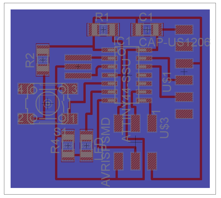
The next step was to create the traces. I created a board from the schematic by clicking the "Generate/switch to board" button. Again, I followed the example board provided to plan my traces and copied it as precisely as I could. I set the grid to 10 mil (to ease in finding the centers of some components) and made sure that there was always about two grids between traces (16 mil is the minimum distance for a 1/64 endmill).
Next I made a box around the traces and shrunk the workspace around the box, each with 40 mil clearance. This allowed me to export a png with only the bottom layer visiblie in order to create the profile cut. I exported one png for the profile cut and one for the traces (adjusting layer visibility each time) using the settings monochrome and 500 dpi.
The rest of the fabrication was exactly the same as for the FabISP In-Circuit Programmer (load pictures into the fab module, send to Modela, 1/64 mill for traces, 1/32 mill for profile, clean, flux, solder, remove flux). I spent a couple of hours banging my head against the wall trying to get the fab module to communicate with the Modela because apparently the module had been changed and was not left in working order. I have zero interest in explaining how to get the fab module to work correctly -- that's Neil's business and I don't consider "learning how to use the fab module" an important skill since nobody else in the world uses the fab module outside of fab labs. Anyway, once the TA's sorted that out, I milled and stuffed my board with no problem.