After my Charlieplexing failure, I had to recover quickly for the Output's week and continue
with the Networks week. Thus I decided to make a board that will have both outputs and networking
and even more ! The choreographer of this architecture will be an ATMEGA32-U4 and I will try to
make full use of it's 44 pins!
I will use a 20MHz crystal, which will provide plenty of time to do the embedded
software communication for all the modules. An iteration of this board will be used
as an output module for my final project. This will be possible via the slave header, which
will be used to implement SPI (Tx,Rx).
First Try
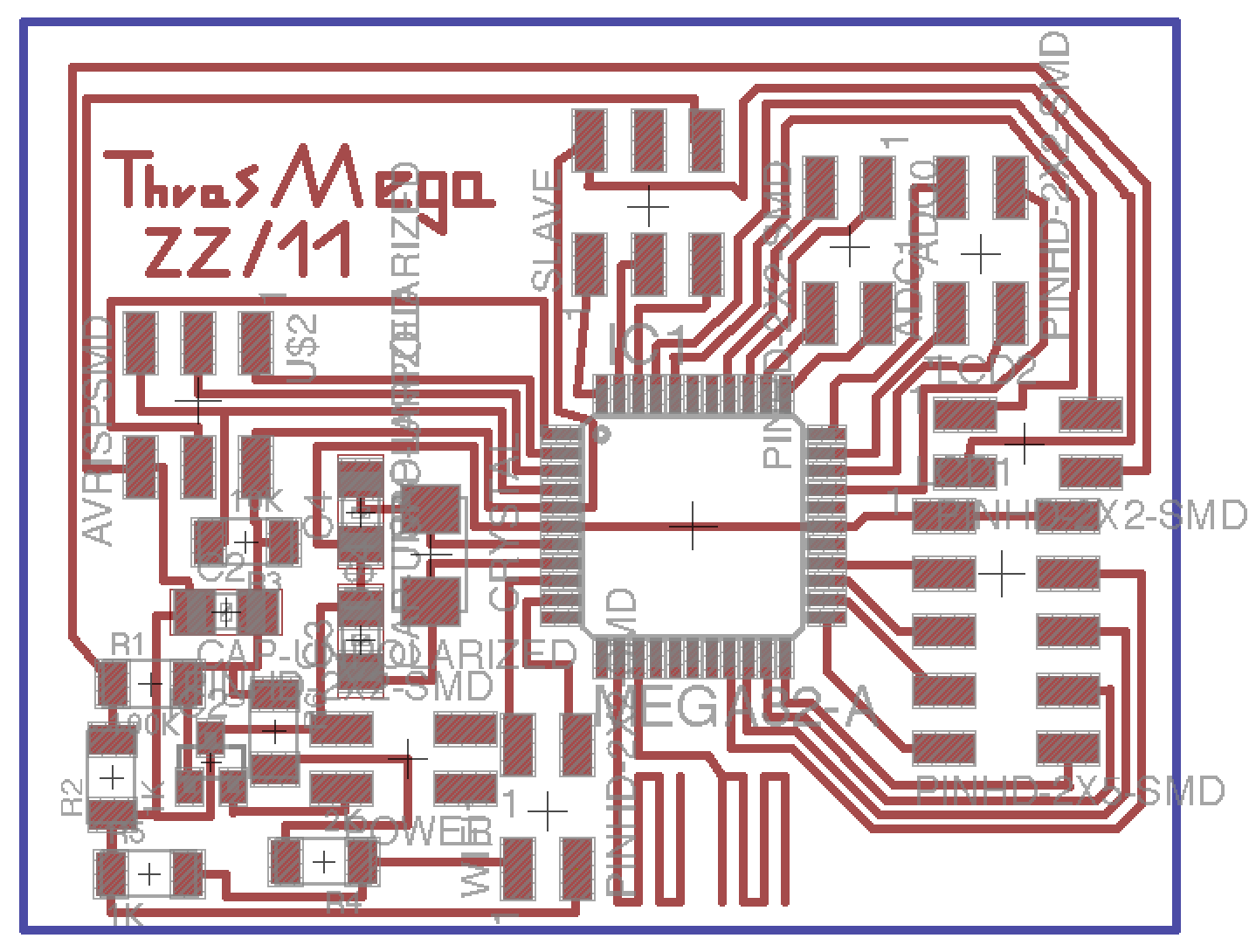
On the right you can see my inital approach for the module. It includes the following:
-ATMEGA32-U4
-20MHz Crystal and its capacitors
-5V 0.1 Amps LDO Regulator and capacitors for smoothing
-headers for 16x2 LCD screen (LUMEX)
-voltage divider and headers for ESP8266 WIFI module
-headers for a slave module (5V VCC)
-headers for an 8-bit port (ADC pins)
My main concern was to have the LCD and the WIFI module, so that I can later on use this
board as an output module for my final project (slave module). Yet, I put a header for
the last port (ADC port) too, in order to test the 1MSPS ADC of the processor.
The routing for this board initially was a challenge , as I was using 16mil traces. Yet,
when I switched to 10mil traces, I could move freely around the smd pads and the routing
was straightforward. I run a design rule for both 16mil and 10 mil clearances, in order
to minimize the places where the 10mil endmill had to be used.
While designing the board,
I took advantage of two empty pins and made a patter for a capacitive button. It's worth noting
that during the design I have the grid on, in the size of the traces with an alt of 1mil for
best alignement. This setup makes it a lot easier to route between pads while watching out
for clearances.
The milling process was problem-less this time. I ran the whole file with the 1/64 inch endmill which
cleared happily most of the board. Then I used the 10mil endmill for the microcontroller pads and
the tightly packed traces. A posteriori, I think that it is better to have bigger than 10mil traces, as
it is really easy to accidentaly peel off a trace with the tweezers while aligning an smd for soldering.
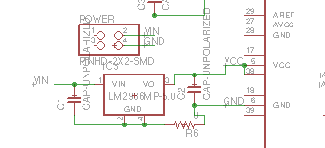
Prior to connecting the LCD and WIFI modules, I wanted to check that the voltage regulator worked fine
and that I could see the board from my programmer. Yet, for some reason the voltage regulator had
a constant output of 2V for an input of a 9V batter! I soldered a new regulator and again the output was 2V, even with
a 20V input from a lab bench power supply. To make matters worse,
I tested the regulators alone and they both worked fine, so for some reason my board had a problem.
Given the fact that I had also forgotten to provide a pinout for the CH_PD pin of the WIFI module,
I didn't spend more time on this board and decided to design a new one. I will, though, return to this problem
because it is really weird that the output voltage drops that much even with such a small load in the output.
Second try
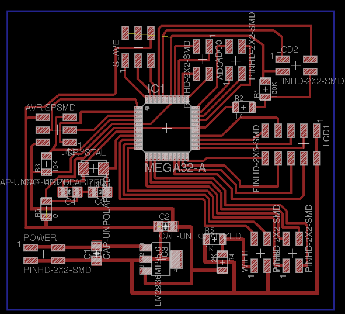
The schematic remained the same for the most part of it, now with all the pins of the WIFI
module connected to portA of the microcontroller. This time I went with the 5V 1A regulator,
which is a more sane choice since when all the modules are powered the current drawn will be
a lot more than the 0.1Amps of the LDO regulator I had before.
Note that the WIFI module works on 3.3V , so I still used a voltage divider to power it. Here is a
nice website I found while googling
in a rush "voltage diveder calculator". This calculation is trivial but it has many more little calculators
written in javascript that can be handy sometimes. It was a nice bookmark.
In this iteration I went with 12mil traces instead of 10mil to play it safe. I also made
the traces around the regulator bigger for better heat distribution in case the current
gets high enough.
The milling process was again straightforward but at some points, when the 10mil endmill went through the traces that
were already milled by the 1/64inch, it milled them even more, resulting to some super-thin traces (see image below).
I guess that's because the 10mil toolpath is slightly shifted upwards from the 1/64inch as the offset is from the edge
(black vs white) to the circumference of the endmill, not it's center.
(Drag) Soldering!
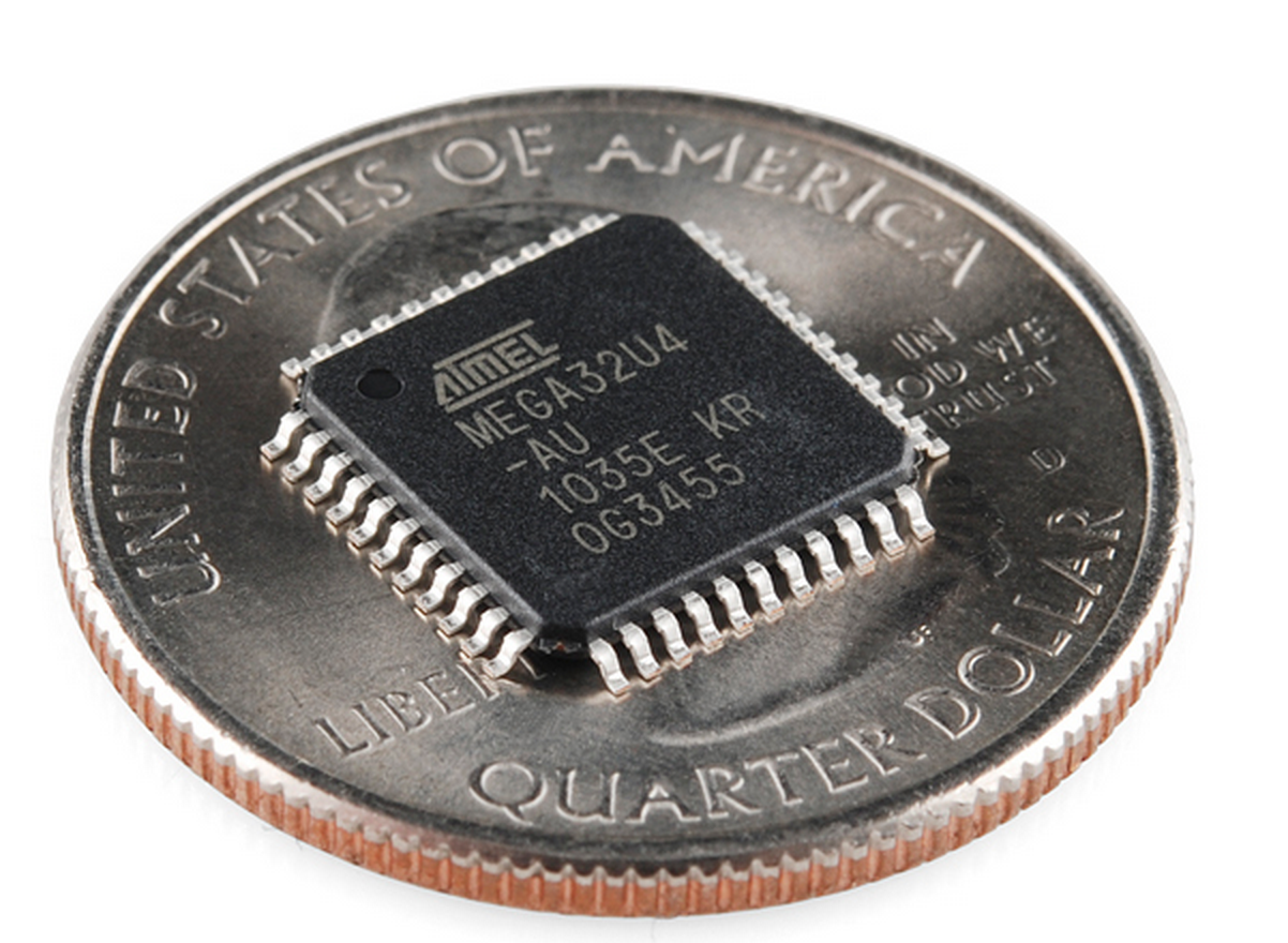
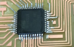
This week I had to solder the ATMEGA32-U4 package, which has 44 pins. While the pin size is still
big enough to solder every pin at once, it was time for me to update my soldering skills. I had the
option of either using soldering paste and then the heatgun , or the coolest thing ever: drag soldering!!
Drag soldering is a technique where you apply a "huge" blob of solder and slide it through the pins. In the end the solder
stays only on each pin and the correspoding pad, due to heat distribution.
As a warmup, I watched this video. Note that
to drag solder you have to use a big soldering tip so that you can distribute heat evenly while dragging. It turned out
to be an easy but very effective process to solder SMDs with many pins and I was very satisfied with my first try :)
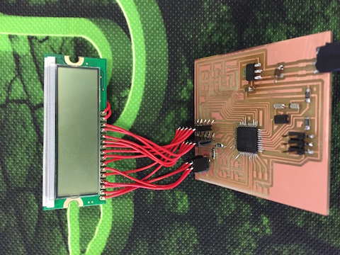
Programming the LCD screen
The LCD screen works!
For details on programming go to my outputs page (week11).
Programming the Wifi-module
OK. Now here is the real deal for this week: communicating with the ESP8266 module. To communicate
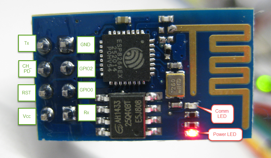
I will use the hardware serial of ATMEGA32 (pins TXD,RXD). Here is the pinout:
-VCC: typical voltage is 3.3V for ESP8266, with up to 240mA consumed. I am feeding ~3.5V with the voltage divider.
-RST: connected to pin PD3, active low, pull up for normal operation
-CH_PD: connected to pin PD4, pull-up needed for chip enable
-GPIO0: connected to PD5 pull low for updating firmware via UART, it looks like it can be left floating in normal operation,
-GPIO2: connected to PD2 unused by current official firmware; modified firmware from electrodragon.com allows controlling both GPIO0 and GPIO2 with either AT commands or commands sent via TCP/UDP,
-TXD, RXD: UART, connected to TXD,RXD pins of ATMEGA32.
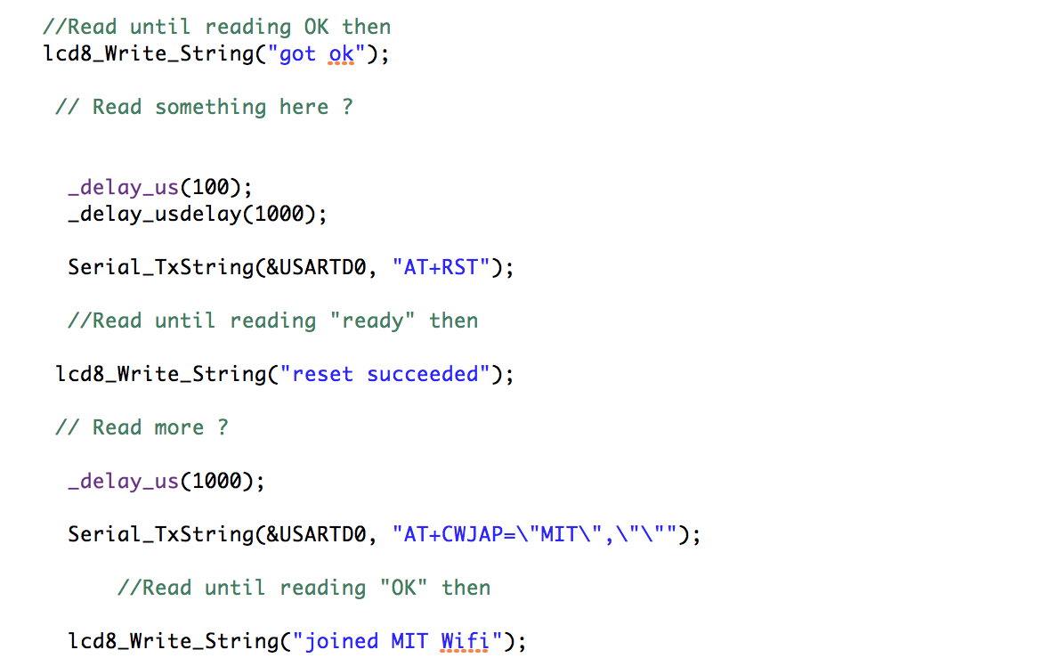
The ESP8266 wifi module uses AT commands to function (like the ones in old modems). There are four different ways you can send
a command depending on whether you want to :
-Set the value of a variable : AT+=<…>
-Find the value of a variable: AT+?
-Test a variable with a value: AT+=?
- Execute an operationg command: AT+
After playing a while with the Wifi module connected through an FTDI cable and communicating through Arduino Uno serial interface,
I was ready to write the commands which the microcontroller has to send to connecto to the Internet. The implementation was straightforward
and the wifi module was happy to connect to the MIT Network. In the next iteration of this board I will have the Wifi module
sending data to my web application, which I learned can be done in two ways:
either have the ESP8266 act as a webserver and send get requests, or have the module as a client and feed the data through a websocket.