Building FabISP with a pre-defined pattern is less creative but an essential step to build 'brains' for future projects.
Aha moments
- Neil coded minimal viable drivers for milling machines by himself to adopt to newer operation systems.
- Debugging hardware requires more structured approach than software and takes time.
- Solder flows to where it is comfortable. It makes even a tiny pin attached to a tiny tip nicely.
- The circuit boards and components sitting there started to be a bit more familar to me. I did not have the sense when I dropped my smartphone in water and dissected it to dry a half year ago.
Build FabISP
FabISP is a fab-able in-system programmer. It allows us to program the AVR microcontrollers on other board we make in the future. AVR microcontroller is manufactured by Atmel. This board also uses ATtiny44, one of the AVR family.
There are two types of major microcontrollers: PIC and AVR. We use AVR for this class.
Chip components (resistors, diodes, capacitors, crystals) look completely different from traditional components.
Designing (0:00)
I used the template without designing the circuit by myslef this time.
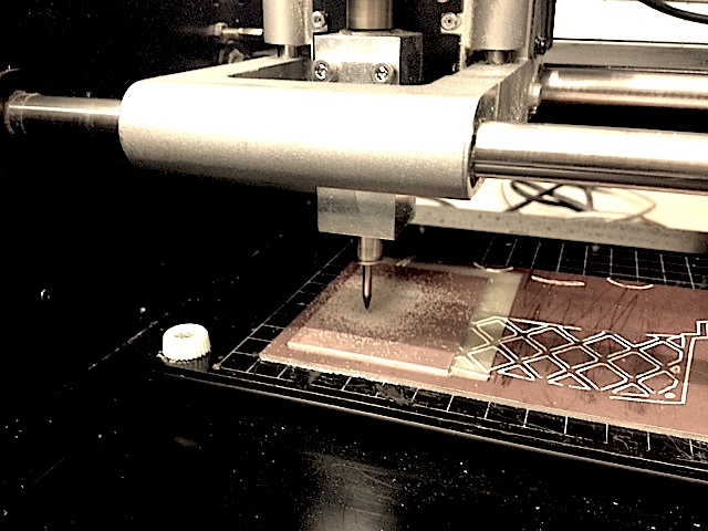
Milling and soldering (2:00)
Milling out the board and attach proper components on it. I referred to Jeff's tutorial.
- Milling the PCB board
- Load the image file
- Zeroing
- Mill the circuits with a 1/64 inch end mill
- Change the end mill
- Mill the frame with a 1/32 inch end mill
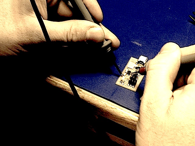
- Soldering the componets onto the board
- Fix the board
- Set the ?? 720 degree
- Put flux on the board
- Pick up and solder the components
- Remove the flux

Programming
Writing codes on to the microcontroller. Jeff offerred the equipments needed and helped me to figure out how to proceed along his tutorial. We used:
- Windows PC x 2
- USB cable x 2
- another Fab ISP with the program already embeded in it
- 2x3 pin straight cable
Debugging (0:50)
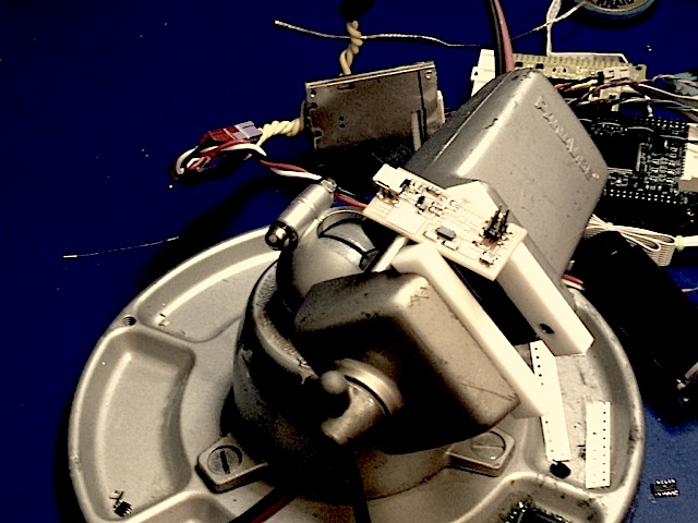
Composing the board is not so straight forward as programming is not. There also are logical steps of debugging it given certain possibility of each defect just as we debug codes. We should be aware of obstacles typical to physical settings (take more time, need multiple steps to remove something).
- Removed flux with alcohol brushing with tooth brush
- Checked appearance of the board
- Compared JF’s board and my board to make sure that every components are installed correctly.
- Reworked all the solder joints to make sure that they were good
- Changed the power source from USB to the other board (by changing the jumper)
- Using two USB ports, one for the data and power and one for just power, may cause unexpected results. Just wanted to get rid of the possibility that the computer is confused by two USB connections.
- Checked the metrics for components with a tester
- Tested diodes, resistors, and capacitors whether to indicate proper values.
- Conducted short-circuit tests on the board
- Tested that each lines work fine and have no abnormal short circuits.
- Conducted short-circuit tests between connectors
- Tested the connectors and the six lines which connect two boards work fine.
- Replaced the IC on the board
- ICs sometimes crash by heat or have initial defects.
- Replaced the capacitors on the board
- Capacitors which allocated for a crystal have not so much allowance. Used the same lot as JF’s which worked fine. Since we couldn't measure values as low as 10pF and because the 100pF are visually the same we removed them and installed fresh ones.
- Replaced the crystal on the board and then worked
- Crystals sometimes crash by heat or have initial defects. Used the same lot as JF’s which worked fine.
(Re-)Programming (0:05)
Then it worked fine!