Desigining
Schematic Design

Installed Eagle to my laptop. Loaded the fab class lib file. I learned about commands of net/ label/ name/ move/ group/ show/ board as essentials. Eagle sometimes behaves inconsistently. When I placed the parts and connected lines to each end of parts, it sometimes did not reflected the connection on the board view. Charles taught me several options: relaunch eagle and make sure you open both board and schematic design when you make some changes. Putting the dots on the connections between lines and components.
Board Design
 Show VCC.
 Show GND.
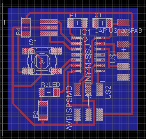
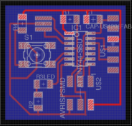
It took unexpectedly long time to design the borad properly. Want to know 'design patterns' for electronic circuits. Autorouting did not work. I placed each wiring by hand. Pressing Alt and grid guideline by 16 mil. helped a lot to avoid gaps less than 16 mil. the milling tool size.
Milling

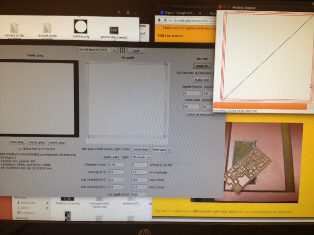


When milling the circuit, I changed z to .65. When cutting out the board, I changed offsets from 1 to 3, and cut depth from .6 to .65 to make sure it cut through. The circuit lines might have been too thin.
Soldering
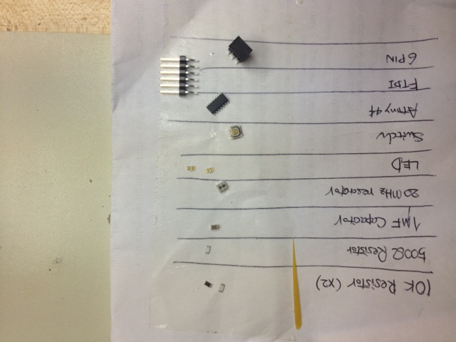
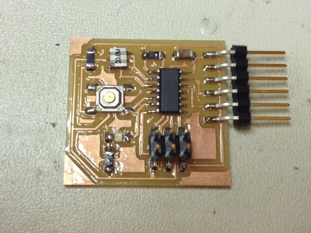
I used blue led and 500 ohm for the led resistor.