How to Make (Almost) Anything
Project 06
Electronics Design
Input
Parameters: PCB Design, Computer-controlled Milling, Soldering components
Tool: Modela
Programs: Eagle, Fab Modules
Output
This project explores how to design an object suitable to be machine-milled first, then to mold it and cast the final version.
Process
Installing Eagle, The Fab Library, The Fab dru file to run the error check before exporting the images.
Reading the Sparkfun tutorials .
Looking at former students' various designs.
The design process requires many detailed steps and back and forth between the 2 windows. They must be kept both open constantly.
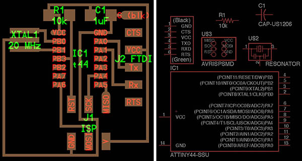
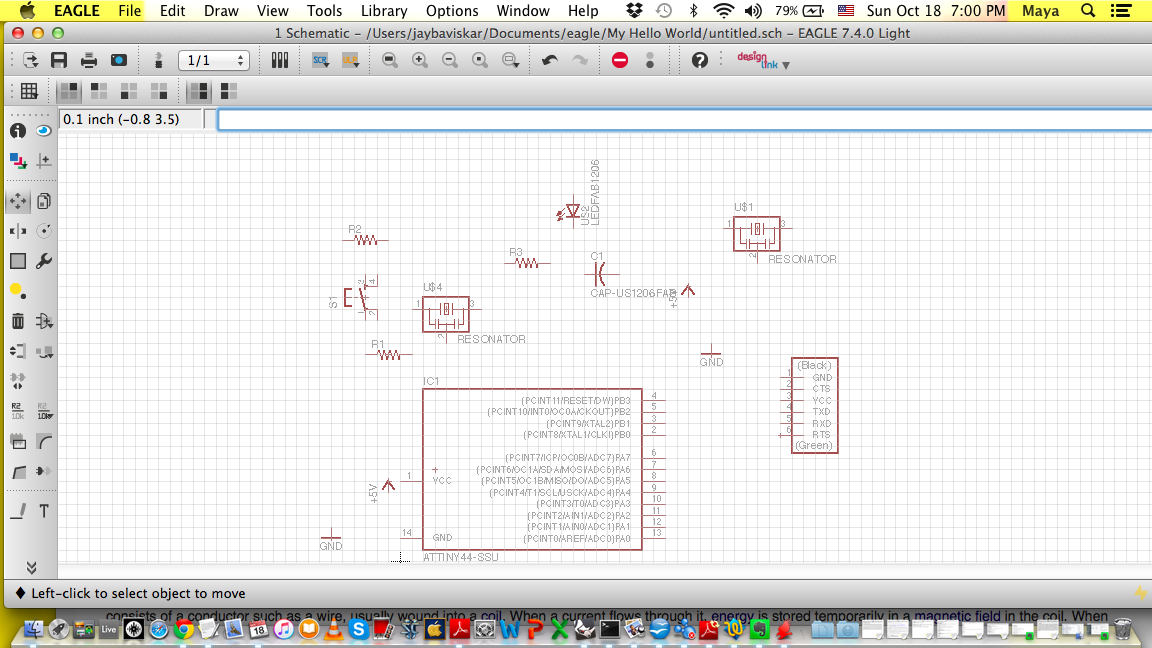
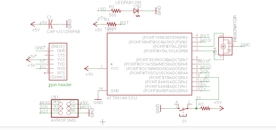
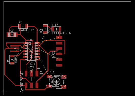
1. In the Schematic window: start by finding and importing the right components from the library. Wiring them with the "NET" wire or using names and labels to connect them. Calculating values for resistors using Ohm's Law.
Diodes: look for Voltage drop in data sheet, look for DC forward current 40mA in Absolute Maximum Ratings. So let’s take 30mA or 20ma.
Forward voltage drop VF 1.8V if IF=20mA (5V= 1.8 (voltage drop LED) +3.2 (voltage drop resistor)
V=IR So 3.2=(0.020)R So R= 160Ohms
Run ERC to check for erros, mis labeling and lacking values
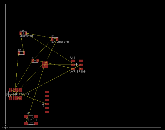
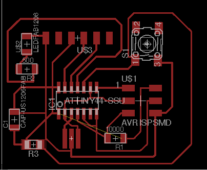
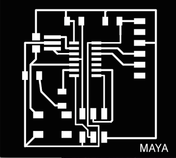
2. In the Board window, place components as relevantly as possible, respecting their orientation (diodes, micro controller) rotating them, hitting the ratsnet command each time. There is a margin of error in Eagle's routing understanding but it leaves freedom for design. I didn't try the Autorouting knowing the issues of a lack of preliminary protocol.
Remember to adjust the grid, use the -Alt key for finer grid control when routing. Run DRC and load fab.dru file to check for errors. In case of unsolved routing, using jumpers/O ohms resistors is possible but so... inelegant.
Test A: error: wishful thinking. Like in any good mind game, remember Rubik's cube, the unsolved parts will not resolve at the end. On the opposite, they all add up and I resignedly exported a first version requiring 4 jumpers!
Test B: asset: stubborn sense of style. I rechecked my Schematics to see if there were any possible improvements but it was matching former students' schematics >or
I couldn't modify the order of the 6 pins because of using a different component from the start. Wonderful patient help from TA Sam Calisch
Test C: motivation: being pointed at the sufficient space in Neil Gershenfeld's original, I opted to start from routing the same VCC and GRD routing and an identical orientation of the shared components. Moment of illumination followed. All the puzzle pieces fit. 0 jumpers. I used R3 to route my wire under. 0.012 width to run between the micro controller pins.
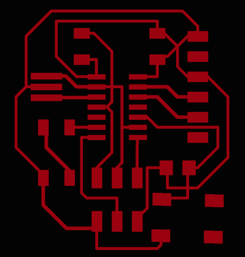
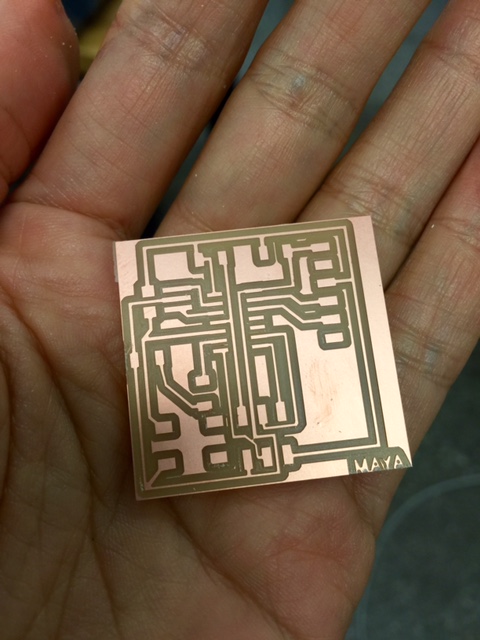
Exporting the images to mill the board: First choose the corresponding layers. Layer 1, Monochrome, 600dpi. For the outline, layer 40, draw a rectangle inside the outline, monochrome.
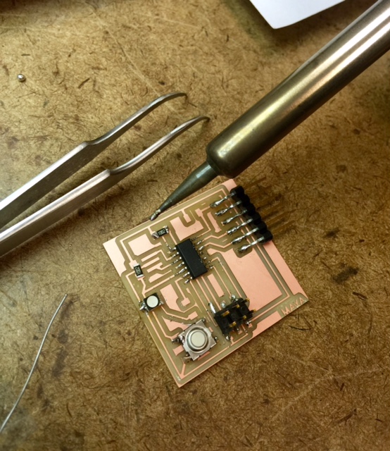
Soldering and Assembly: Been there, done that. No major error. Putting a drop of solder on the wick to absorb any excess or misplaced solder.Proceeding from the 6 pins header on the boarder. Respected the direction of microcontroller and diodes. A little less small victory.
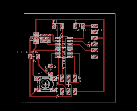
Board components: mini USB connector; resistors (4): 10k(x2), 499ohm(x2); capacitors (1): 1 uf; resonator: 20 mhz; IC1 microcontroller: attiny44a; conector: j1 isp 2x3; 6-pin programming header; LED: (blue) clear 1206 3.3V 20mA; button: switch tactile SPST-NO 0.05A 24V; single sided circuit copper board stock: 1.6”x1.6”