Week 2: Electronics Production
FabISP In-Circuit Programmer
September 24, 2015
Even though I was an electrical engineering (and computer science) major in college, I never learned how to actually design and print my own circuit boards, so I was pretty excited for this week's project. Also, one of my labmates took HTM(a)A last year and often speaks about how useful it is to know how to make PCBs. I thought I'd jump right in by making the hello.ISP.44.cad board (the first board design on the assignments page). For the traces, I used the 1/64" setting on the Roland Mill with a depth of .12 mm, speed of 4, and offset of 5. On my first attempt, the piece of stock wasn't held down tightly enough, so the mill forced it loose and it shifted. I cancelled the job and repositioned the stock with more tape, and pushed it down more securely. This time, the piece stuck and I was able to print the traces.
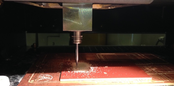
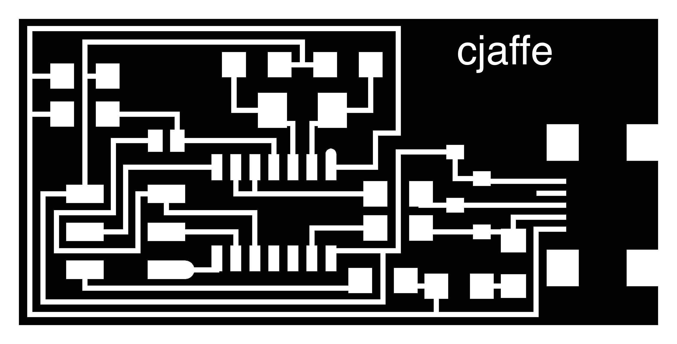
After the traces finished printing, I switched out the 1/64" endmill for the 1/32" endmill and loaded the board design into fab modules. I used the default settings that loaded into fab modules and used the xmin and ymin that were saved from the previous job. Unfortunately, when I started the job, the endmill almost immediately dislodged my piece from the platform again. Luckily, though, I was able to stop the job very quickly, before my traces were damaged. I pulled up the stock piece, cleaned the platform and repositioned the piece again, this time placing it even more firmly and pressing it down very hard. I very carefully positioned the endmill head, just judging xmin and ymin visually. I also set zmin manually using the standard process. This time, when I hit send, it worked! You can tell the "board" cut is slightly offset from the traces because there is a little extra copper around the edge of my board, but I don't think it will affect the functionality of my circuit. Other than that, the traces came out really cleanly, and didn't require much cleaning or deburring. I will plan to tackle soldering sometime this weekend, and perhaps experiment with a few other board designs (or a flexible circuit)!
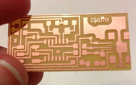
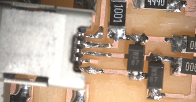
This afternoon I went to the basement lab to stuff the board. It took me a lot longer than expected. I thought it would take me about an hour to do everything, but from start to finish (gathering the parts, soldering them, having to remove them using the copper braid and resoldering them), it took me about 2 hours of careful, patient work. Even though I've soldered before, I have never soldered such small joints! The larger components (resistors, capacitors, etc) were do-able, and I got better at doing them over the course of the 2 hours. I had a lot of trouble with the tiny leads on the ATTiny44 and the USB connector. I learned how to use the copper braid out of necessity so that I could remove and resolder the joints for those components several times. Eventually, I got all the components on there. It's not pretty, but they're all there. I used the multimeter to check that voltage and ground aren't shorted, and tomorrow I will attempt to program my board and do more testing!
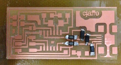
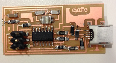
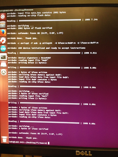
As I have learned is common in this class, "testing and programming" did not go as smoothly as I originally planned. When I first went to the lab, I checked that voltage and ground weren't shorted and that the correct voltage (~5V) was showing across those pins. I tried to upload code to my board but kept getting a "bad AVRISPmkII connection status" error, even though the board was powered and the USB pins connected in the right way. Jonathan Bobrow looked at my board and noticed that I was using a 20MHz resonator instead of a crystal, so I went back to the lab and switched out that component. Then, Eric VanWyk looked at my board with me under a microscope, and noticed that several of the leads on the ATTiny were not connected! Eric also helped me take some awesome pictures of my board under a microscope. In general, the feedback I got on my soldering joints was that they were a bit lumpy; next time I will try to heat up the copper more so that the solder "wets" the joint more. Will Langford helped me fix the ATTiny connections, and once I felt reasonably satisfied with my board, I tried to program it again. Finally, my board worked! I programmed the board using the computer in the downstairs lab, which already had avrdude and the proper compilers. The "programming" sequence is:
- make clean
- make hex
- sudo make fuse
- sudo make program
If it works, the terminal output of "sudo make program" will show that it is "Reading" and "Writing" and enumerate a bunch of processes. If there is an error, avrdude will let you know in the command line output. After I verified that I had programmed my board correctly, I desoldered the two "jumper cables" (I used 0 ohm resistors for these) and made the IDC ISP cable. Will helped me use my newly minted FabISP board to program another board with the hello.button.44 test program, which was successful!
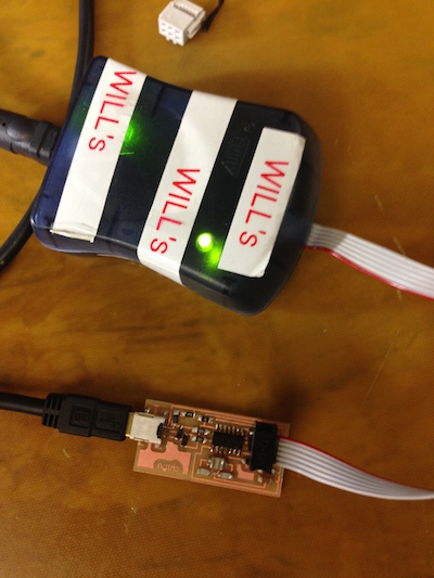
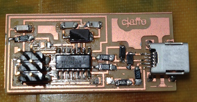
Concluding thoughts and thank yous: This week took a lot of patience and attention to detail. One of the ideas that was drilled in, through the process of trying to figure out what was wrong with my board, is that hardware is hard to debug because there are so many parts that must come together for the final product: the board, the components, the soldering, the programming setup, the embedded software. I am very grateful to Jonathan, Eric and Will for sharing their expertise and helping me identify and fix problems with my board. I also found Jonathan's FabISP tutorial very useful for troubleshooting the board programming. I had some more ambitious ideas about using the vinyl cutter to print my circuit traces or making a flexible circuit, but those will have to wait until a later date...