Electronics Design
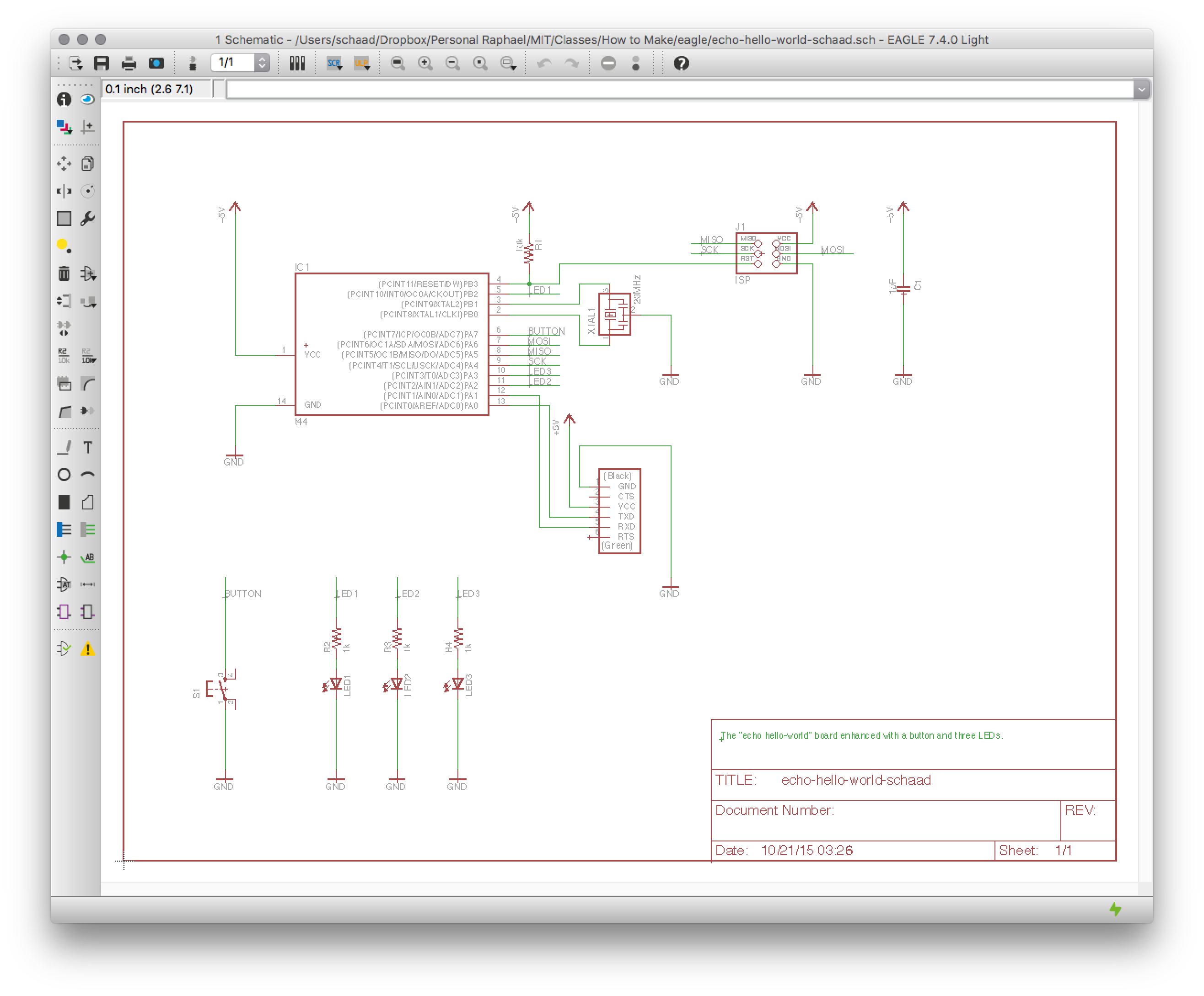
Enhanced "echo hello-world" Board
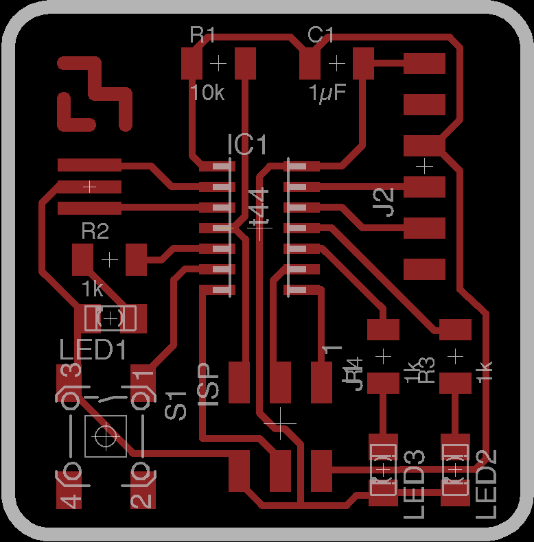
To learn more about the toolchain that comes before fabricating PCBs (see Week 3: Electronics Production) we redesign the “echo hello-world” schematic, and enhance it by adding a light-emitting diode (LED) with a series resistor and a switch to two empty pins of the MCU. From that we create a board layout and use the familar process – or a new one – to fabricate it.
For our projects, the electronics design workflow is generally a two-step process:
- Designing circuit in schematic editor, optionaly simulating with capable tool
- Component placement in board layout editor and route traces, manually or with autorouter
After that, fabriation begins. For these two design steps for our projects EAGLE is a recommended software. Downloading the full version and after installing clicking the “Run as freeware” button will give us all we need. There's a three great tutorials on EAGLE from sparkfun: Install and Setup, Schematic, and Board Layout
.Use the “Net” tool (green lines) to connect components. To avoid a mess of wires, use the “Label” tool (green wire) in conjunction with the “Name" tool to create invisible connection between net stubs. Check the connection with the “Show” tool.
In addition to choosing commands from menus and icon panels, there’s a “command line” interface in EAGLE. Some favorite commands I’ve used often (Cheat Sheet):
- General: rotate, move, info
- Schematic: add, show, net, delete, label, name, value
- Layout: route, ripup
// Hardware: // Based on Neil Gershenfeld's board: http://academy.cba.mit.edu/classes/embedded_programming/index.html#echo // With my redesign and enhancements: http://fab.cba.mit.edu/classes/863.15/section.CBA/people/Schaad/week6-electronics-design.html #define LED1 (1 << PB2) // red (pin 5) #define LED2 (1 << PA2) // green (pin 11) #define LED3 (1 << PA3) // green (pin 10) #define BTN1 (1 << PA7) // (pin 6)
- supply1/+5V
- supply1/gnd
- fab/attiny44-ssu
- fab/resonator
- fab/res-us1206fab
- fab/cap-unpolarizedfab
- fab/avrispsmd
- fab/ftdi-smd-header
- fab/6mm_switch6mm_switch
- led/ledsmt1206
It doesn't matter which free pins we use from the microcontroller. If we had a more complex circuit, the only consideration would be to avoid "using up" a pin with certain capabilities for a trivial button or LED.
I'll add this button directly without a resistor. The microcontroller already has built-in pull-up resistors on each pin, which we can enable in code. As an external resistor, we would use a high value like 10kΩ. From the datasheet I gather that the button's pins 1 & 2 and pins 3 & 4 are always connected. On press, all four pins are connected.
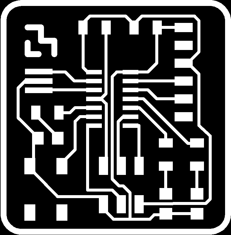
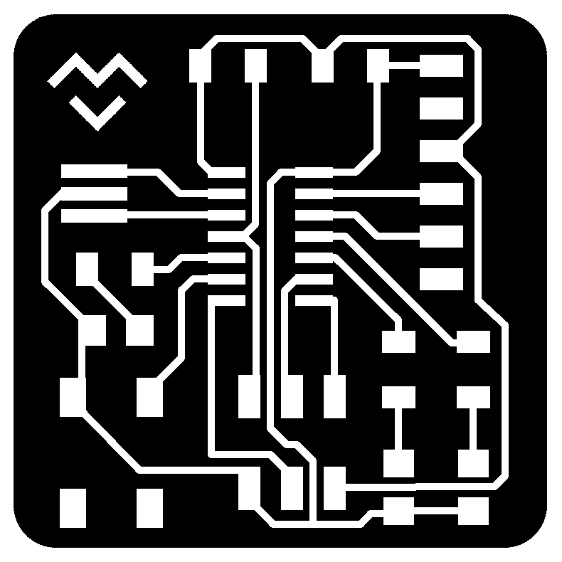
Recitation Electronics Design 101 by Jeff Duval and Palash Nandy Link to the fab.lbr and fab.dru files that are in /doc/tutorials/electronics_design and pull once in a while to see whether somebody has added new parts and push parts you design yourself. "If you want to create unique parts in a library, check out this tutorial." https://learn.sparkfun.com/tutorials/designing-pcbs-advanced-smd Add the SparFun-Eagle-Libraries: https://github.com/sparkfun/SparkFun-Eagle-Libraries V=R×I → R=V∕I Voltage (operation): 1.8V (red), 2.1V (green) Current (max): 10mA (we don't need to go constant full brightness and can operate it at ~30%) Input voltage of 5V−~2V=3V R=3V∕0.003A=1kΩ Stop mask errors during DRC happen when the layer XXX is enabled Arrange parts and refresh ratsnest until a good basic design is found Start routing Route +V and GND last- 1 Top: traces
- 19 Unrouted: yellow wires
- 20 Dimensions: outline
- 21 tPlace: some of the packages
- 23 tOrigins: center of packages
- 25 tNames: some of the labels
- 27 tValues: some of the labels
- 51 tDocu: some of the packages


you can use any drawing tools.. you are just making drawings. the best bet is to use eagle. when binarizing scanned in drawing avoid dithering with +dither option for ImageMagick. Do hand cleanup in Pixelmator.
fab.lbr from electronics_design and linked from overview page is the fab shared eagle library
    $ convert -monochrome -colors 2 in.png # Ensure the image is a 1-bit black/white PNG

    $ identify -verbose -units pixelsperinch in.png | grep Resolution # Ensure the image has a DPI of 600

    Resolution: 600x600 # If it doesn't print a line like this, then it doesn't specify a resolution at all

    $ convert -density 600 -units pixelsperinch in.jpg out.png # Set DPI to 600
convert and identify are part of ImageMagick and the code snippets I drew from my terminal-snippets.md.
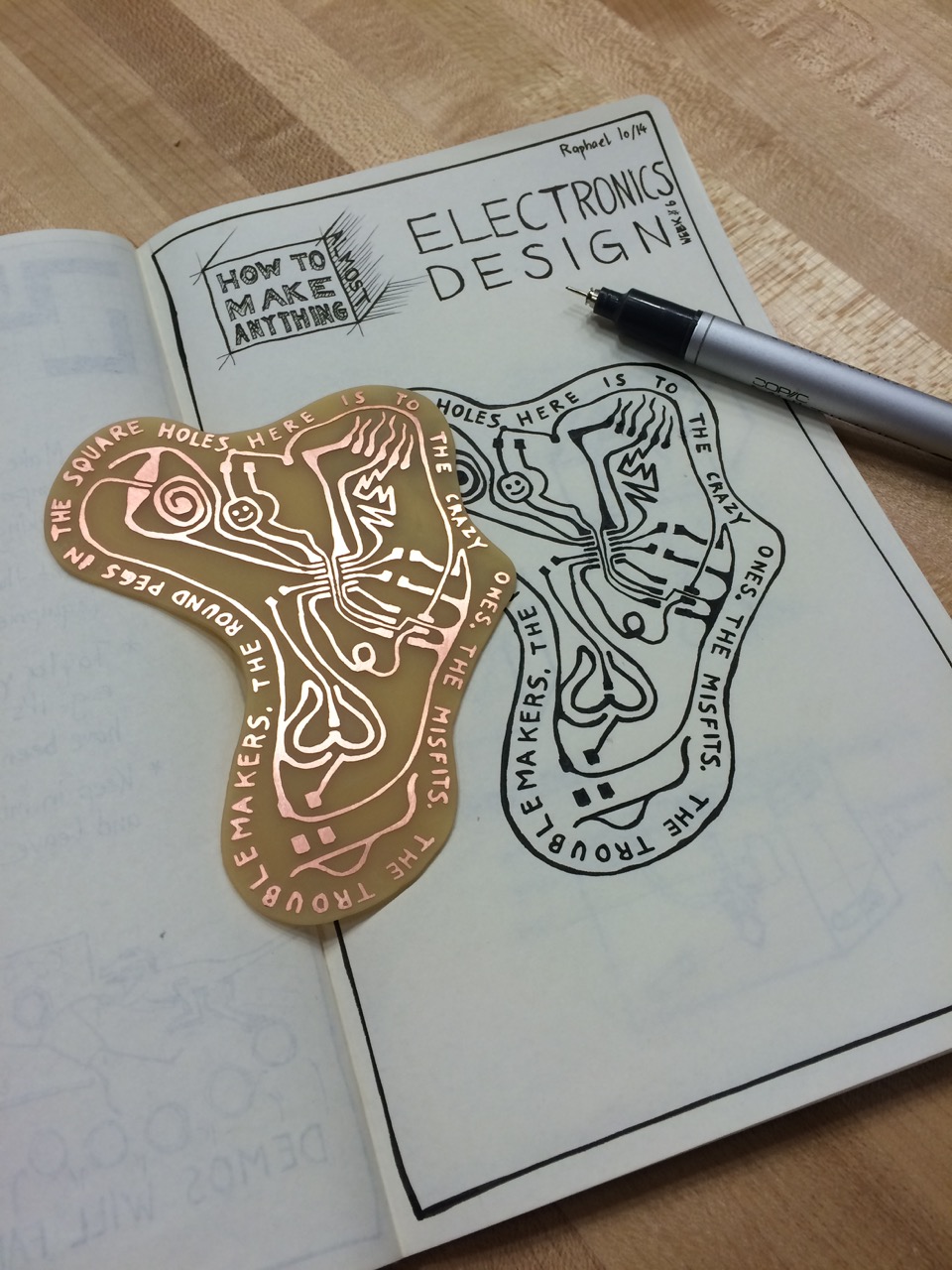
I drew it by hand. To get the pad size right, I printed the pads of the parts at 100% on paper, put it next to the notebook, and then eyeballed it.
Simulation
123D Circuits http://www.123dapp.com/circuitsOutlook
After fabricating a hand-drawn “bespoke” PCB I searched the web for other “PCB art” and was surprised to find some interesting projects. I’d like to explore this intersection more – electronics can be useful and natively beautiful.
PCB Art by Raphael on Pinterest