Demystifying the FabISP and Designing the FabOptimus
This page arose after the observation that there are plenty of resources on the web explaining how to build and program your own FabISP, but almost none which explain in detail the purpose of each component on the board, and how the board actually works. The aim of this page is to provide a comprehensive explanation about the design of the FabISP, to show where the need for each component on the board originates from, and to explain the chain of reasoning for designing a FabISP from scratch without referencing an existing design. The Prerequisites section contains resources for all of the topics you must first learn in order to fully understand the FabISP. Thus, the content is suitable for beginners, experts, and everyone in-between because the assumption is that you would begin by learning all of the prerequisite topics first.
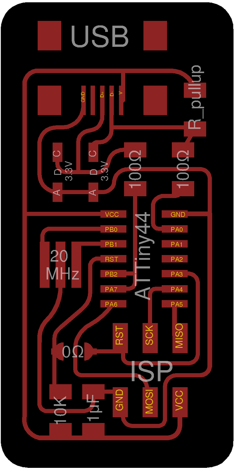
You will also find here my own version of the FabISP, which I designed as a reference board for the content on this page. The board is similar to Neil's version of the FabISP, but with a few key differences. There are no jumpers on the board other than the 0Ω resistor required for programming the board. The two series resistors (1KΩ + 499Ω) have been replaced with a single resistor R_pullup in one of the versions (more on this later). And lastly, the components and traces have been laid-out in what appears to be the most optimized way possible, that leaves no underutilized space on the board, leaves more clearance between traces, and results in a much smaller profile. Hence the name FabOptimus. (If you find or come up with a more optimal layout that does not sacrifice trace width, let me know.)

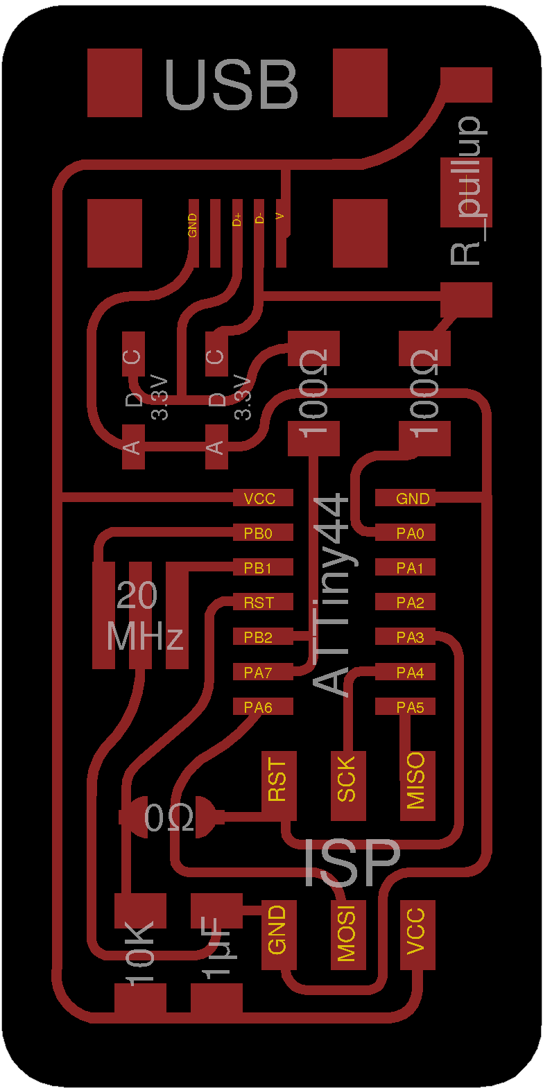
There are two versions simply because in the inventory we don't have
1.5K resistors (nor resistors whose parallel combination is 1.5K), but
we do have 1K resistors and 0.5K resistors. Thus if relying only on the
components in the inventory, you must use the version where R_pullup is
1K+0.5K. But if you have a 1.5K resistor, (or the means to create a 1.5K
equivalent resistance by stacking 2 or 3 resistors in parallel), then
you can use the version where R_pullup is 1.5K.
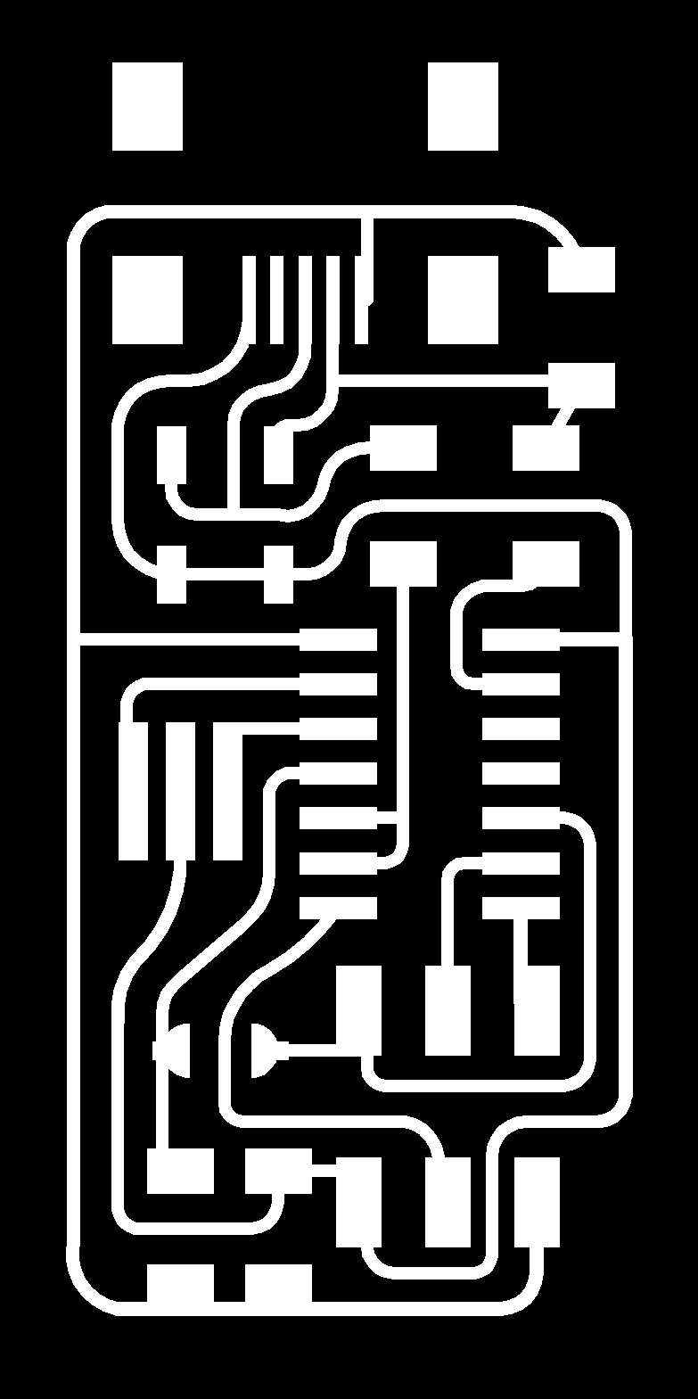
Design Files (R_pullup=1.5K): traces.png, outline.png, FabOptimus.brd, FabOptimus.sch
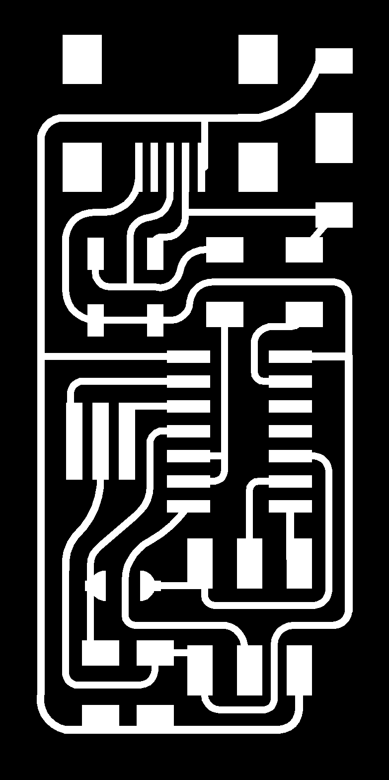
Design Files (R_pullup=1K+0.5K): traces2.png, outline2.png, FabOptimus2.brd, FabOptimus2.sch
Prerequisites
Pull-Up & Pull-Down Resistors - https://learn.sparkfun.com/tutorials/pull-up-resistors.
- Pull-up / Pull-down resistors are used for setting the voltage at an input port to V+ / GND, when no other signal is applied to that input port,
while still enabling you to change the voltage at that port by either
applying another signal to the port or by setting the port as an output.
- If you connect an input port
directly to V+ or GND without a resistor, then you lose the ability to
change the voltage at that port. If you tried changing the voltage
anyways, then a short will be created potentially damaging to the
circuit, the power source, or both.
Decoupling Capacitors - https://learn.sparkfun.com/tutorials/capacitors/application-examples
Voltage Clippers - http://www.allaboutcircuits.com/textbook/semiconductors/chpt-3/clipper-circuits/
Differential Signals - https://www.ieee.li/pdf/essay/differential_signals.pdf. ← Read this even if you are an expert. Here is another resource.
- Differential signaling uses two conductors carrying complementary signals.
- Noise that affects both conductors identically has no effect on the differential signal.
- The
inherent noise cancellation makes differential signals suitable even
for very low voltage applications, where single mode signals would be
indistinguishable from noise.
- Logic levels change state at the point where the complementary signals cross over.
- The traces and wires carrying the differential signal should
have the same length and same resistance to ensure that the
differential signals remain equal and opposite.
USB Electrical Characteristics - http://www.beyondlogic.org/usbnutshell/usb2.shtml.
https://www.fairchildsemi.com/application-notes/AN/AN-5052.pdf ← look at pages 3 and 5.
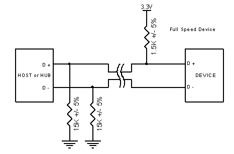
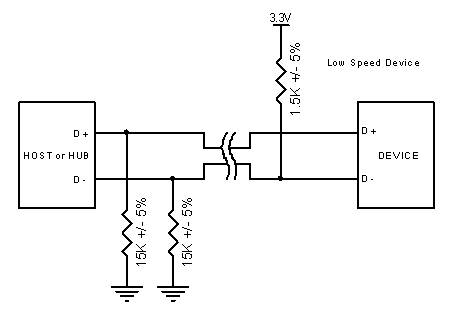
- USB uses a differential pair for data transmission. The complementary signals are D+ and D-.
- The signaling on the D+ and D− lines is within 0V to 3.3V rails, while the host supplied Vbus is 5V.
- The
USB Specification requires 15kΩ +/- 5% pull-down resistors on D+ and D-
on the host side. These pull-down resistors will condition the data
pins LOW, indicating that data transmission is not possible in that
condition.
- A USB device indicates its speed to the host by
pulling D+ or D- to 3.3 volts with a 1.5kΩ +/- 5% resistor. From the
voltage divider equation, it follows that the voltage on the data line
that is pulled high becomes 3.3V(15K)/(1.5k+15k) = 3V
- If the device pulls D+ HIGH (D+ – D- = 3V), it identifies itself as a Full Speed device to the host.
- If the device pulls D– HIGH (D+ – D- = -3V), it identifies itself as a Low Speed device to the host.
- If D+ nor D– is pulled HIGH (D+ – D- = 0V), the host does not see the device.
- If the device pulls D+ HIGH (D+ – D- = 3V), it identifies itself as a Full Speed device to the host.
Serial Peripheral Interface (SPI) - https://learn.sparkfun.com/tutorials/serial-peripheral-interface-spi
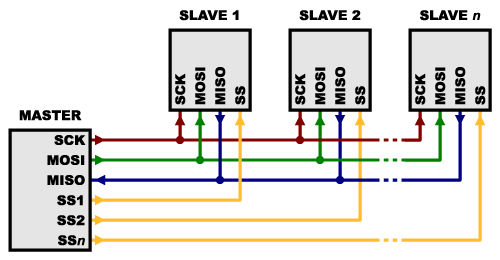
- SPI devices communicate in full duplex mode (separate send an receive lines) using master-slave architecture. There is always only one master (usually a microcontroller), but there can be multiple slaves.
- There are 3 lines (MOSI, MISO, SCK) common to all devices and one line (SS) specific for every device.
- MISO (Master In Slave Out) - Slave line for sending data to the master.
- MOSI (Master Out Slave In) - Master line for sending data to the peripherals.
- SCK (Serial Clock) - Clock pulses synchronizing data transmission generated by the master.
- SS (Slave Select) - a pin on each device that is used for waking up / selecting the slave with which the master wishes to communicate. SS is active low, meaning that a device is awaken when its SS line is pulled low. This enables multiple devices to share the same MISO, MOSI, and SCK lines.
- Only the master side generates the clock signal.
- The master must know in
advance when a slave needs to return data and how much data will be
returned. This isn’t a problem, as SPI generally talks to input devices with a very specific command structure.
- You don’t want two slaves activated at the same time, or they may both try to talk on the same MISO line, resulting in garbled data.
In-Depth Analysis
In this section, I explain the exact role of each passive component on the FabISP board. If you have a clear understanding of the prerequisites above, then most of the content here should be self evident.
20MHz resonator – provides an external clock signal to the microcontroller.
1uF capacitor – connected between VCC and GND for noise filtering<
10K resistor – pull up resistor for the reset pin
R_pullup – 1.5K pull up resistor on the D- line identifying the USB device as a Low Speed device to the host.
3.3V diodes – together with the 100Ω resistors, they form voltage clippers on the D+ and D- lines.
0Ω resistor – jumper that controls whether the board can be reprogrammed by another device.
NOTE: After you program the board, you must remove the 0Ω resistor, and you must also cut the trace leading to the VCC pin on the 6-pin programming header.
Let's now look more deeply not just at what is the function of those components, but also at how the need for those components
arises. That is, how would we reason about designing this circuit if we did not have the board as a reference.
We are interested in creating a programmer. Thus we need to first be
able to program the board, and then disable the possibility of
reprogramming it once it has
been programmed. Reprogramming the board requires that the RESET
pin be pulled LOW, which means that at other times that pin should be
pulled HIGH. In other words, we need to design the circuit in such a way
that the reset pin is HIGH by default, but when a programmer is
connected to the board it can pull the pin to LOW. Hence we need to
connect the RESET pin to both a pull-up resistor and also the RST pad.
The value of the pull-up resistor in this case is irrelevant. Any
resistor between a few KΩ and a few hundred KΩ would suffice.
Once we have the board programmed, we want to disable the possibility
of an external device reprogramming it. By
severing the connection between RST and RESET, 0V can never be applied
to the reset pin, and therefore our board cannot be reprogrammed. For
this, we could use either a jumper (0Ω resistor) that can be removed
once the board has been programmed.
When programming the board, an external device is supplying the reset
signal. But when we are using the board as a programming, it is this
board that needs to provide a reset signal to another board. Thus, our
board must be able to control the voltage at the RST pad. Hence we must
also connect the RST pad to an I/O pin.
To reduce power supply noise, we can put one or more decoupling
capacitors between VCC and GND. To suppress noise of wider frequency
ranges, we can use several
decoupling capacitors in parallel, each with different capacitance
value. The usual choices are 1uF, 0.1uF, 0.01uF.
While the ATTiny has an internal clock, we can use achieve higher
speed and accuracy by providing an external clock signal using either a
resonator or an oscillator.
The USB data lines should never go above 3.3V as per the USB
specification. However, since the ATTiny will be powered by the USB
power line (5V), the output of its I/O pins will be
~5V. Hence we need to regulate down to 3.3V the maximum voltage at the
I/O pins that would connect to D+ and D-. One option would be to use two
3.3V
regulators. But a cheaper solution is to create two voltage clippers,
each consisting of a 3.3V diode and a resistor.
To identify our board as a USB device to the host, the USB standard
requires that a 1.5KΩ pull-up resistor be connected between one of the
data lines and 3.3V. This 1.5KΩ pull-up resistor on the device side
overcomes the 15KΩ pull-down resistor on the host side, thereby pulling
the corresponding
data line HIGH. If D+ is pulled HIGH, the board would identify itself as
a Full Speed device. If D- is pulled HIGH, the board would identify
itself as a Low Speed device. On the FabISP, On the FabISP, the D- line
is the one being pulled HIGH with a 1.5K resistor connected to 5V. On
the FabOptimus, this is R_pullup. However, we notice that there is a
discrepancy between the USB specification and the FabISP, because
according to the spec, the pull-up resistor should be connected to 3.3V,
yet we are connecting it to 5V.
The proper approach for resolving this discrepancy would be to use a
3.3V regulator or clipper between the pull-up resistor and the 5V line.
However, we can get away without this extra step.
If we follow the USB spec, then the voltage on the pulled-up line should
become 3.3V*(15K)/(15K+1.5K)=3V. If we don't follow it, and connect the
R_pullup to 5V then the voltage divider
equation yields 4.55V, which may damage the host. Nevertheless, because
we have the 3.3V zener diodes connected to the data lines, the voltage
on each data line can never
exceed 3.3V. Thus we can get away with connecting the 1.5K resistor to
5V directly. Since the voltage cannot exceed 3.3V regardless of what
resistance we use, and since we don't have a 1.5K resistor in the
inventory, could we simply use a 1K resistor? Trial and error shows that
if we use a 1K resistor then we do often run into errors when reading
data from the device. Therefore, R_pullup must be 1.5K +/- 5% as the USB
specification demands.
A lingering question from the previous paragraph is why is R_pullup connected to the D- line and not the D+ line? In other words, why is the board identifying itself as a Low Speed device to the host, rather than as a Full Speed device? The V-USB package only supports Low Speed (1.5Mbaud). Full Speed is 12Mbaud. (There is also High Speed at 480Mbaud, which is 40 times faster than the nominal max speed of the processor, and clearly a non-starter). Full speed would require hardware support or much faster software emulation - it may be achievable with overclocking and very clever code.
The last question to be answered is why should the VCC pin on the 6-pin header be disconnected once the board is programmed? The expectation is that any board that we want to program with the FabISP would supply its own power, rather than drawing power from the FabISP. By disconnecting the VCC pad from the FabISP, we are ensuring that the FabISP will not attempt to power a device that is connected to it. If we don't do so, then both the FabISP and the device being programmed will be drawing current from the same USB port, and the port may not be able to supply enough current.