week 04 // electronics design
For this week's assignment, we had to create the traces for the echo hello-world board, add (at least) a button and LED (with current-limiting resistor), check the design rules, and make it. The electronics design workflow was a four-step process:
- Design the circuit in a schematic editor
- Place the components in a baord layout editor and route traces
- Mill out the PCB
- Solder all components
To accomplish the first two steps, I used EAGLE and the components from the fab library. I found three excellent tutorials on EAGLE from sparkfun: Install and Setup, Schematic, and Board Layout. The third step used the Roland SRM-20 desktop mill that we became familiar with in week 02.
04.01 // designing the circuit
Basing off of the echo hello-world board, I created my schematic in EAGLE. First in EAGLE, I had to load the fab library of parts. To do this, I copied the .lbr into the directory, under library, or open up the library tab. From here, most of the parts we needed to use were available and easy to find. The parts I used for the schematic were:
- supply1/+5V
- supply1/gnd
- fab/attiny44-ssu
- fab/resonator
- fab/res-us1206fab
- fab/cap-unpolarizedfab
- fab/avrispsmd
- fab/ftdi-smd-header
- fab/6mm_switch6mm_switch
- led/ledsmt1206
One shortcut I used in my process was that you don't have to draw lines to every part. I simple had to draw a short wire on the end of any pin and rename it using the naming tool. Any other wires with the same name are connected together internally. This greatly cleaned up my schematic design and kept those parts connected on the PCB.
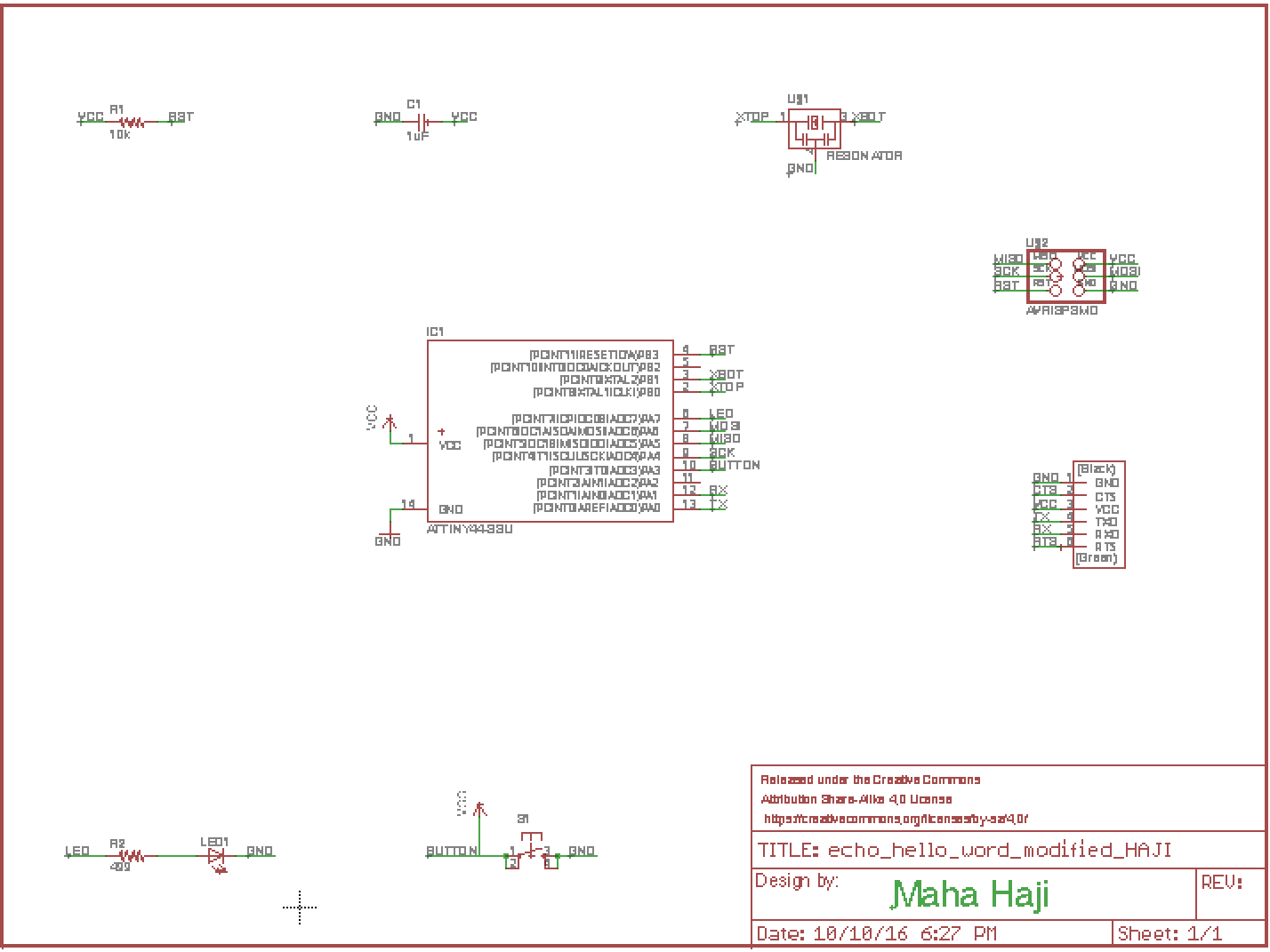
// board schematic in EAGLE //
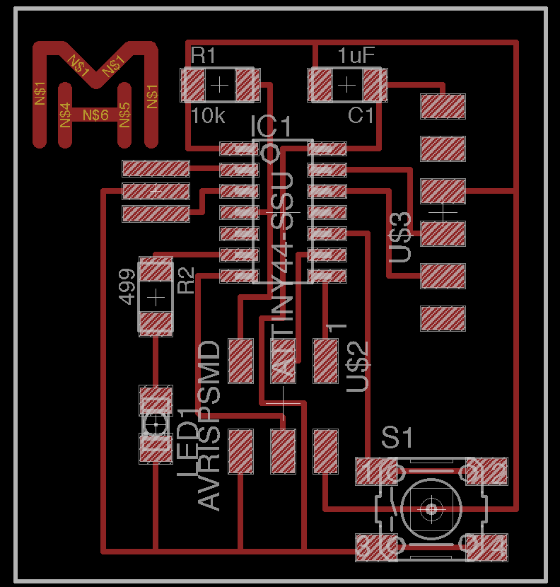
04.02 // route the traces
Once I had completed the schematic, I opened up the Board view and began routing the traces. I used the sparkfun tutorials and after a while I figured out what I was doing. First, all the components appeared on the board in a very disoriented pattern. Then, I moved them around, rotated them, and placed them compactly and redrew a new dimension around them all. After that, I made the wire traces as neatly as I could. One issue I found was that I was not able to fit all three wires that I wanted to fit under the ATTINY44. After increasing the grid resolution from 0.05 to 0.005, it allowed me to move the line sin much smaller increments and that worked well. I even added my own logo :). I exported to png file, saving it at 600dpi, in monochrome.
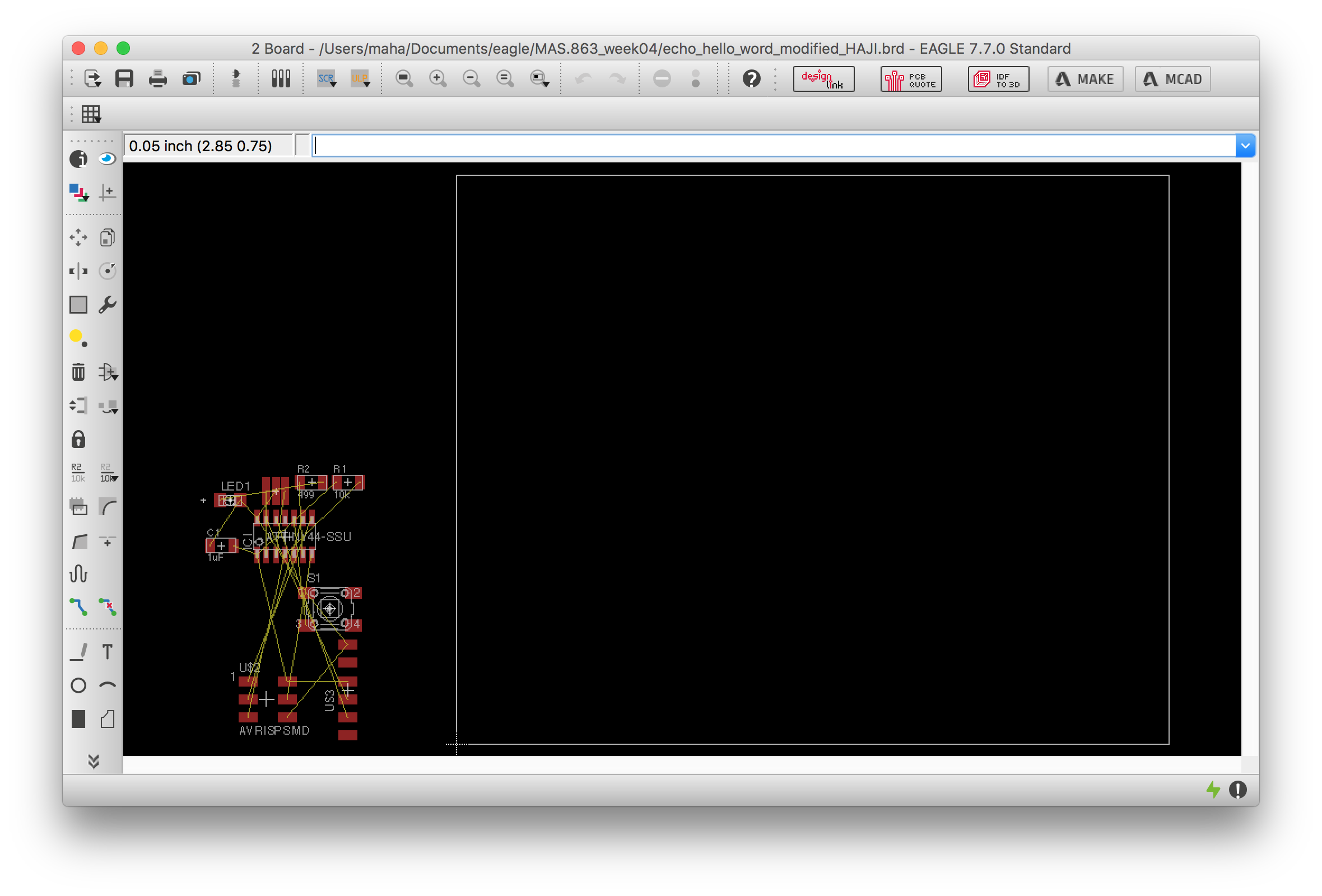
// fscreenshot of initial board view //
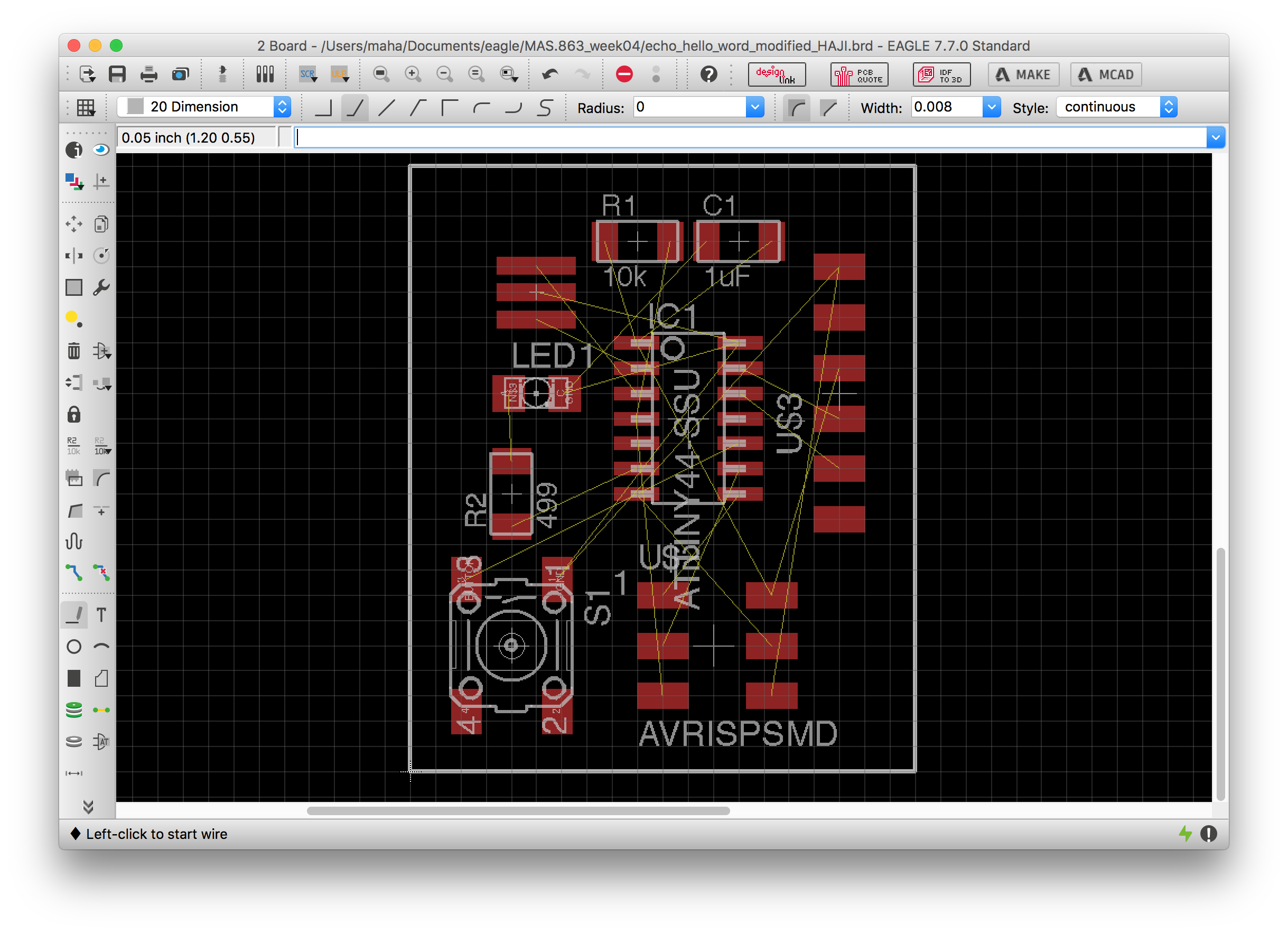
// screenshot after moving and rotating components around //
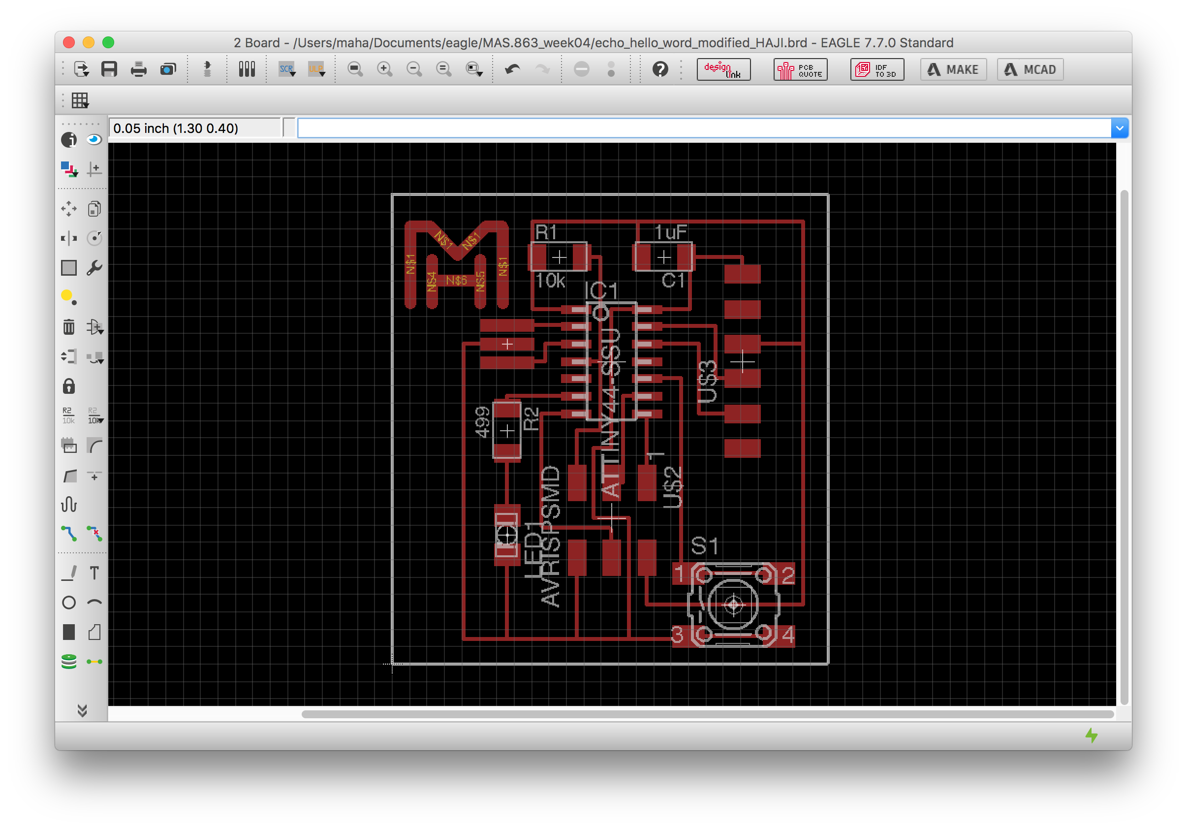
// screenshot of final traces! //
// cad of final board // |
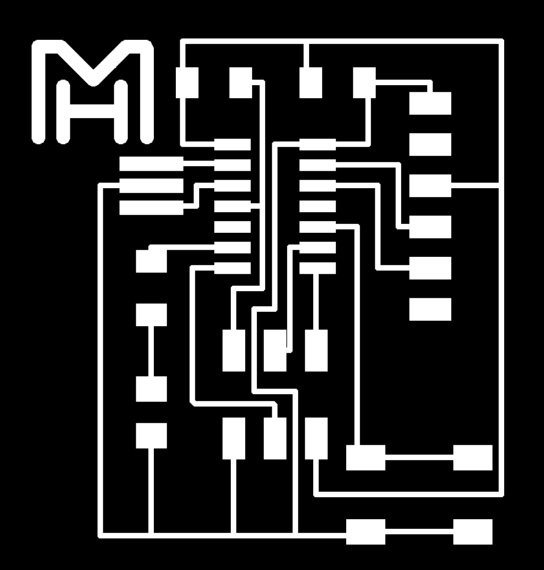
// final board traces // |

// final board outline // |
04.03 // milling the board
Following the same procedure as in week 02, I was able to sucessfully mill the traces and the outline of the PCB board.
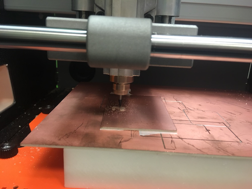
// mill hard at work // |
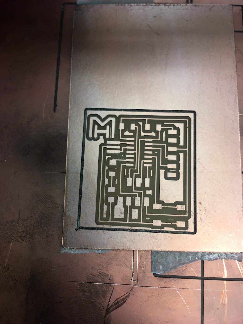
// traces milled out // |
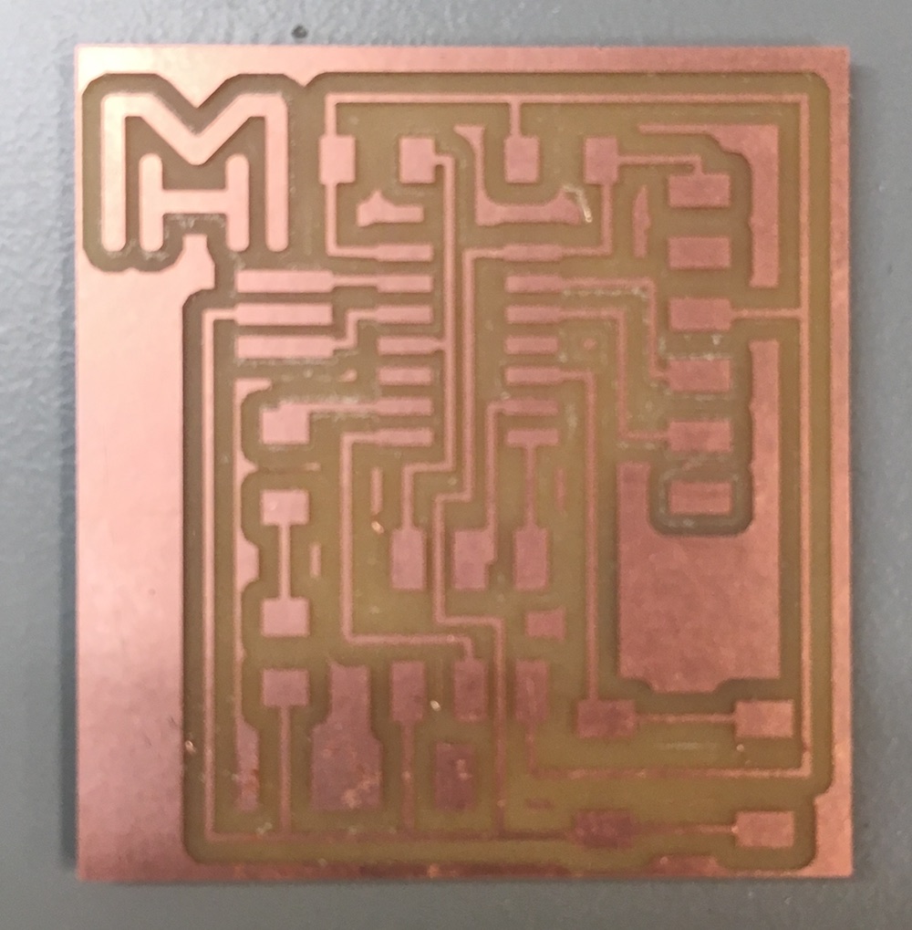
// board finished milling // |
04.04 // soldering the components
With my board in hand, it was on to the next step - soldering! As usual, this was quite a lengthy and slow process...

// one component down, so many more to go...//
After much time and patience, my board was complete!

// my first electronics board! //
Overall, the hardest part about this week's assignment was getting used to EAGLE and working with the software to design the board. It took me probably 10 hours just to get familiar with the software and use it to successfully design my board. Now that I am used to the software, I have a feeling that future board designs should be much, much, easier.