week 10: input devices
This week's assignment was to measure something. We needed to add a sensor to a microcontroller board that we designed and read it. For my final project, I need to be able to sense when physical music notes are placed on top of a surface with the lines for a musical staff. I think step response is the best place to start, so I wanted to create a step response input device this week.
I referred mainly to Matt Keeter's multitouch board for designing my own. He created a 4x4 grid in his design. For my final project, I will need more than 4x4. Ignoring below and above the bottom and top staff lines, there are 9 locations where a music note can be placed, so if I wanted to allow someone to place 4 music notes, I would need 9x4. I thought it would be too much to start with 9x4, so I figured the board I design this week won't be the board I use for my final project.
In Eagle, I created the schematic for a 4x4 step response board. When I began trying to organize the board, I got overwhelmed, even though I was referring closely to Matt's design. I decided to simplify my board since my final project dimensions would be different than 4x4 anyways, so I switched my schematic to be for a 3x3 grid. For my first attempt at organizing the board, I organized most components as Matt did in his design but then continued rerouting and moving components around after I had an intial layout. One thing I found really clever in Matt's design was the use of 0 ohm resistors as jumpers. At first, I was confused by why there were 0 ohm resistors in the schematic, but it totally makes sense that adding these resistors provides a lot more layout flexibility and allows you to avoid needing a multi-layer board.
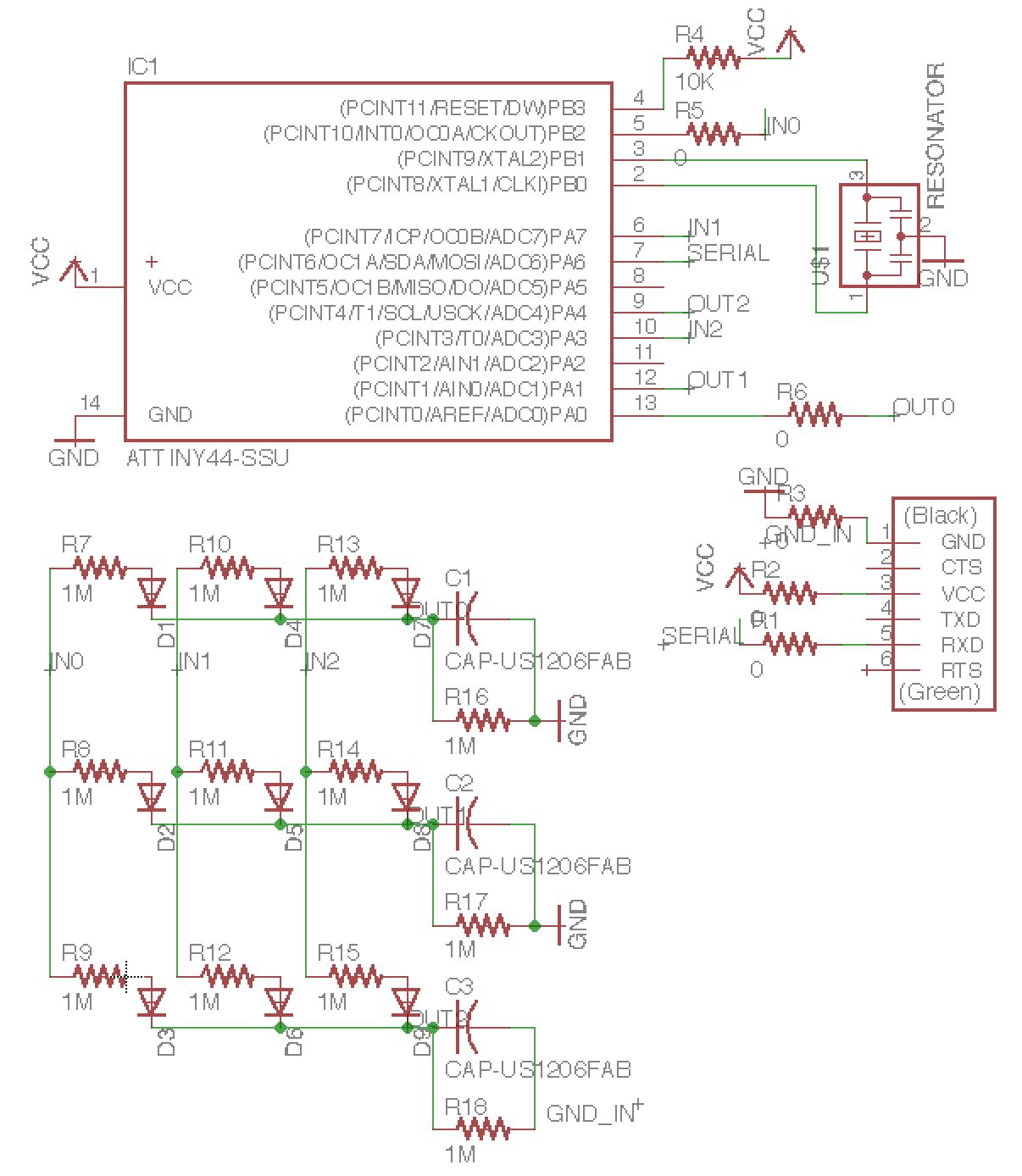
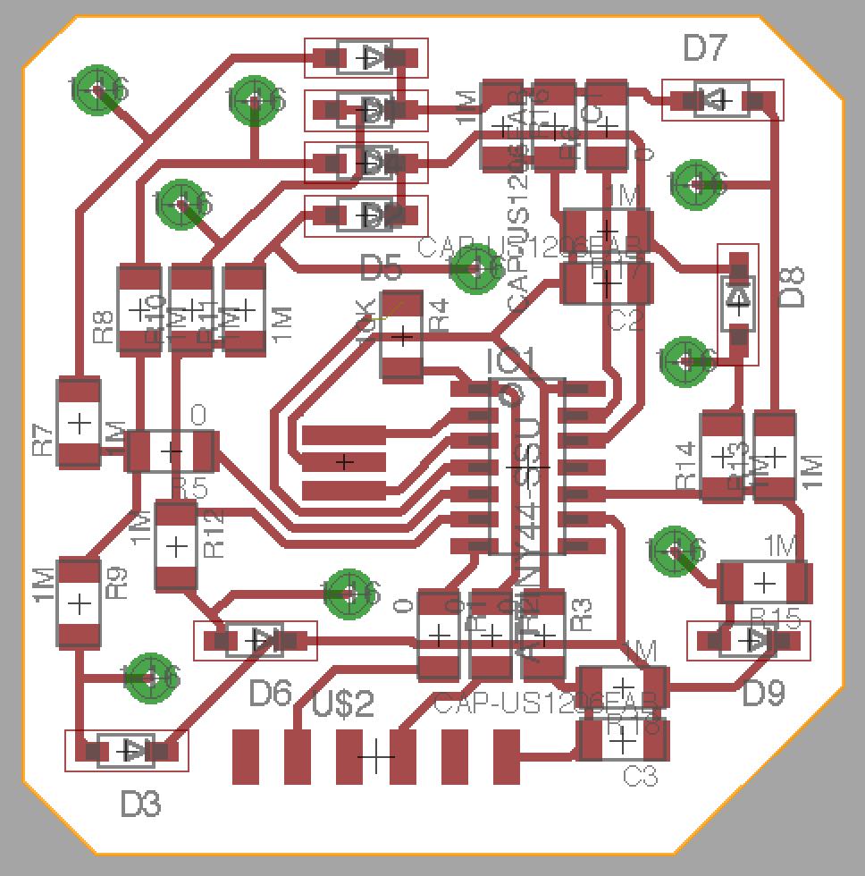
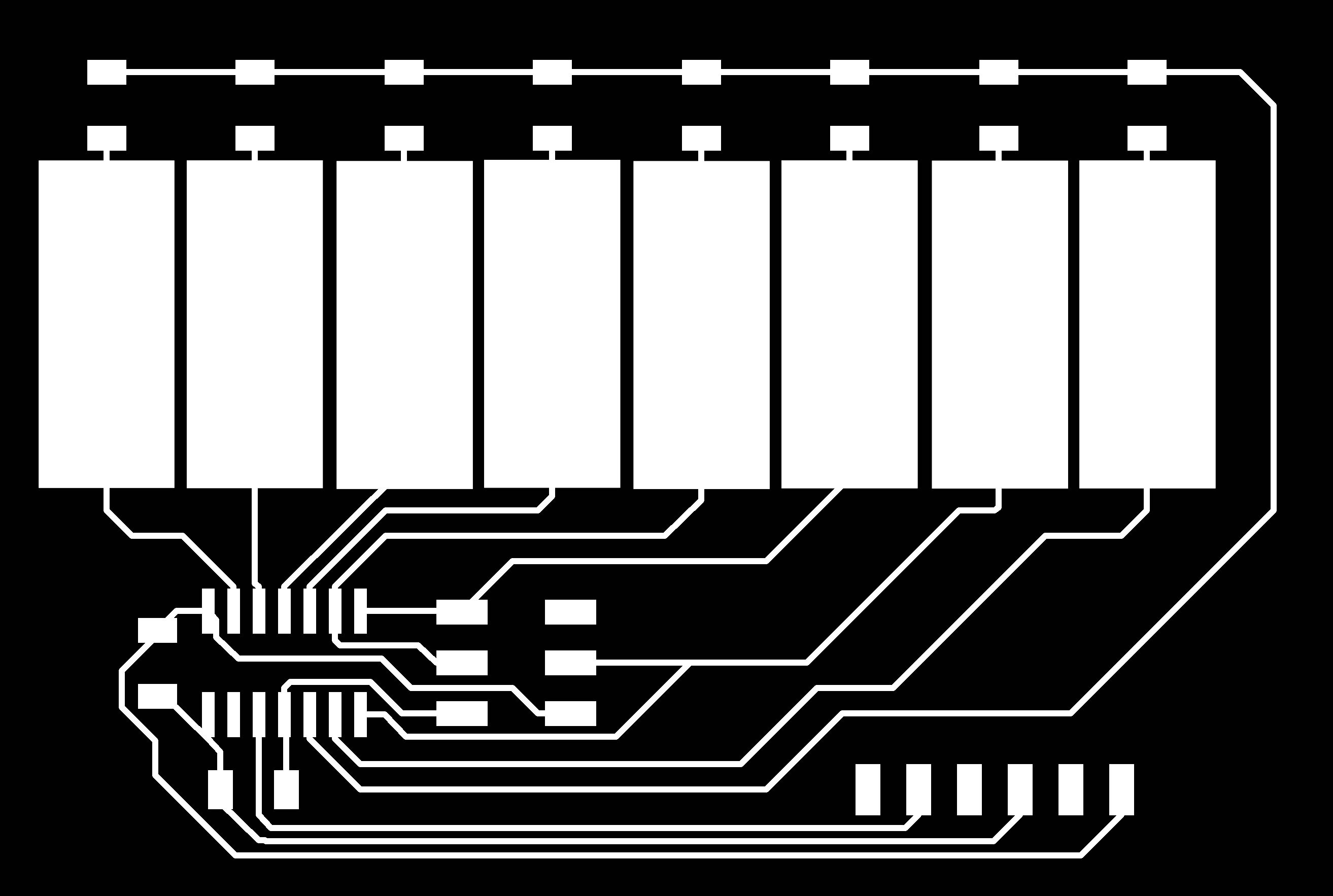
The schematic and board for a smaller version of the multitouch board.
I hadn't yet created vias in any of my boards, so I learned how to create those in Eagle. However, the vias presented me with a problem I wasn't sure how to deal with. Basically, I need to export the png images from Eagle to use from Mods to actually mill the board, but every via has a label on top of it that partially covers the via itself. So when I exported a png of the via layer, the via holes weren't isolated, which is a problem for actually needing to mill the board.
I can't hide the labels, and they show up on top of the vias when I export.
Since I was confused about milling the board with vias, I posted an issue on GitLab asking about it. Ben responded and recommended that I use the Othermill rather than the Roland to mill the board. When I went to EDS to mill the board, Ben happened to be there and took the time to show me how to use the Othermill. I was really impressed with it. With the Othermill, you never have to manually lower the end mill to touch the top of the board, and the machine actually moves the bed slightly in the z axis throughout the milling process.
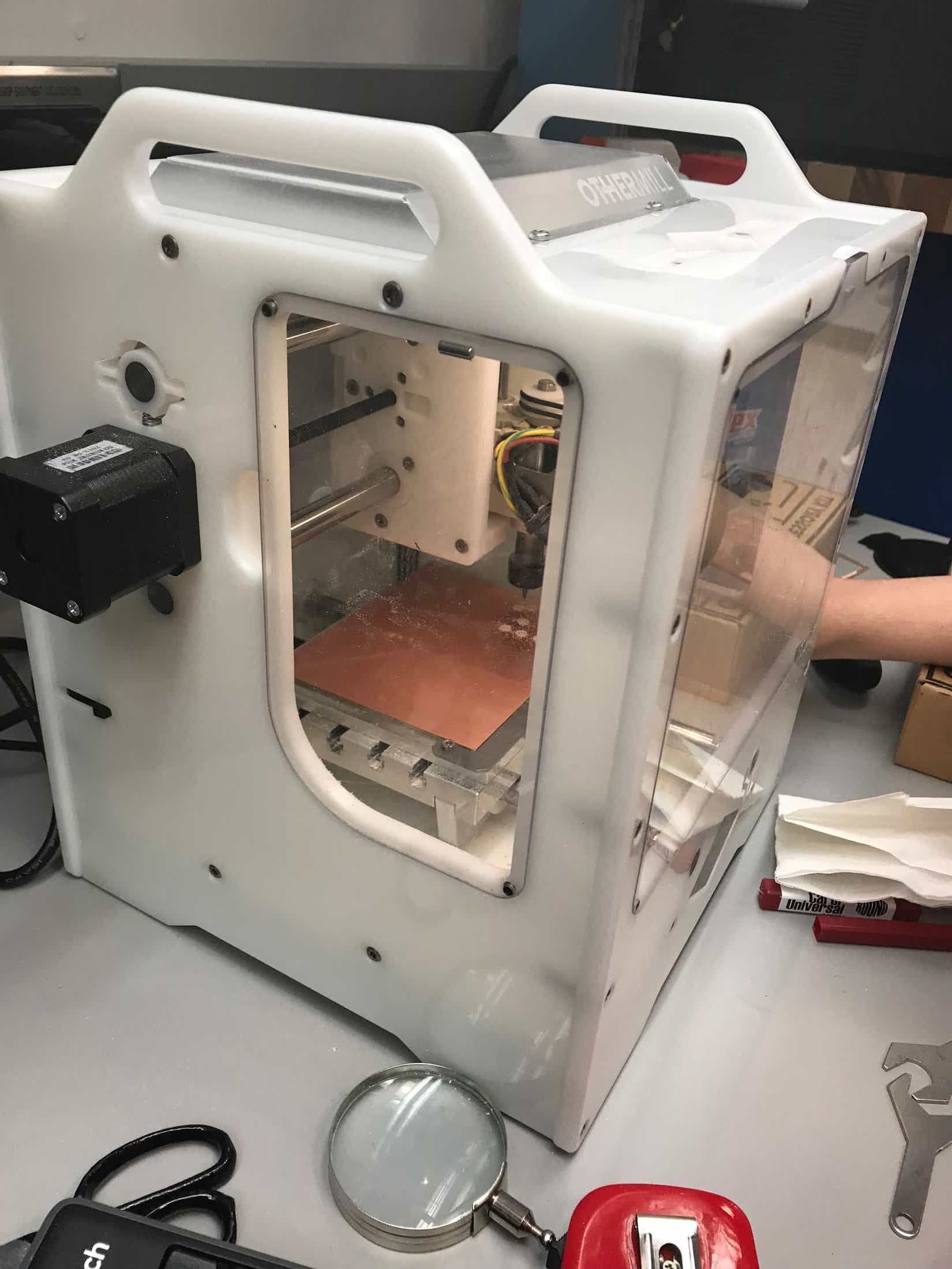
I was impressed with the Othermill.
I was milling onto two-sided copper, so Ben recommended that I isolate the vias on the bottom side. I flipped the sheet over and milled the isolation circles. They were off-center compared to where the vias were located. I'm not sure what caused this, since I aligned the copper sheet against the front right when I flipped it over. Ben said he'd never had it be this misaligned before. For the purposes of this board, it should be fine.
The board came out really nice, but the isolation holes on the backside were misaligned relative to the vias.
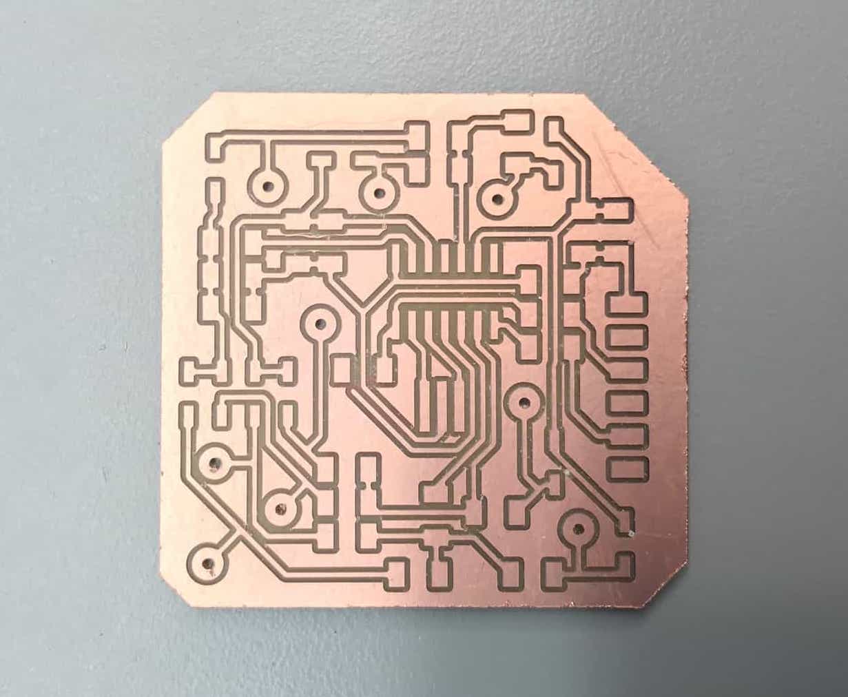
While I was having trouble with Eagle and figuring out how to do vias, I designed a simpler step response board to test before I get to the multitouch one. I referred to Akash Badshah's page for a design in which pressure-sensing pads are present on the milled board itself. I created the schematic, and then laid out the board in Eagle. I didn't know how to add custom-shape pads in Eagle. I Googled and found a couple posts about how to do it, but I couldn't get the pads and routing to both be how I wanted them. So I did the routing in Eagle, leaving room for the eight pads. I exported the png of the traces and used Preview to add rectangles into the image.
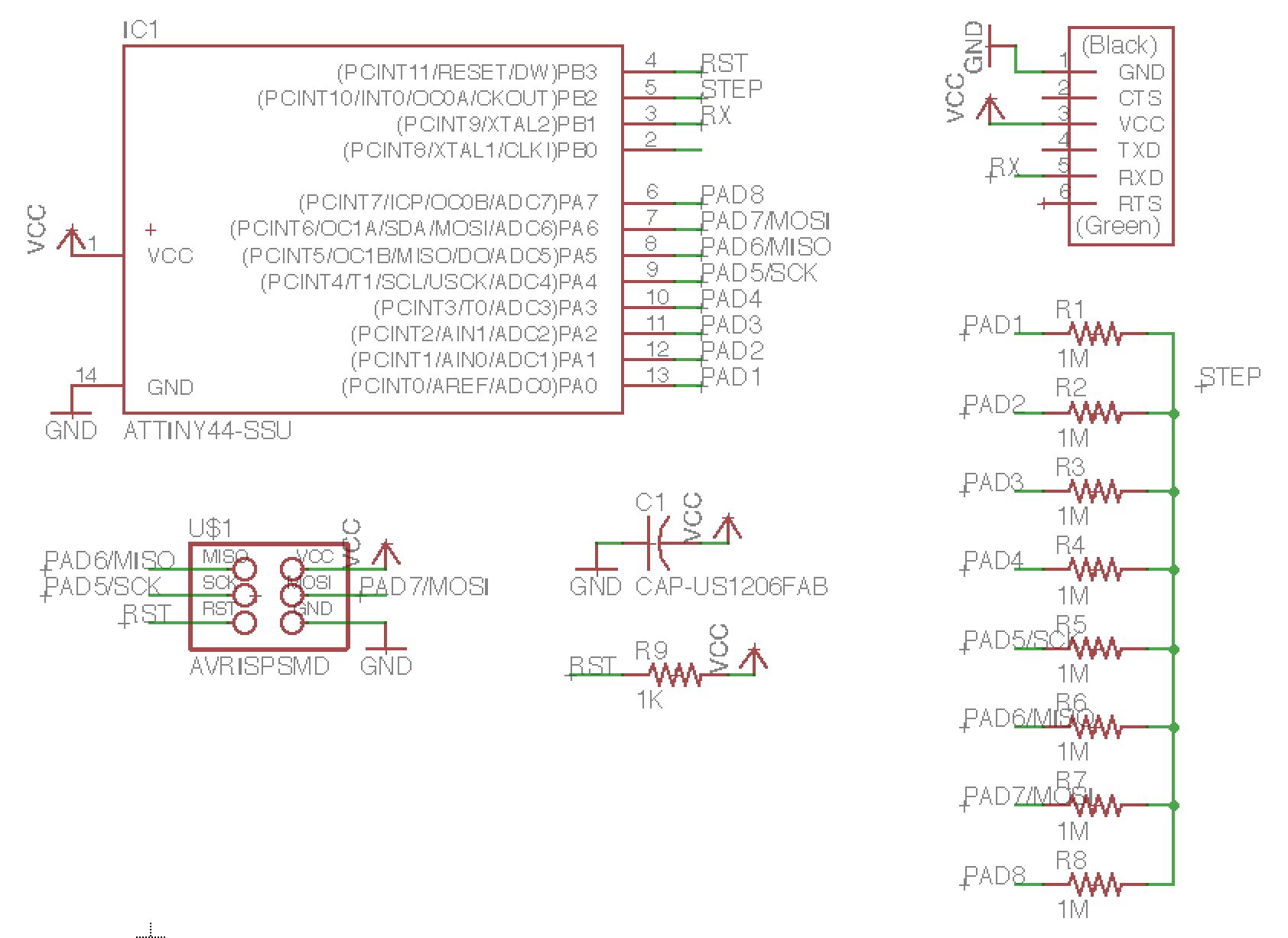
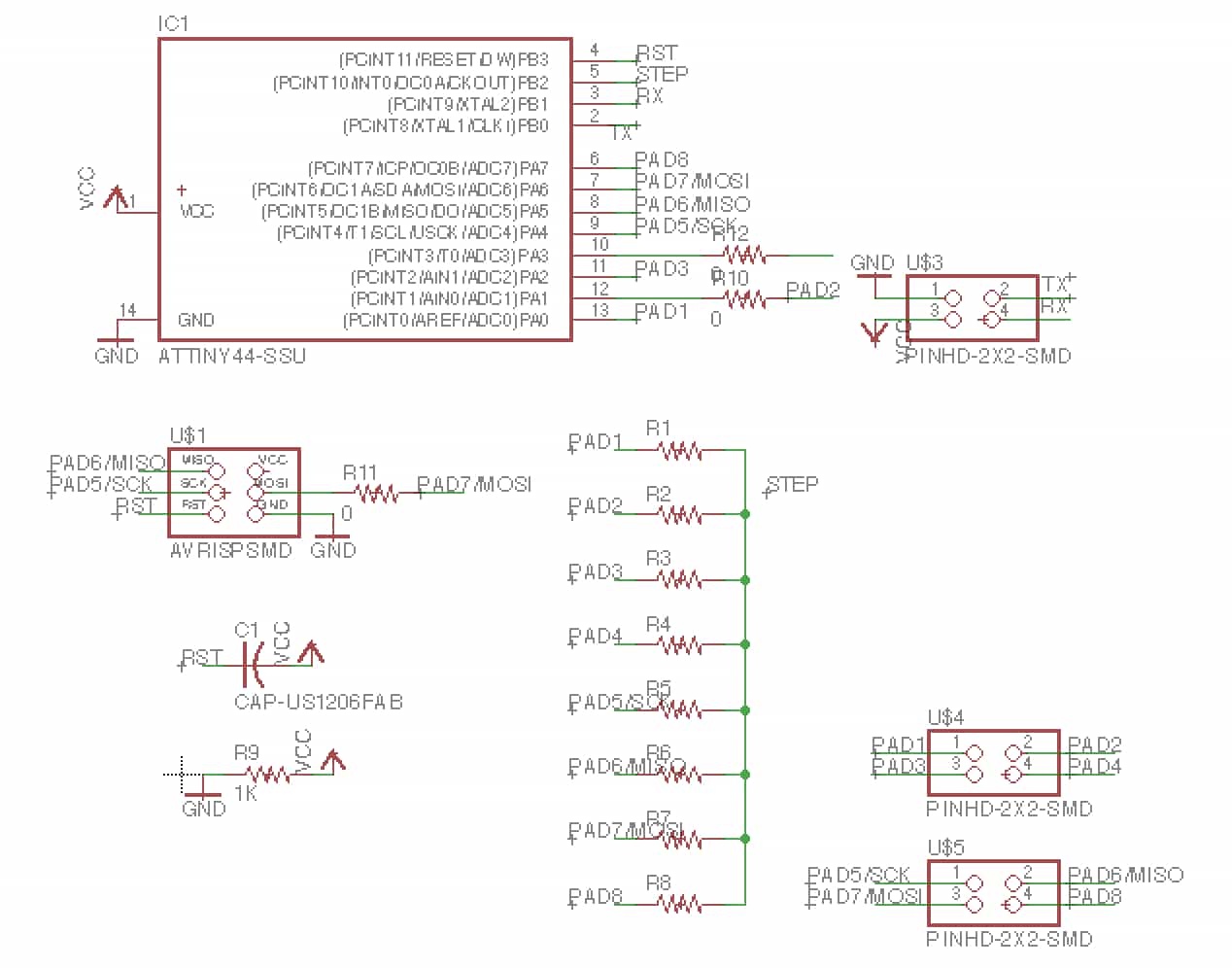
The Eagle schematic.

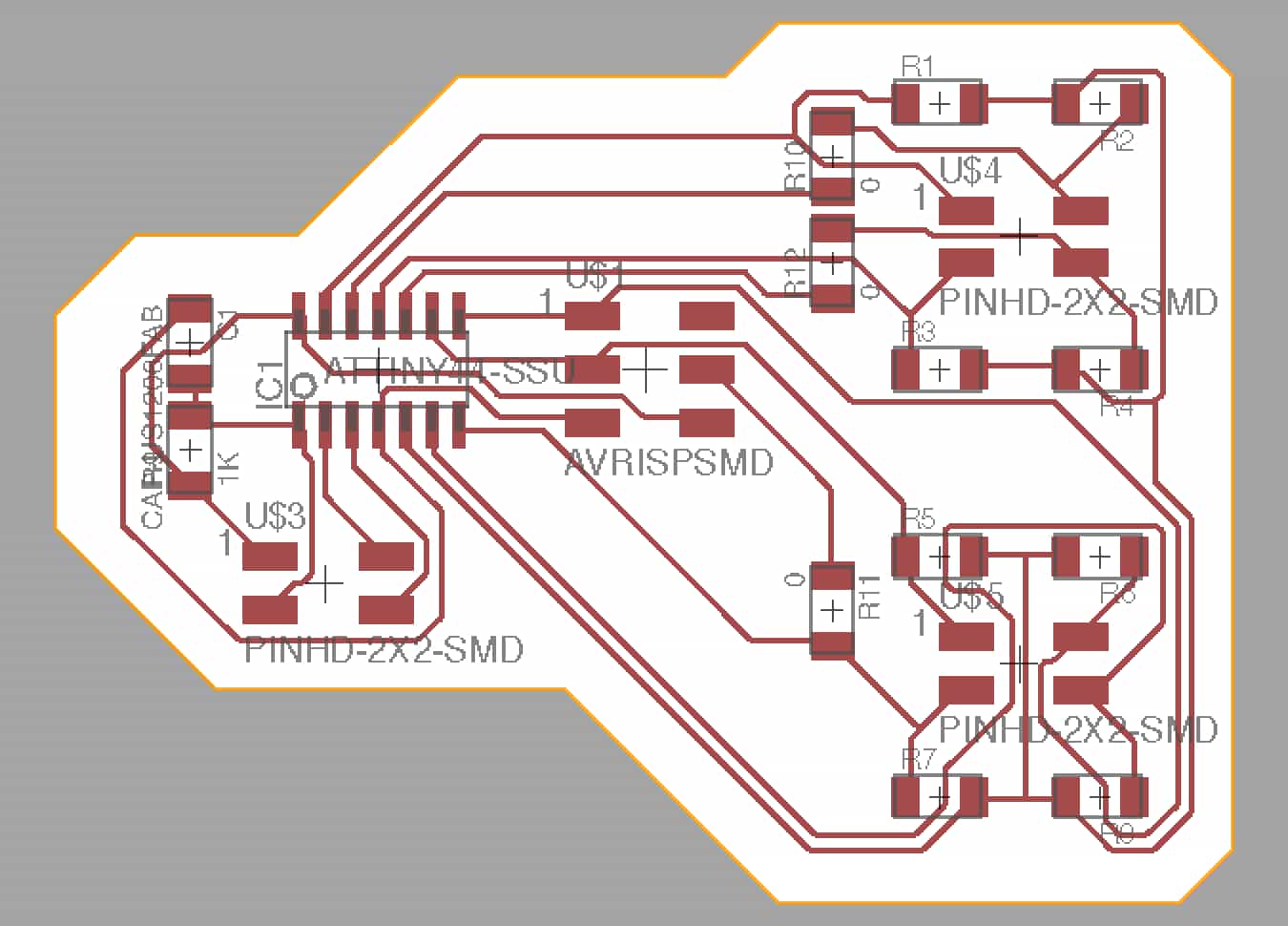
The png files for the traces and outline.
It took me multiple tries to mill this board. On one, I accidentally had the 1/32" end mill inserted instead of the 1/64". On another, the copper plate was slightly uneven so not all the traces got cut out. On my third attempt, the end mill got really gunked up with material (mostly the double-sided tape that we use to secure the copper sheet to the sacrificial layer). As a result, the board didn't come out nicely, but I thought it might be good enough to work (and if not, I could do some extra soldering to fix the problem areas).
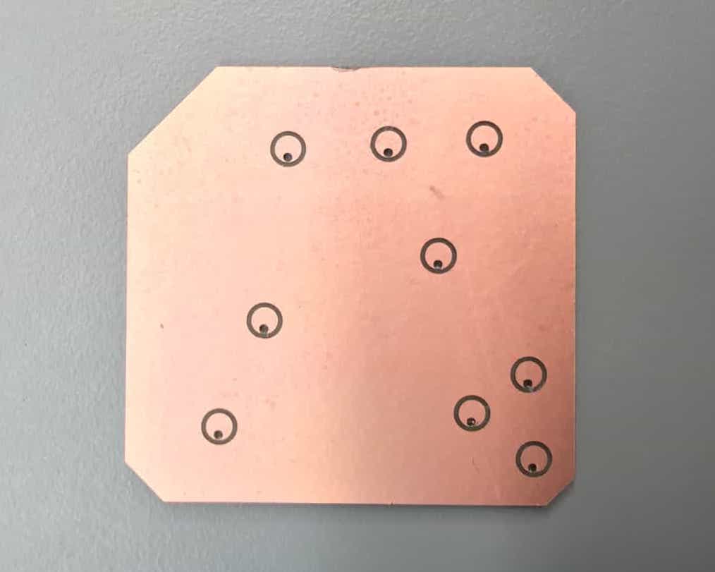
I soldered all the components to the board without any problems. I was still a bit worried about some of the traces because the board wasn't milled nicely, so before I tried to program it I used the multimeter to test it. To my surprise, the connections I was worried about actually read correctly on the multimeter, so I was hopeful that it would work. But I ran out of time to program it and see if the step response input actually works. I have the code ready to go, so I'll do this before next week.
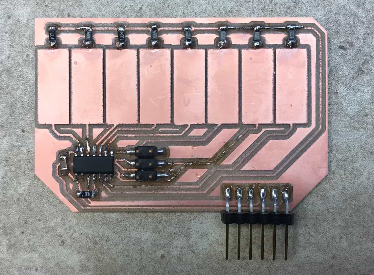
The soldered board.
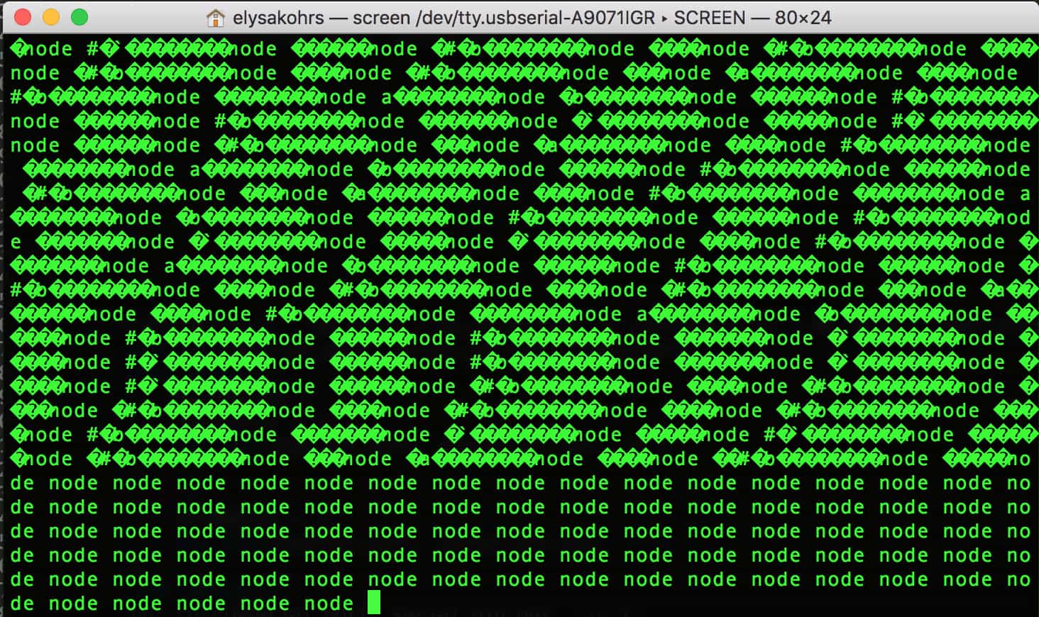
When I tried to program my board, I couldn't program it. Blah I hate the rc=-1 error.
I attempted to use the step response input device in my final project, but ultimately didn't. When I modified my final project idea to be a physical keyboard, I wanted to be able to sense when a key was pressed. I designed a version of a capacitive touch board that would connect via pin headers to eight conductive pads. The board was designed to be a node in my serial bus network. I was able to program the board, so I made more progress than before. It responded to its id in the serial network. If I programmed it to send back a predetermined character or string, it worked. But when I tried to relay the step response value or a variable value, I either saw weird symbols or nothing. Here are the designs for the step response board that I hoped to use in my final project.
Designs for the capacitive touch board I wanted to use in my final project.
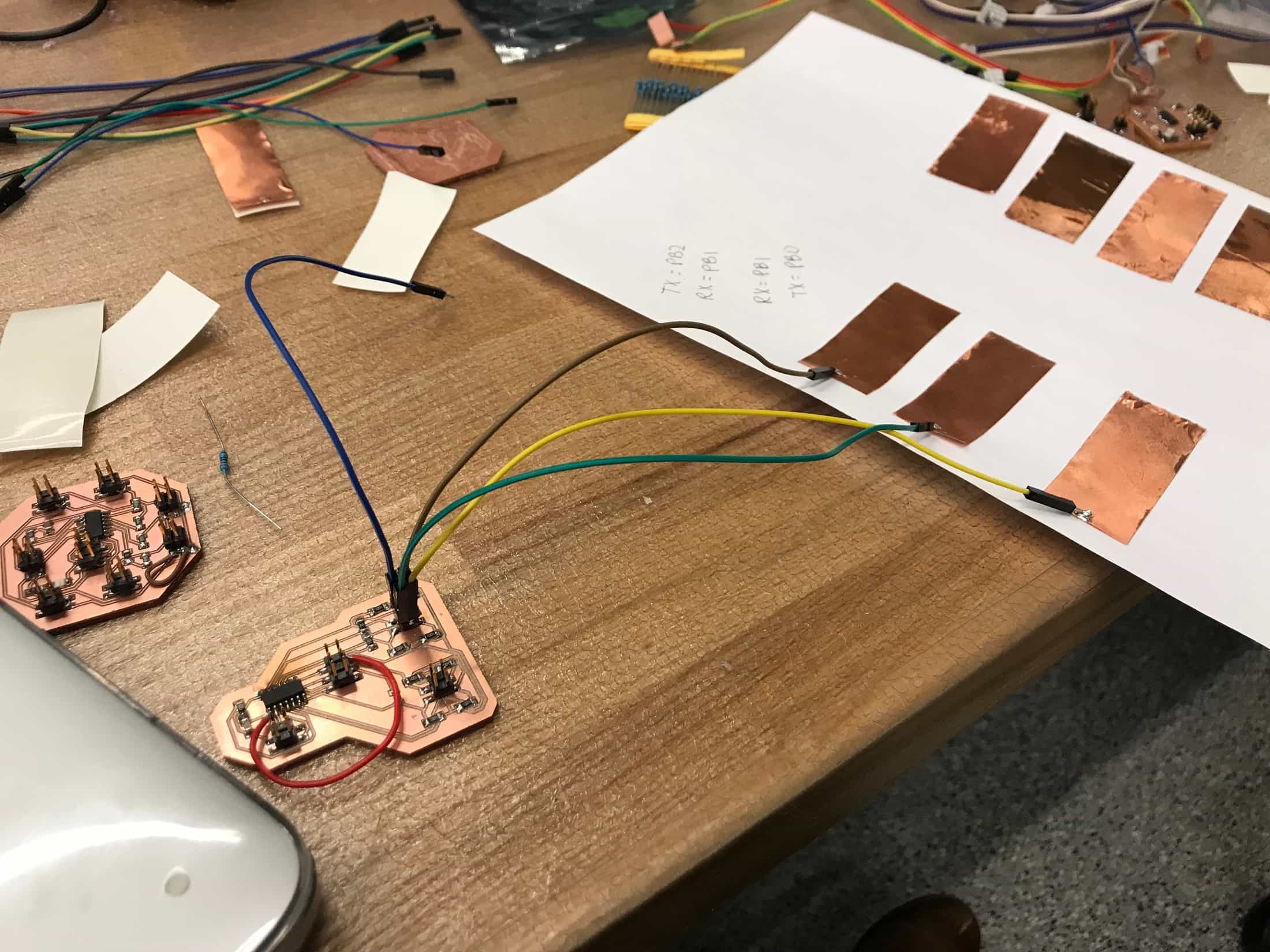
Testing the board.