assignment
Now that we have a fair amount of experience in electronics design and production, we were tasked with creating a board that senses some valuable form of input. I decided to have this week overlap significantly with my final project and created a multitouch board that one day could function as the frets on my electronic guitar.
electronics design | |
|
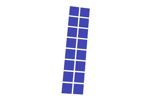
Thankfully, I was not the first person to attempt to create a multitouch surface. Matt Keeter had also designed a board to do the same thing, and I followed a lot in his footsteps. Hugely different, though, was the layout of the boards. Matt's was a 4x4 grid of touchpads. Figuring it would be hard to build a guitar out of 4x4 touch pads, I decided to make the board long and skinny, where a single microcontroller processes two strings for eight frets. Matt's design used four pins on the ATTiny44 to provide impulses to the RC grid, and then four different pins to sense the step response. |
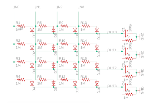
The 4x4 grid of touchpads, powered by four input pins and four output pins. |
|
I effectively learned that if you want a board with a*b touchpads (in this case, 4x4=16 touch pads), you need a input pins and b output pins on the ATTiny in order to provide the step and read the step response. So, I could have used 2 inputs and 8 outputs, but this would require 10 pins. Effectively, you want to minimize a+b. Also new is that Matt's board didn't have a programming header... I'm guessing he installed a bootloader on the board by connected probes to all of the necessary pins and then programmed the board through the FTDI header. I didn't want to deal with this, so I added a programming header and had to reuse some of the programming pins for this grid and used switches for this. |
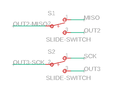
Switches to reuse programming pins. |
|
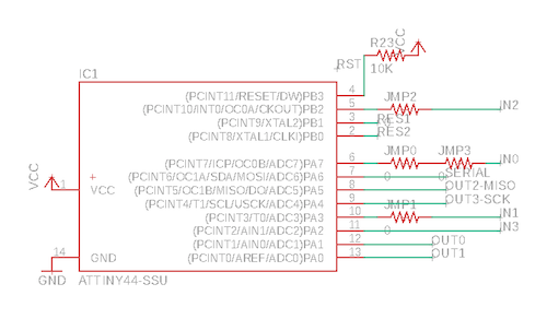
The processor then iterates through providing steps at certain pins and reading at certain pins. It does this fast enough to appear as if it is sensing all touchpads simultaneously. Finally, I ensured that all pins that read from the touchpad network were on PA pins that can be used as ADC pins. |
|
|
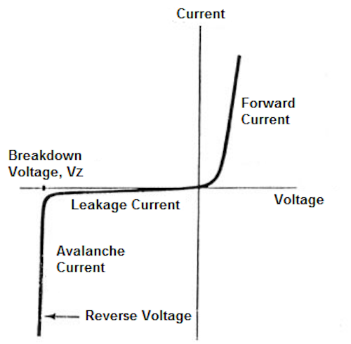
After initially designing the boards with 3.3V zener diodes to separate touchpads that shared outputs, I realized that Zener diodes allow current to leak backwards (see IV curve on the right). What I really wanted was a shottky diode, which only allows current to flow in one direction, properly isolating the touchapds. |
Zener diode IV characteristic. 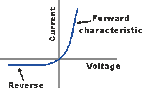
Shottky diode IV characteristic. |
|
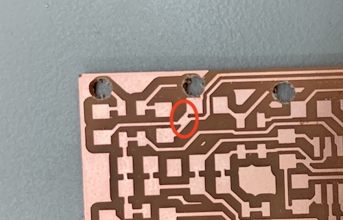
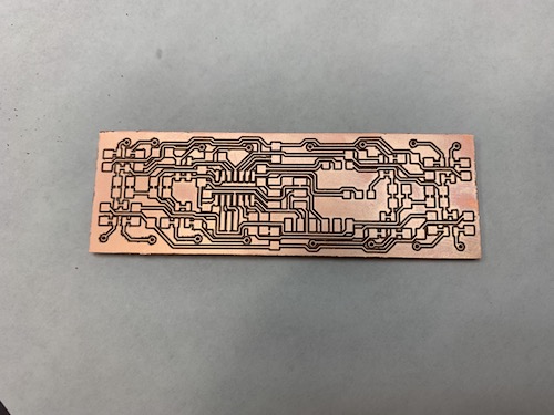
My first attempt at routing was absolutely atrocious... The hard part is that four touchpads all share a step response output and should ideally be close together, but each of those four has a different step input. So, there were at least four traces that have to span between the four sets of output step responses. I foolisly tried to simply make the network of touchpads symmetric and pretty, but this lost me a lot of space... |
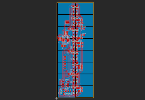
My first terrible attempt at routing. |
|
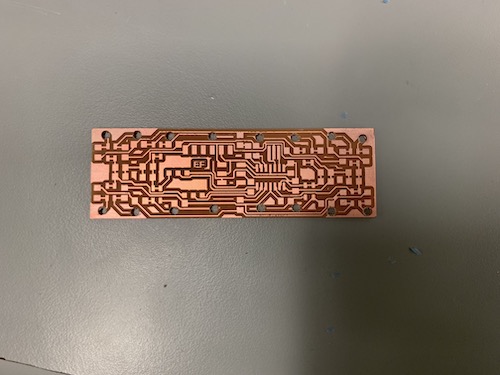
After being ashamed to have designed such a space inefficient board, I threw it all away and started from scratch, putting the ATTiny in a central location this time. This ended up looking much better... Here is the second routing job I did. The yellow outline shows the size of the first iteration of the board I created... I used a handful of jumpers and also moved pins around in the schematic to make things easier to route. |
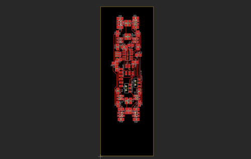
My second, much better attempt at routing. 
|
board production | |
|
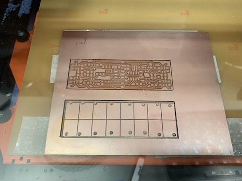
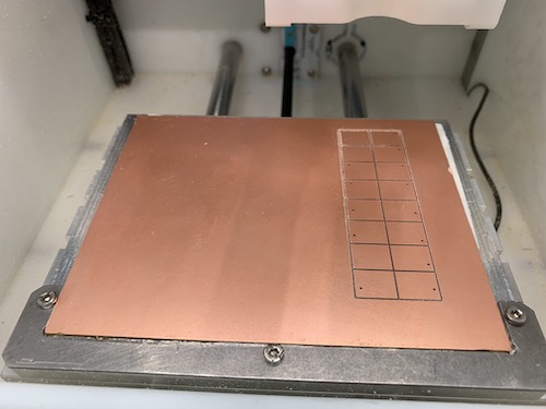
Now it was time to cut again. I first tried to cut out this board on the Roland SRM-20. Since this board was is sided, I ran into a few problems on the SRM-20 which takes pngs of the board traces and outlines... After my first attempt, I realized I had cut the vias on the back of the board, meaning they would be mirrored on the top of the board from what they should be. I couldn't flip the traces on the top of the board either, since components can't always be mirrored. |
|
|
Then, I also drilled out the entirety of the via instead of leaving behind the pad. This ended up cutting a few nearby traces and would have been impossible to solder. |
|
|
Lastly, when exporting boards from Eagle as a PNG, Eagle makes the resolution 2x what it is supposed to be. When loading the board images in Mods, I then had to double the dpi from what I exported, loosing a bit of the granularity of the traces. Since no traces broke my design rules, I think this DPI problem resulted in some traces being merged. |
|
|
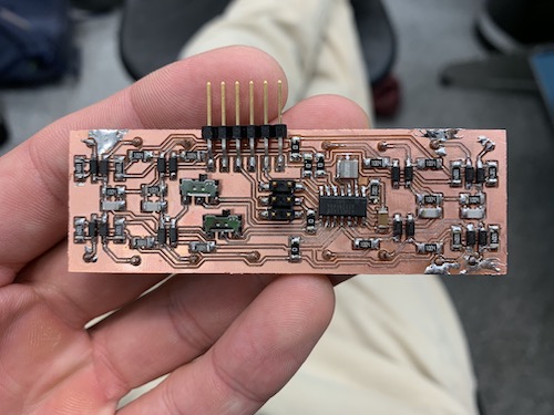
So, I cut it again on the OtherMill using Bantam Tools as the CAM software, which automatically knows which way to mirror vias and traces and whatnot. I had no problems here! |
|
|
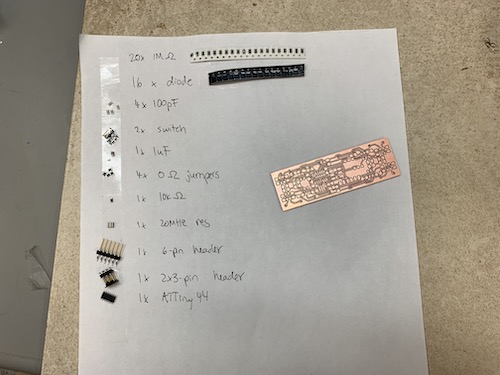
I had an intimidatingly high number of components to solder... |
|
|
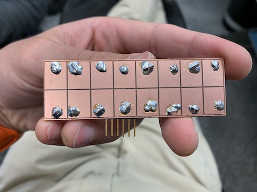
Soldering vias were tedious - I took a wire bent at 90 degrees and shoved one end into the via. Then tried to chase down one end with hot solder to fasten it to the board. With trial/error/waiting for mills/debugging, cutting and stuffing the board took me about six hours... I will surely send these to a board house if I have to make 6. |
|
software | |
|
I made a few modest modifications to the firmware on the board, simply rewiring which pins were inputs/outputs, etc. However, I could not get his visualization software to run as it was written in some strange framework. So, I decided to make a more portable web app to visualize the board. Over serial, I receive a list of ADC readings from each touchpad, delimited by hex characters that spell out "hello." |
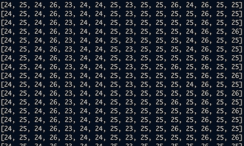
Serial readings parsed from the board. |
|
Since websites can't talk to hardware sockets on your machine, I created a simple websocket server that forwards information from the serial port over the websocket. The webpage then receives live readings from hardware through the websocket. I created a nice interface to show when each pad is touched. |
|
|
Here it is in action! You can find all the firmware and software here and the board design here. |