electronics design :
 h  o  m  e   >   >   >


what does any
of this mean ?
a newly drawn (only slightly designed) trace :

This week we were asked to "design" electronics, though I would say we aren't really designing just yet - not me anyways. The goal is to simply alter and reproduce neil's hello-world board.

Before jumping into KiCad or Eagle to draw my circuit board, I really wanted to understand, at a very basic level, what neil's hello-world board was doing.

I started by looking at a datasheet of the ATtiny24A/44A/84A.

huuuuhh?...

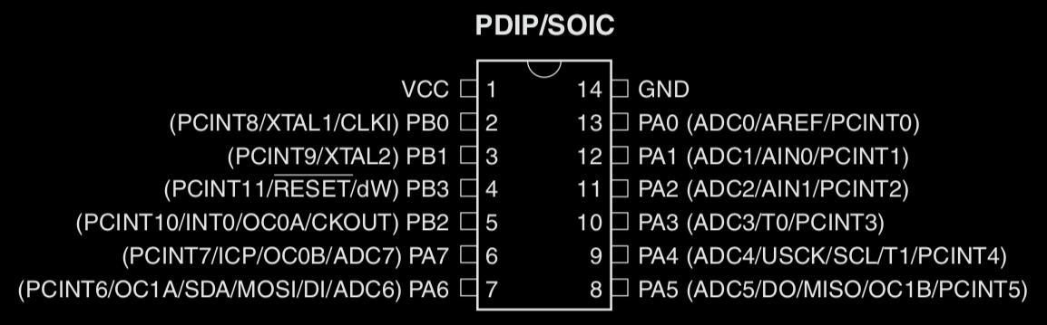
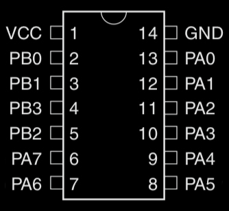
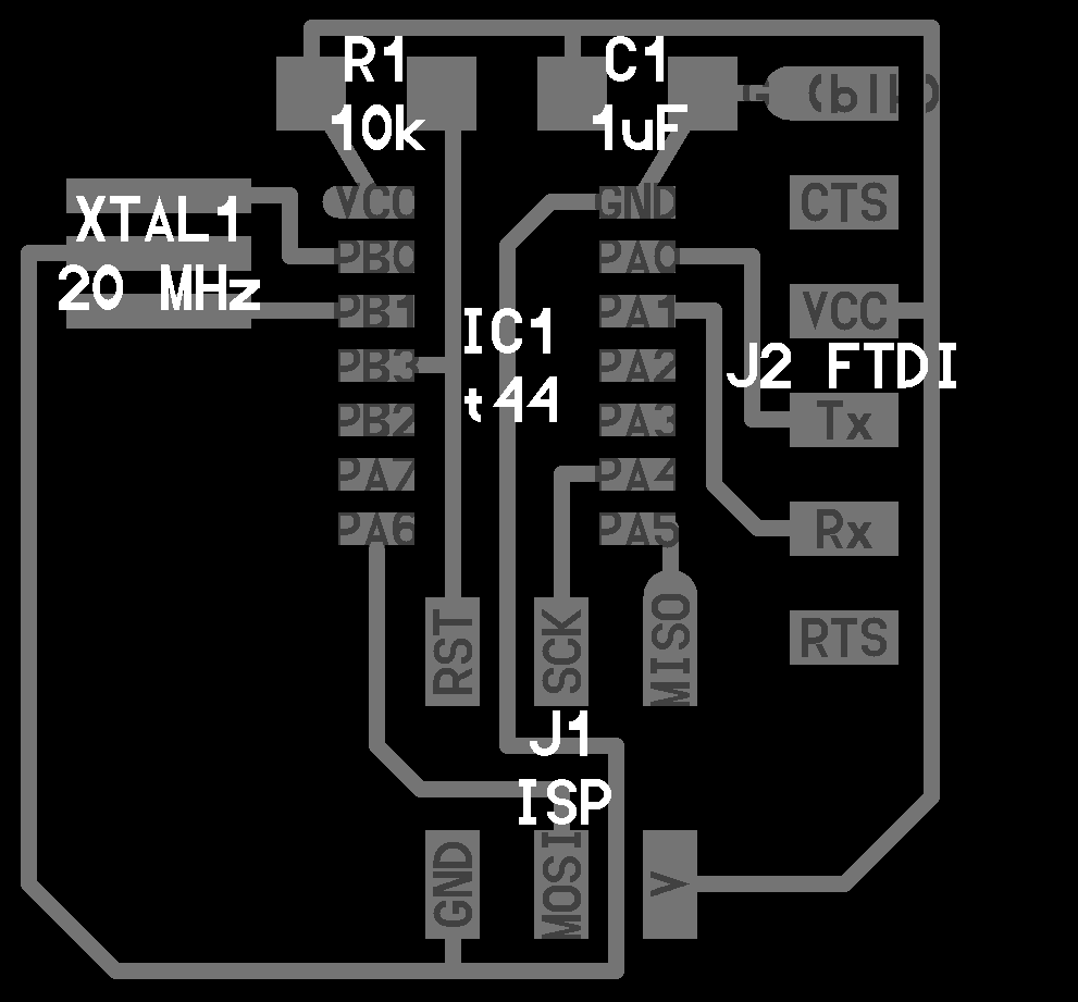
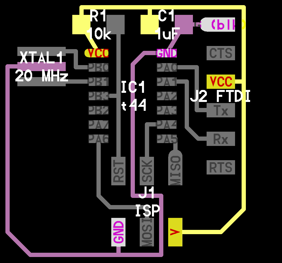
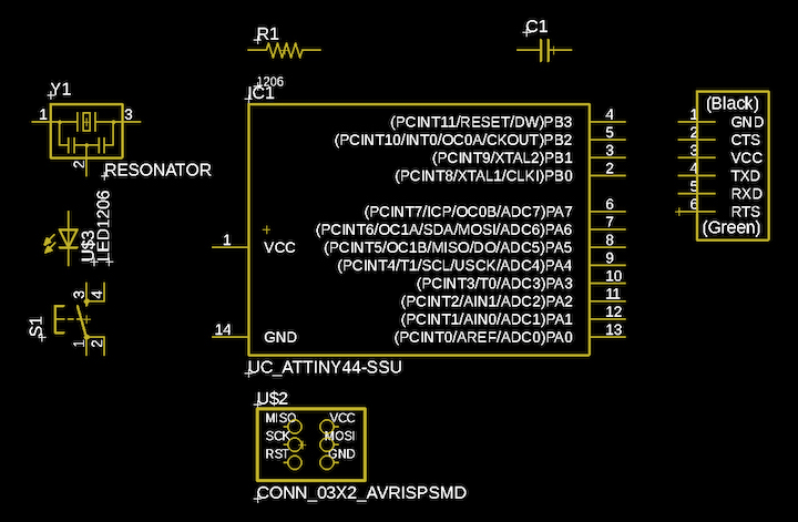
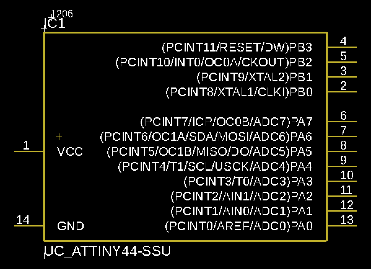
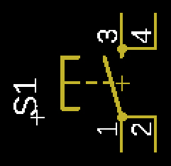
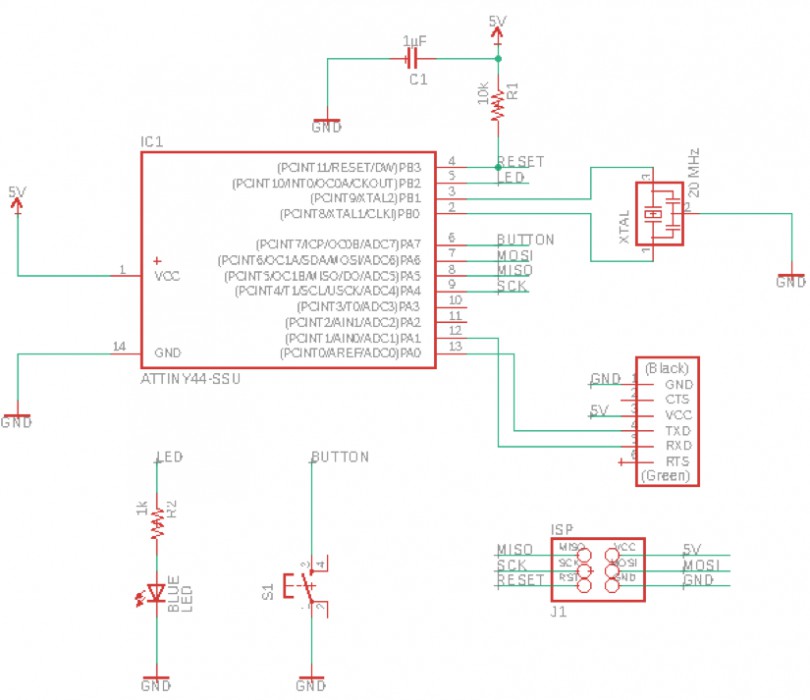
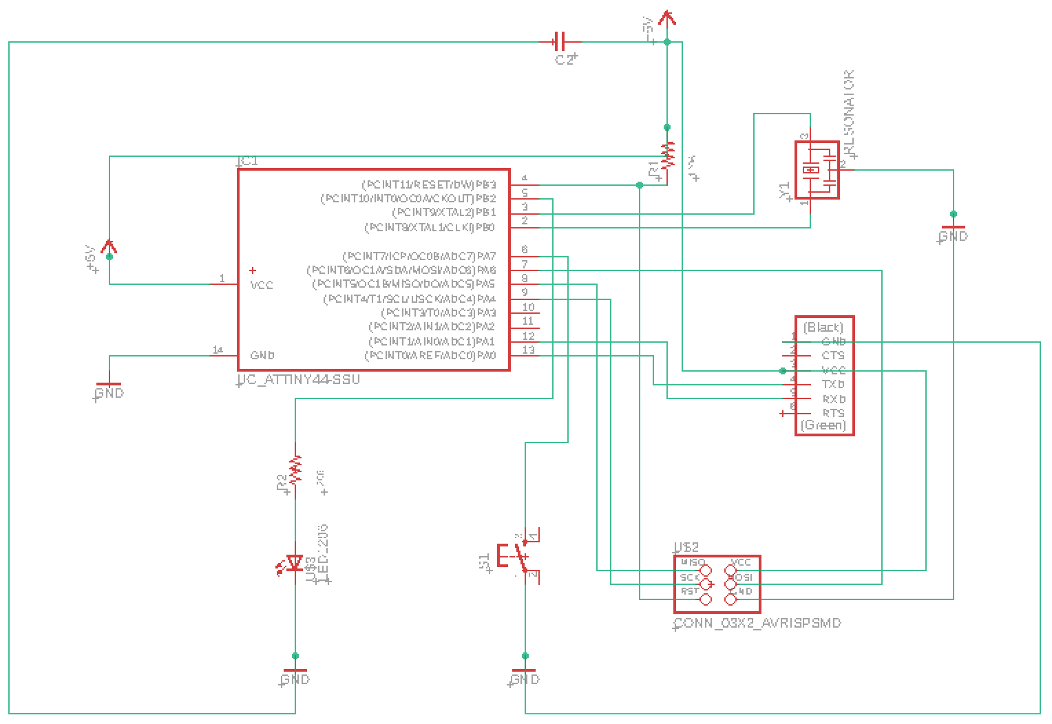
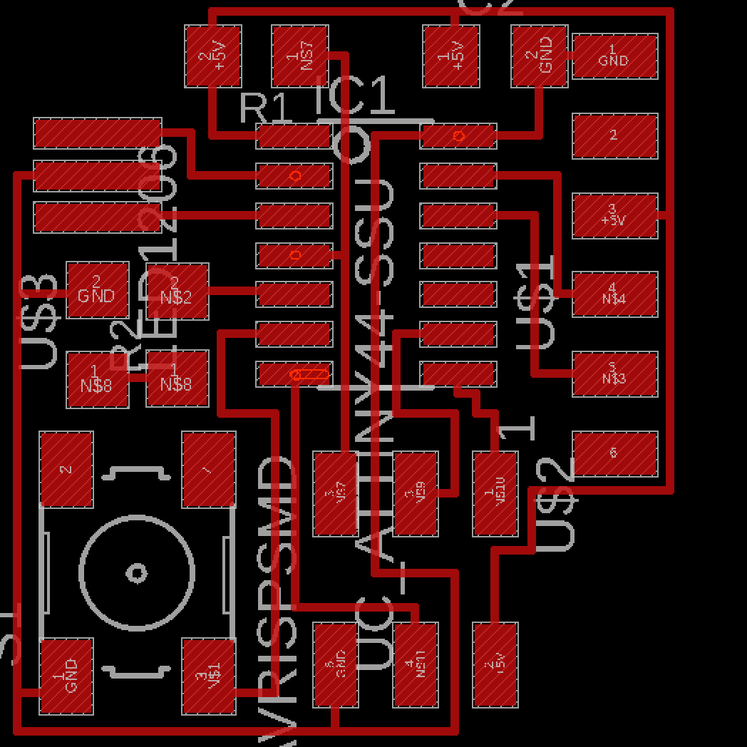
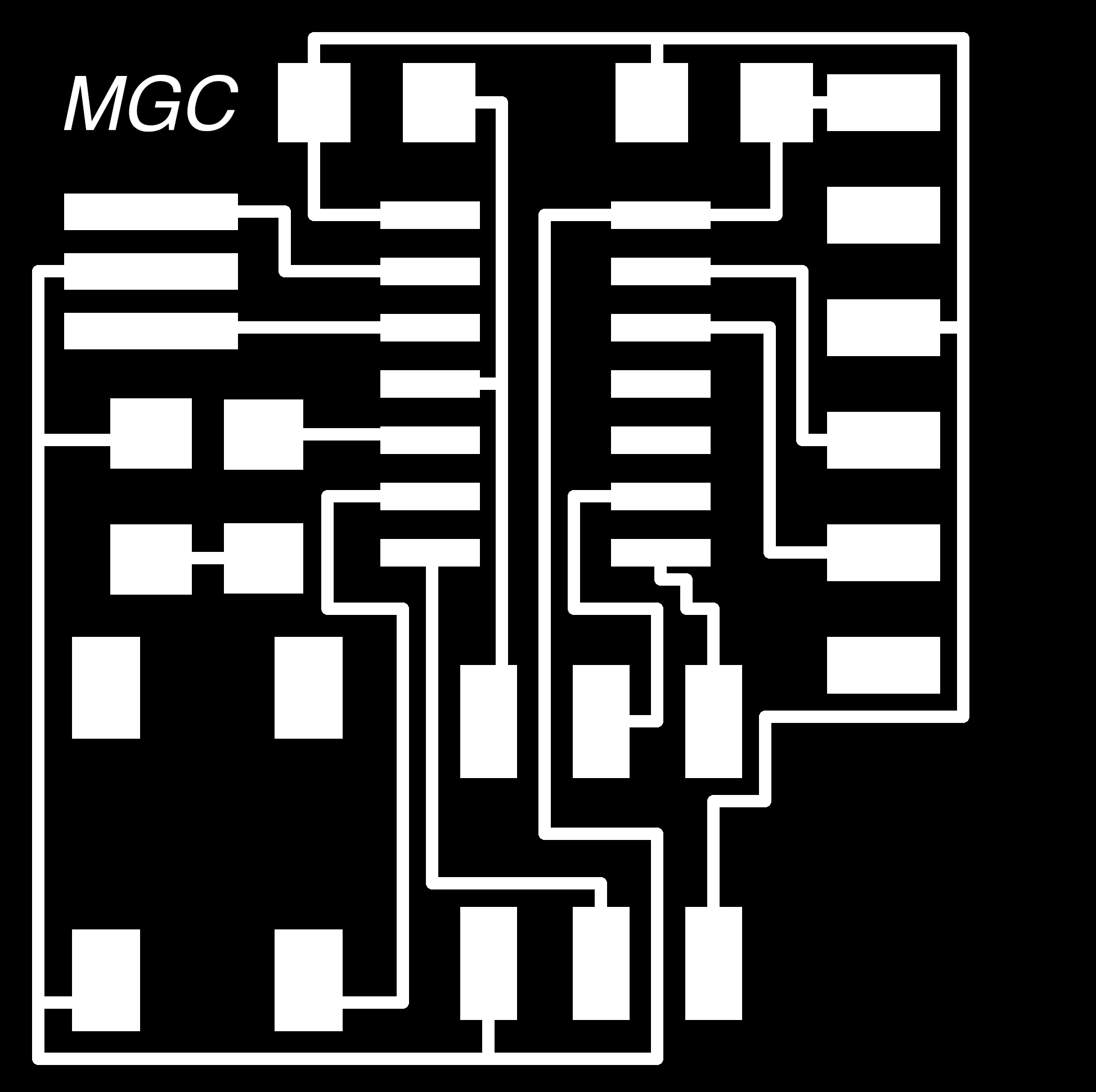
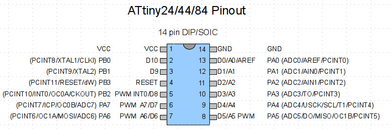
14 pins to god knows what :

The ATtiny24A has 14 pins, or connections.

I'm going to reaaally dumb down the data sheet pin descriptions for my sake :

VCC : supply voltage : in other words, where you power the circuit board.

GND : ground : ground is considered the common reference point to measure voltage against any point of the circuit and is considered to have zero voltage - as such all electrical components must be connected to this in order to complete the circuit.

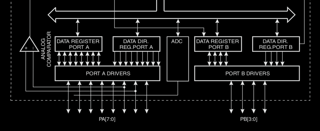
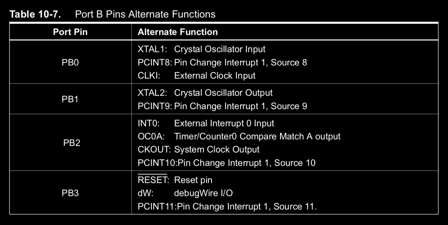
Port B (pb0, pb1, pb2, pb3) : 4-bit bi-directional I/O port with internal pull-up resistors (selected for each bit) : haha, i don't know what all of this means, but an 
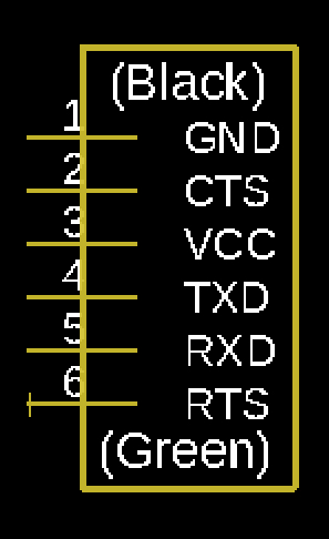
I/O port is an input / output device, which enables us to control the computer and display information in a variety of ways - many different kinds of ports can connect the circuit board to the computer, the most well-known being the USB port.

Maybe important to note, PB3 has RESET capabilities (which I don't know anything about), though you can program it to be another I/O pin. From neil's design, it looks like PB2 is one of the "free" pins which we will use to add an LED or button.
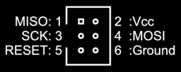
RESET : reset input. a low level on this pin for longer than the min pulse will generate a reset even if the clock is not running and provided the reset pin has not been disabled : apparently the reset pin used to monitor power fluctuations, when the power goes above / below thresshold volage, reset circuitry triggers an active low signal on the reset pin. Reset can also be performed to reset the state of the microcontroller.

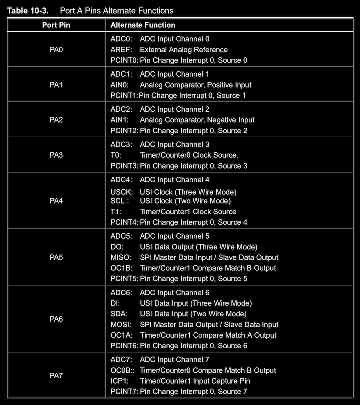
Port A (pa0, pa1, pa2, pa3, pa4, pa5, pa6, pa7) : 8-bit bi-directional I/O port with internal pull-up resistors (selected for each bit) As inputs, Port A pins that are externally pulled low will source current if the pull-up resistors are activated. The Port A pins are tri-stated when a reset condition becomes active even if the clock is not running :

so the description above is exactly the same as Port B, except that there are more port A pins than port B pins. I am truly not sure what "pulling low" means, but it seems like I just have to look up "pull up resistors" - more on that later. For now, I'm sort of wondering what differentiates Port A from Port B...

- - - - -

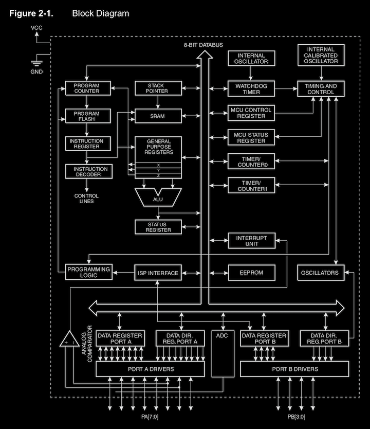
SO bascially, the ATtiny24A needs to receive power (VCC) and connects the circuit board to the computer via different / many I/O ports. (?!).

"block diagram" ???

this looks familiar

Again, I'm not sure what all of this is showing, but I can recognize the Port A with 8 pins and Port B with 4 pins.


ATtiny24 pin configurations :

Looking back at the pin configurations, I wasn't sure what everything in parenthesis is, but I gained some clarity by looking through the data sheet.

For example Pin 2 is labeled PCINT8, XTAL1, CLKI and PB0. This means that Pin 2 can be used as (looking now at the alternate functions tables below) Pin CHange Interrupt 1 (PCINT8), a Crystal Oscillator Input (XTAL1), an External Clock Input (CLKI), and Port B 0 (PB0).

port a alternate functions :

port b alternate functions :

- - - - -

neil's board's components :

neil's diagram :

At this point, I have a general understanding of what the ATtiny24's pins are, but I'm not sure why they are labelled as they are in Neil's board...

I don't know why the 2x3 pin header is connecting to specific points in the ATtiny.

I have no idea why the FTDI is connecting to both.

I almost gave up trying to understand the very basics of the echo-hello world and just start redrawing the board, which seems to have its own challenges.

I looked at various ex student's pages, but no one had a very clear explanation of what the board is doing. Most students seemed to just redraw the board, but I felt like I really needed to try to understand the board...

I basically wanted to find a pin out / data sheet for both the FTDI and the 2x3 header - seeing the pin out for the ATtiny was really helpful even just to conceptually understand. After much searching I found what I was looking for!

omg! ty batsocks for this 2x3 header pin out diagram :

The 2x3 pin out doesn't exactly explain why what is connected to what, but at least I now know that, like the ATTiny24, every pin is specifically designated.

Although I haven't found a pin out for the FTDI, I imagine one pin will be designated to VCC and another to GND... I mean, if we look at Neil's diagram, that is the case. Pin 1 is GND and Pin 3 is VCC.

Ok, so we've got some familiar terms : RESET, VCC, GND. Now let's learn about the other three strangers :

note : i'm now realizing, neil did talk about all of this in class, but clearly it didn't stick for me (altho the word problematic term MISO/MOSI did), so here i am wasting time trying to figure it out!

MISO : master input slave output : for sending information to "master" or data output from "slave"

MOSI : master output slave input : for sending information to the peripherals or data output from "master"

SCK : serial clock : the clock pulses which synchronized data transmission generated by the "master" or output from "master"

- - - - -

SO bascially, the 2x3 header is a programmer that allows you to communicate IN and OUT of the ATtiny - hence miso mosi?...


woohoo TY, FTDI for this informative diagram

After looking some more, I was able to find a pin out for the 6 way header (or what is labelled by many students as the FTDI, though that is the company that made this particular header? : future technology devices international... more confusionnnn!!).

neil's diagram :

If we refer back to Neil's diagram, this seems to match!

Again, I still don't know what is going on, but I feel better knowing that the ATtiny, 2x3 header, and the 6 way header all have assigned values that mean specific things.

6 way header pin out :

So lets learn about these unknowns :

CTS : clear to send control input / handshake signal : CTS and RTS allow the receiver and the transmitter to alert each other to their state. A transmitter raises its RTS line, which causes an interrupt on the receiver : hi, can i send some data? If the receiver is in a position to receive the data it will assert its CTS line : yes, you can start sending.!

RTS / CTS flow control : the raising and lowering of these lines allow device drivers which implement hardware flow control to maintain a reliable data connection between transmitter and receiver.

ty, brainboxes for this explanation!!!

TXD : transmit asynchronous data output : transmits data (seems like opposite end of this would be an RxD) :

This means that RxD must be an in- put on one device and an output on the other device. Thus the terms RxD and TxD do not say whether a pin is an input or output but are instead names for pins on the connector. (thaaaanks, electrical and computer engineering at UBC!!!

RXD : receive asynchronous data input : receives data (seems like opposite end of this would be an TxD). See above!

RTS : request to send control output / handshake signal : refer to CTS above!

- - - - -

my "aha" moment :

so all main components : ATtiny, 2x3 header, and the 6 header have both VCC and GND and in Neil's board, he seems to connect all of them.

Then, is it safe to assume the left over ATtiny pins just need to connect to both 2x3 header and 6 header? So if you needed to connect to less things you could get a smaller ATtiny, and if you needed to connect more, you would get a bigger one?

In neil's board, then, PB2, PA7, and PA3 seem to be "free" and is where we could connect the LED and button?

looololol - I'm truly not sure, but I think I feel comfortable enough to start heading into KiCad and/or Eagle.

- - - - -

components laid out in Eagle :

A total of 08 components :

01 : ATTINY44 [ATTINY 44-SSU]

02 : FTDI HEADER [FTDI - SMD - HEADER]

03 : AVRISP SMP [AVRISPSMD]

04 : RESONATOR XTAL 20 MHz [RESONATOR]

05 : RESISTOR (10k) [RES-US1206]

06 : CAPACITOR (1F) [CAP-UNPOLARIZED]

07 : BUTTON [6MM_SWITCH6MM_SWITCH]

08 : LED [LED] + [RES-US1206]

a big shout out to rafa's electronic design week for the helpful instruction!!!

ATTINY44 Schematic :

FTDI HEADER Schematic :

AVRISP SMP Schematic :

RESONATOR Schematic :

RESISTOR Schematic :

CAPACITOR Schematic :

BUTTON Schematic :

LED Schematic :

rafa's schematic :

my schematic : lol

I followed Rafa's page in order to organize the schematic. I was confused by why I was connecting every single thing and he didn't have to... I realized he was NAMING things and naming things connected them if you did it all correctly (which I did not do - hence my mess of a schematic).

board on Eagle : idk not bad

Going from schematic to board was stressfullllll. Everything was criss cross all over the place. My OCD couldn't handle it. I linked and relinked things over and over again in schematic version.

I did end up finding it easier to slowly build the schematic and simultaneously route connections. Routing connections allowed you to begin to place things logically, rather than have wires go across the board in a really annoying way.

After I had everything more or less in place, I was able to tighten the board. My goal was to make it as small as possible - which I hope was not a bad decision. I guess, if you had more space, it might be easier to solder. It measures about 2" x 2".

trace ready to mill : *love the unecessary squiggle on PA5 / MISO

I made sure to add some space to the right of the FTDI - Neil mentioned you didn't really want this guy hanging off the board.

If all is well, this board should work?...

- - - - -

board 2x larger :

I started milling my PCB and realized my board was 2" x 2", but most of the copper stock was no bigger than 2".. I asked Jen if there was any larger stock, but she mentioned my board seemed quite large and asked whether I had spread things out. Quite the opposite, I had tried to make everything as compact as possible. She suggested I scaled things to be half the size, so I did. I had read on Dalma's site she also had a similar issue, so I wasn't surprised, but I am curious why my board was exactly DOUBLE the size, vs, idk, a quarter? Or some other arbitrary percentage?

making sure scale is accurate

After I milled the traces, I grabbed a 2x3 header in order to see if the scale was correct. It seemed like it fit perfectly into its footprint, so I went ahead and milled its outline.

traces merged footprints :

Thankfully, I had looked at a lot of student's electronic design pages, so I knew it might be possible for my pcb to be milled incorrectly - in particular, a handful of students had the reset pin merge into the leftside of the ATtiny. This happened to me too, but all I did was cut the traces where they didn't belong with an exacto knife.

trimming the bad trace:

I tried my best to do this as clean as possible. I'm not sure if this was enough to correct the problem.

finished soldering:

Soldering went pretty smoothly - this time I used the magnifying glass.

unsuccessful programming:

However, when I tried to upload Blink via Arduino, there was no blink!

By the way - in order to use arduino, there were a couple of steps involved : explained HERE.

To be clear, I had multiple errors : my USB programmer was not being recognized, I was using the wrong board, or the wrong programmer, etc.. But finally, I corrected all of those things and Blink successfully uploaded without any errors, but there was no blink.

I will be trying to meet w a TA Tuesday morning to try to see whats going on. I hope I didn't mess anything up too badly.

- - - - -

pin no. different in arduino :

It turns out, I was assigning the wrong pins when uploading via Arduino. I was relieved it wasn't somethign wrong w my board. However, when Diego and I tried to re upload to the board w the correct pins assigned, we were met with a series of errors. Neither the programmer (ICE) or the programmer I had made in WEEK 03 were being recognized - the usbtiny seemed to be the issue, not my programmer. When I met with Anthony for office hours, he was able to upload Blink to my board on the first try. Super frustrating...

Anthony did notice my LED was quite low, and that was because I used a really high resistor (100). He also mentioned I was missing a pull up resistor for my button, but I had read in Rafa's documentation that after he did a ton of extra outside wiring, he was told he could have just altered his code - so that is ultimately what I decided on.. I was happy I didn't have to pull apart my board!!

this is the code I used (which was written by JACLYN)- notice the PULLUP that creates an internal pull up resistor (not in her original code, but mentioned by Rafa) :


In general, I enjoyed this week. I do hope to gain a better understanding of electronics, though the workflow from eagle to programming seems manageable and not so scary anymore.