Work Progress
This week's task is to use a desktop milling machine to produce a circuit board already designed.The first step is mill.
Since this is the first time to use this machine (although the srm20 is very small compared to lasercamm), I was very afraid
that I would break the tool due to an operational error, so I summarized a detailed procedure in advance. However, the whole
process is not very smooth, because I don't know why every time I move the tool to origin, adjust the length of the tool, and
send file to machine, I will get the prompt of object blob and the machine will not respond for sure. To keep it working and
stop complaining, I had to restart the machine every time I use a new tool.
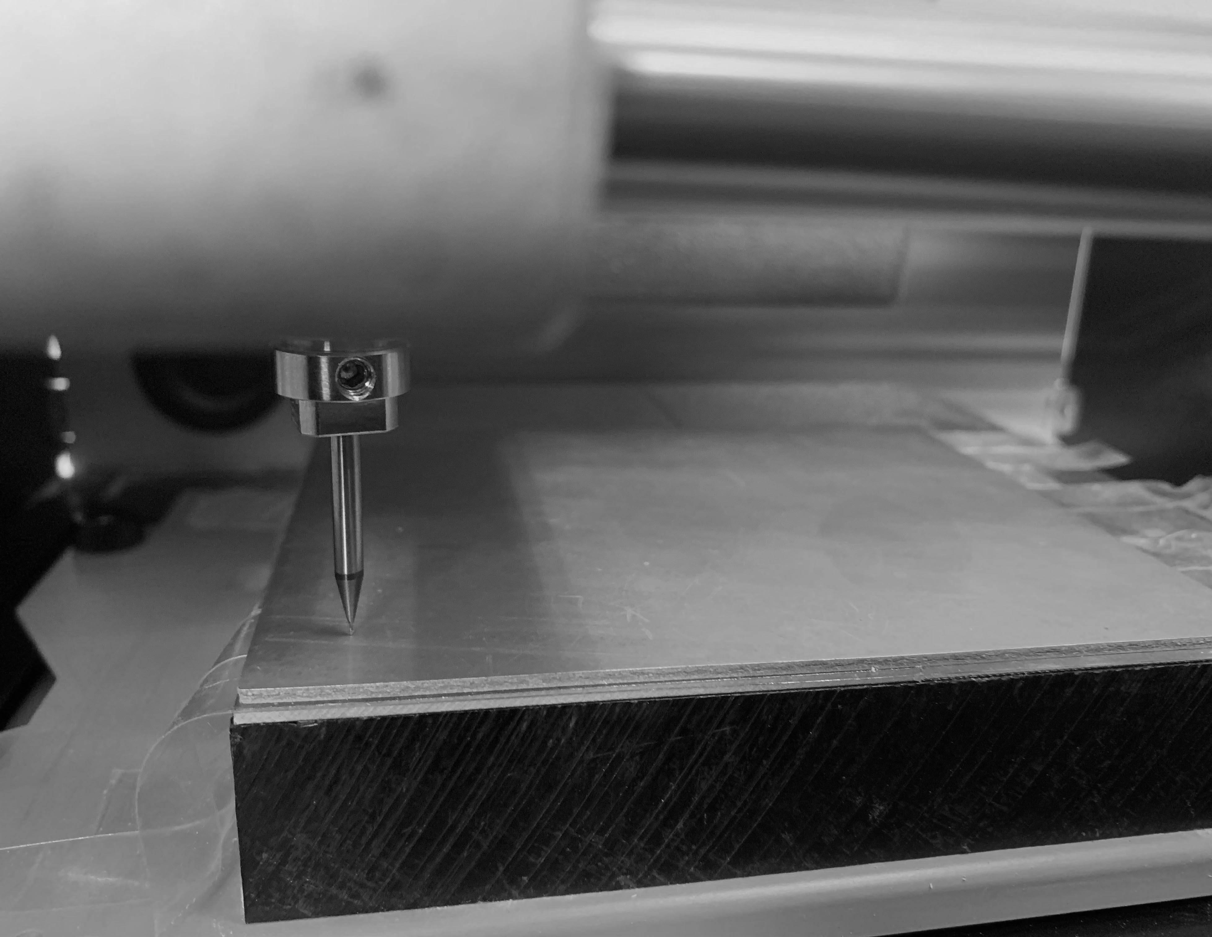
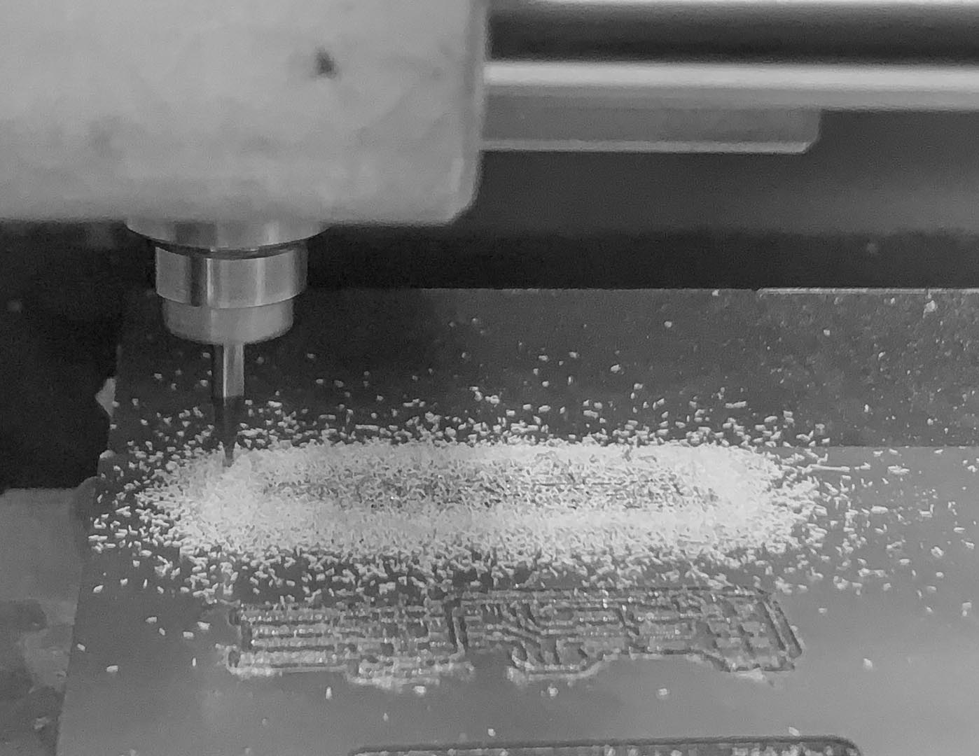
The following is steps and precautions I summarized:
After I finished mill, the second step is finding components. Here is a list of components we need for the board:
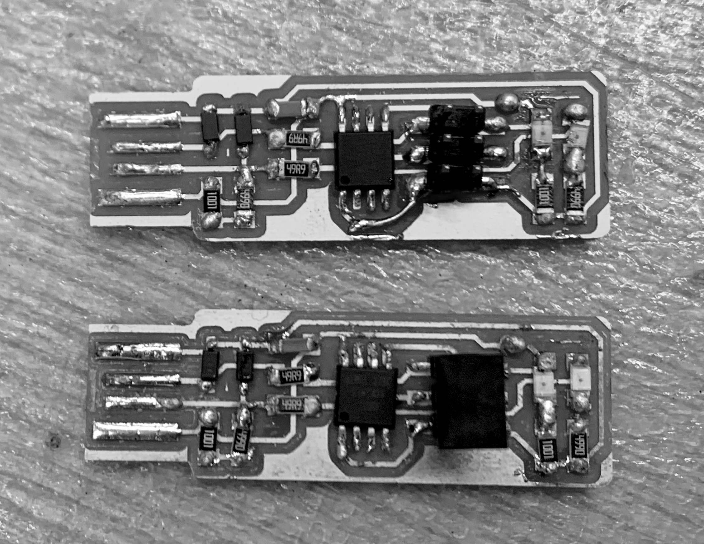
I not skilled for soldering that I never had soldering experiences before, not to say soldering such mini components. While Paloma showed us the soldering process, it looked very simple and each joint glittered, however, it was totally different in my own operation. Even though I did a lot of practice on the discarded PCB in the shop table, I was completely stranded and only able to complete one circuit boards after a total of 3 discarded milled boards because I couldn’t unweld. The shape and appearance of each joint was not good.
Update from mid-semester: Soldering is one of my favorite things to do in a week(compared with programming). I've enjoyed it after I practice myself a lot. I've summarized a written version of the procedure:
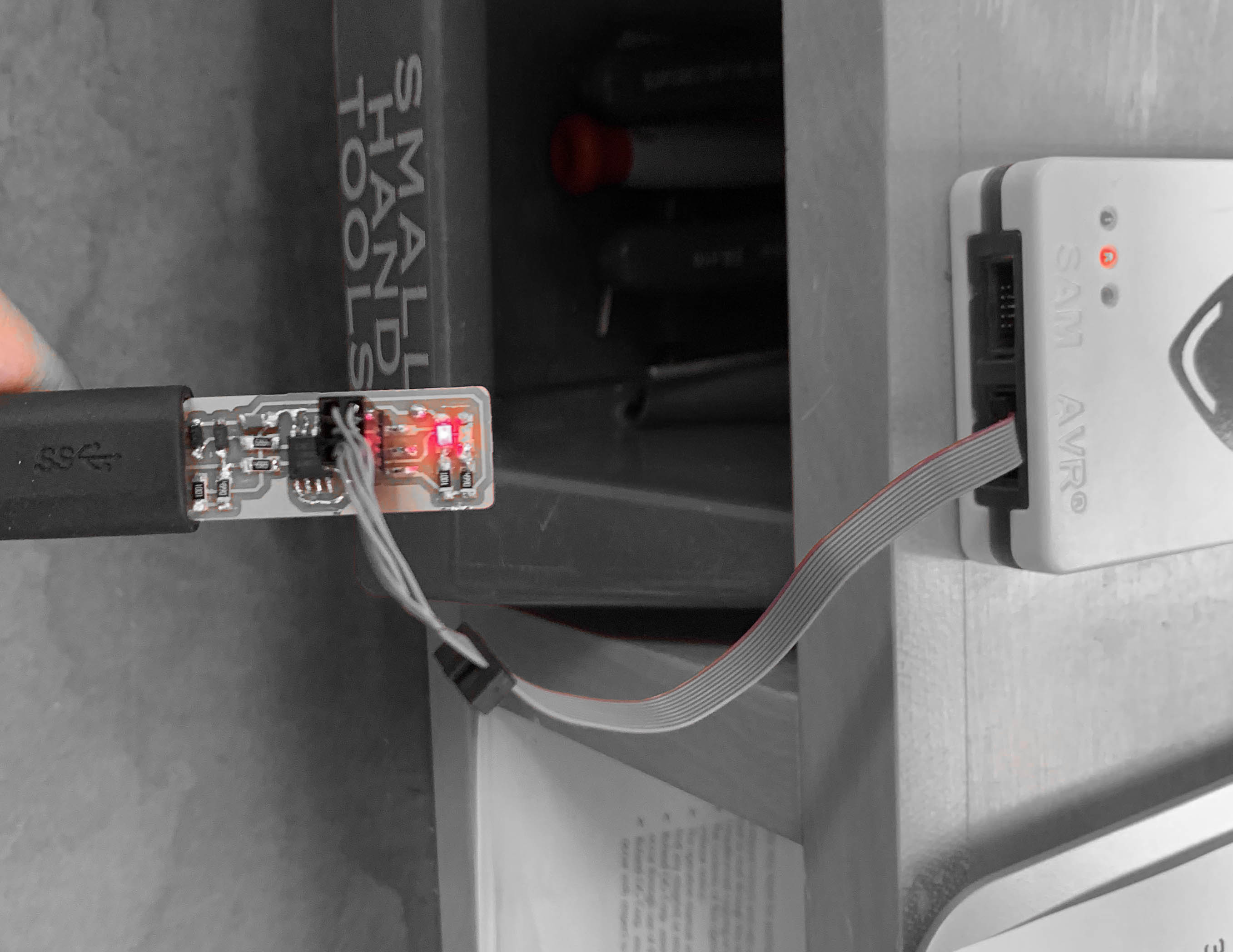
Because of the poor quality of my solder, I could not successfully program it, so I went to Anthony's office hour. Anthony found that one of my components had become warp, which caused the short circuit.
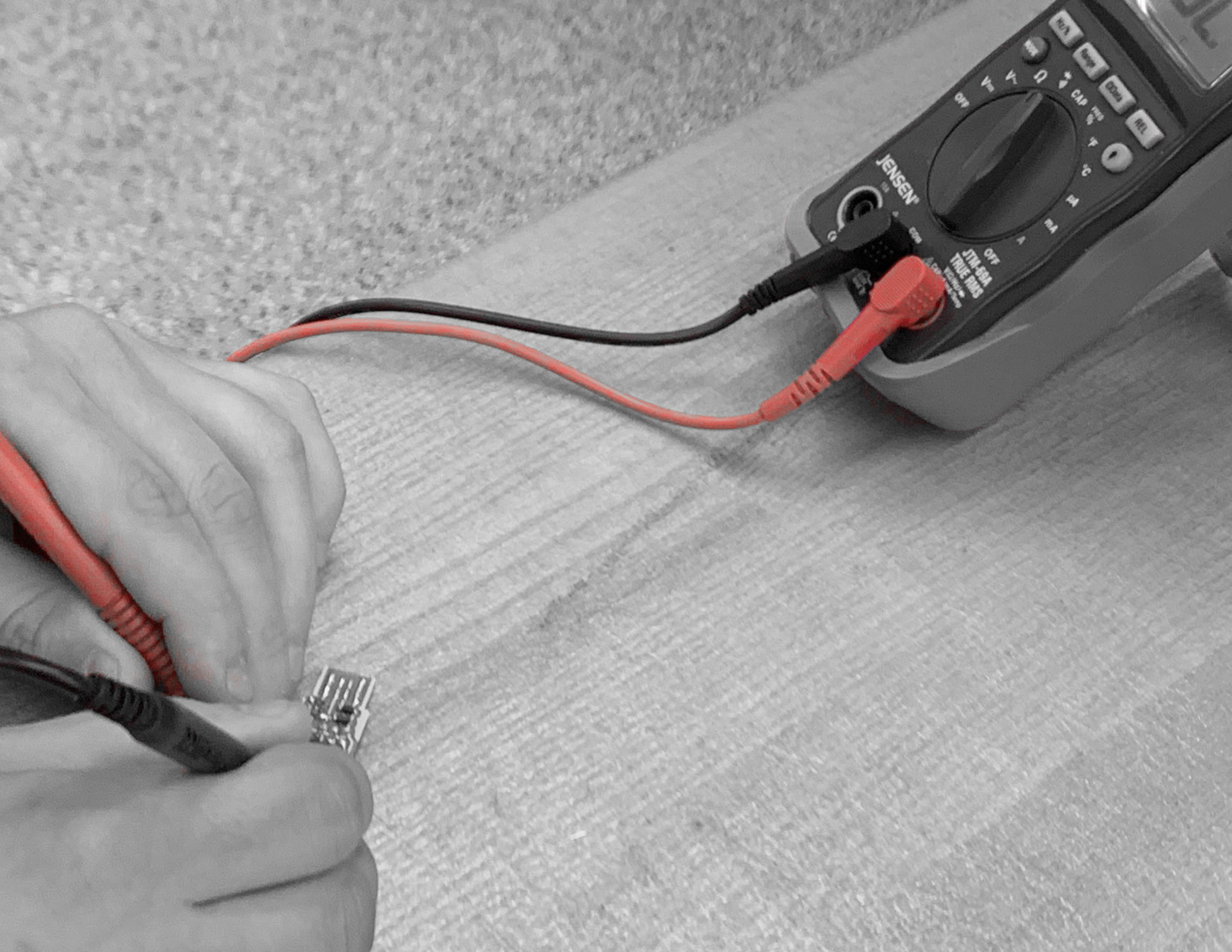
He taught me how to use the multimeter to test the short circuit and the unweld technique, and finally I was able to successfully program it!