I want to make a speaker. Something that can eventually synthesize and play a whole song on achip - like this project from Brian Mayton. that might not be the outcome of this week - but I'll need to have something more advance synthesizing instruments and music by the time of my final project.
Neil's helloworld board breakdown
The helloworld speaker example that Neil has is basically a ATtiny45 hooked up to a N-channel mosfet and speaker. In class, Neil described the NDS355AN and NDS356PN as "life-changing" parts - so let's dive in to what they are / what they can do.mosfet (metal-oxfide-semiconductor field-effect transistor) is a transistor part with three terminals - source, gate, and drain - the voltage applied at the gate determines the conductivity accross the source and the drain - which can be used for amplifying to switching electronic signals. mosfets transformed the elctronics industry after their invention in 1959 because they were cheap, requried no input current, and were highly scalable with moore's law. There are p-channel mosfets and n-channel mosfets made out of p-type and n-type semiconductors respectively {{quick solid state refresher: p-type semiconductors - doped with electron acceptor atoms, majority of the charge is carried by Positive holes, fermi-level below intrinsic and closer to valence band. n-type semiconductors - doped with electron donor atoms, charge carriers dominanted by electrons, fermi-level above intrinsic and closer to conduction band}}. in an n-channel mosfet, the source is connected to ground, the drain to the load, and when a positive voltage is applied to the gate the fet will turn "on" - these are easier to work with and cheaper to buy. in a p-channel mosfet, the source is connected to a postive voltage and the gate will turn the fet on when it's below the source voltage by some amount - these are harder to work with because you need another transitor to turn it on and off if you want to switch voltages higher than 5V. MOSFETs also appear to come in either enhancement mode or depletion mode - in enhancement mode applying a votlage will turn on the transitor, depletion mode is normally on and an applied voltage will turn it off.
Neil's speaker uses the n-channel enhancement mode mosfet - datasheet here.
design board
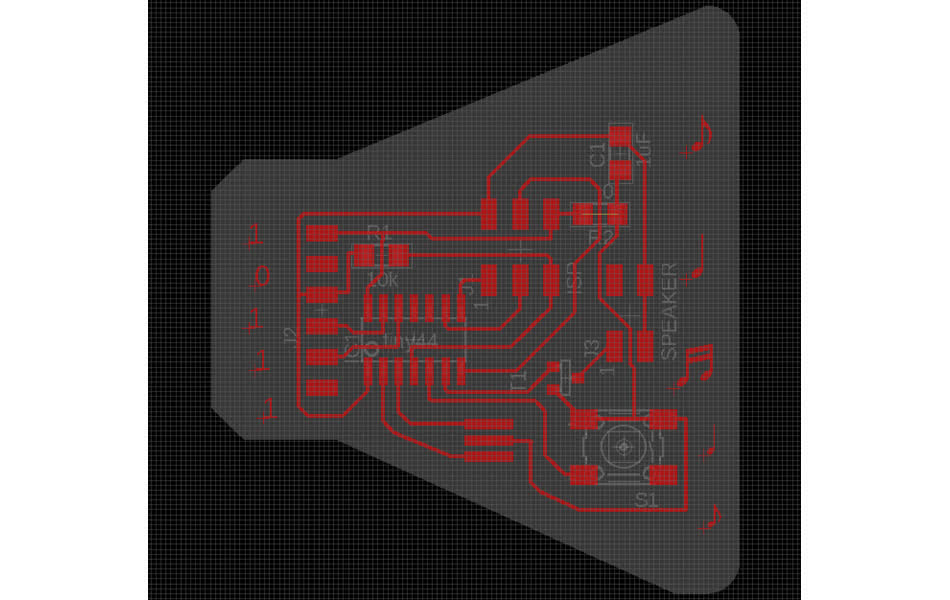
I'm going to make basically the same baord as week 4, but replace the LED with the n-channel mosfet and speaker. I'd like the speaker to make noise both programmatically and with the button. To allow the timer to control the mosfet {{thank you for the tip zach!}}, I made sure to hook it up to a pin that has access to the timer - these are any that say OC. I'm not super worried about the volume of the speaker - so insetad of having an external power supply with a reguulator powering the speaker (as is the case in neil's board), I'm pulling power from my laptop with the FTDI connector and can get rid of the 5V regulator. resitor is a pull up resistor for the reset button.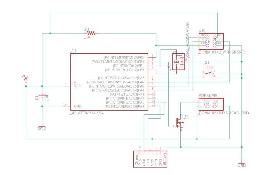
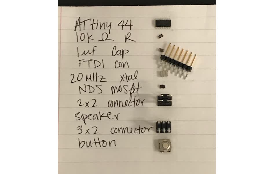
Now that I have the generual concept and design of my simple speaker board, I'm going to check that we have all the parts before investing time into designing with all the components.
It looks like I should be good.
Time to do the actual board design
I still can't figure out how to get the eagle_png.py script to output pngs with a border, or atleast to follow the polygon cutout made in the board instead of the one made on the milling layer?? I want to look more in to the script if I find the time.
but in the mean time, I add a 50 pixel black border to both images with this online tool.

Then, I need to calcualte the dpi to set in mods to make sure that the board comes out the proper size.
eagle measurement from button ground pad: 2.3mm ~ 0.09 inch
imageJ to measure button ground pad in pixels: 273 px
therefore, dpi = 3033
The traces didn't come out well - some were not cut out all the way. I think didn't imported the design rules properly - I had a feeling something was off when I made the board because I felt like I could bring the traces much closer than I had on previous boards.
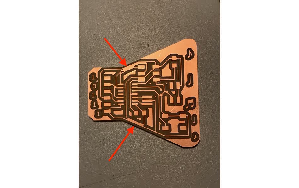
Looking back at the design rules, everything seems to be setup corrently. when I run the design rule check there are no overlap errors, but when I turn on the grid and look at the distances, they clearly violate the design rules. I'm not sure where the issue is coming from - maybe the rules are only being enforced on certain layers or something?
Since I couldn't find the source of the problem (even after redownloading and loading the design rule file from here), I increased the space minimum to 18 mil and turned on the grid with 16 mil boxes so I could manually check the distance between each trace I was drawing.
I spent another hour and half trying to redesign the board. The longer I looked at it, the more problems I found with the milling and cheating corners with the trace/space boundaries - I don't know why Eagle isn't automitcally picking them up.
I kept running into the same problem with diferent parts in different positions - basically I have voltage and ground going along the outside of the circuit and there's always a point where they need to cross each other. I tried to continue changing orientations of different parts, but it's 2am on tuesday night and Zach showed me a trick to use a 0 Ohm resistor as a jumper to hop a wire so I'm going to give up on single layer PCB purity and move forward with the jumper resistor.
I added a 0 ohm resistor connected to ground and ground in the corner of the schematic and redesigned the board
Then exported new png files
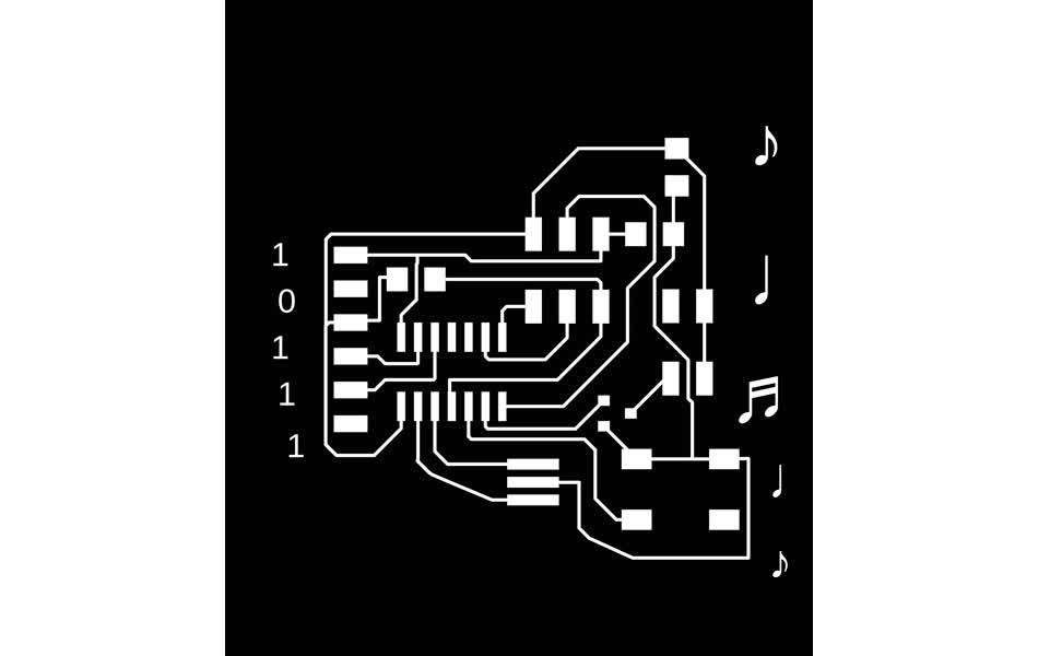

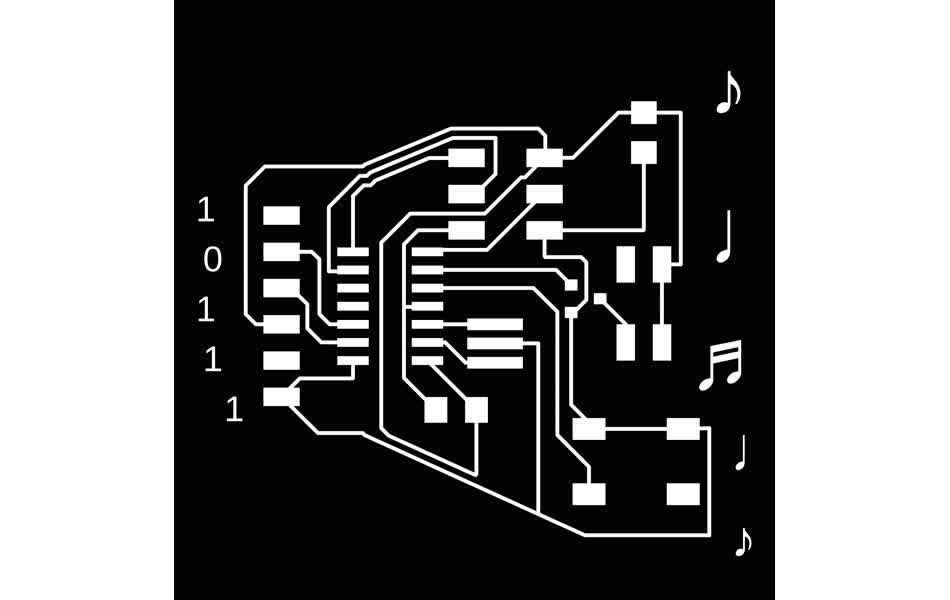
It worked!!
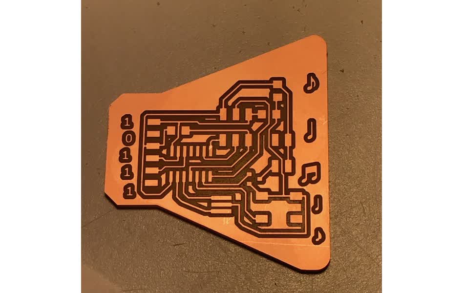
time to solder

soldering came out nicely. I quickly tested that the voltage and ground lines with a beep test on the multimeter and everything appears to be connected well.
Programming
I want to understand how to program the AtTiny44 to be a speaker from scratch. I'll start by taking apart Neil's helloworld speaker for the tiny45. . .Neil's makefile first generates the .hex file which will be sent to the target board and then has the avrdude commands to actually send the code.
avrdude commands
-
-p: part number, tells avrdude which microcontroller its programming, ex t44 or t45 -
-P: the communication port to talk to the programmer. usb in our case. -
-c: specify programmer type. Neil's makefile has lots of different options. I'm using the one I built in week 2 which is usbtiny. -
-U: input > memtype < : r|w|v : > filename < [:format:]. main flag that actually does the programming. memtype can be flash or eeprom (electronically-erasable programmable read-only memory). r:read, w:write, or v:verify. filename you want to read or write from - in this case the .hex file. and fianlly the optional format flag - .hex is "Intel hex" so it could be set to "i".
I added an external crystal for timing on the speaker so that it could be more accurate - but I need to reprogram fuses to look for that. I put the crystal on the same pin as week 4, so I think I can copy Neil's lfuse command from AtTiny44 helloworld.
mirroring Neil's attiny45 speaker helloworld for my attiny44 board . . .
#include :: includes header file that has all the IO definitions for whatever device was specified in -mcuu compiler line.
#include :: needs the F_CPU macro defined ( this is done in Neil's makefile) - it's the CPU clock frequency for the controller - potential play with this value so it matches the xtal??.