Week 8: Input Devices
Summary: I had a fruitless time this week trying to mill a board for an ADXL343.
A new board, a new hope
I made a new board, routed it all by hand. Maybe someday
I'll look into SVG PCB.
I kept on second guessing and wondering if I should add functions like a speaker to create the whizzing noise now or if I should find a breakout board accelerometeror not. I ended up having pinouts for a speaker and tried to do the surface mount accelerometer. Keeping spiral development in mind, I had ready access to the surface mount ADXL343 and learning how to attach those would be useful, and I could experiment with the speaker if I so desired.
Another thing to remember is that for a two sided board, the outline should be symmetrical so you can turn the board over and it'll still fit in the cut-out within the full copper board piece. This is critical to keeping the "home" position the same. Also don't forget to mirror the trace.
Files: trace.png | trace.png | trace.png | trace.png |
Note: These are faulty since the ADXL343 is missing components. More on this next week.


Fabrication
You just love to see this happen **bleeds sarcasm**
Anyways, that wasn't the only issue I had. It is impossible to figure out the exact placement of this board again, and maintaining the same placement in important for making sure the back traces lines up with the via holes. I got a new stock and tried again.


Two sided board mishaps
The traces for the ADXL343 needed to be TINY. I didn't trust the larger end mill, and used the 1/100" one. I forgot to fix the depth settings however, and it cut wayyyy to deep the first time. It was perfectly aligned though! However, as I couldn't really "re-do" just the back side without redoing the front, I decided I'd just solder wires for the sake of time.
But for future's reference, I decided to try other milling sizes on the unused board space.
You'll also notice a trace of my board on the back. To be an upstanding lab-user in conserving copper board stock, I decided to re-use the double sided board since the backside needed much less space.
But for future's reference, I decided to try other milling sizes on the unused board space.
You'll also notice a trace of my board on the back. To be an upstanding lab-user in conserving copper board stock, I decided to re-use the double sided board since the backside needed much less space.


A Few Days Later...
While I planned for this week's board to sustain the following couple week's worth of programming-based projects, I was not able to fully get a sensor working this week. I decided to document any sensor-related efforts in the coming weeks here.
A couple days into fiddling with the board I ade this week, I realized, while looking at Neil's documentation, that I needed a new board. This was done and documented in week 9.
A couple days into fiddling with the board I ade this week, I realized, while looking at Neil's documentation, that I needed a new board. This was done and documented in week 9.
Crash Course in Reflow at EECS
After vocalizing my woes in class the following week, Anthony offered a reflow office hours at EECS. I joined and brought in my monstrous board from week 9.
My two-sided board was misaligned and several the traces on the back did not connect where they should. Also, being a double sided board, the hot plate method I used before does not work. You can't even lay it flat once you have a single component on the opposite side, which was poor planning on my part.
He had a pretty cool demo on reflow. Main takeaways:
- remove anything that could lead to a short circuit - clean off any pulled-up edges, remove any specks of copper between traces, etc.
-- holding a 1 sided board to a light can help identify connected traces - 270-330C heat for a board (using a hot air reflow gun)
-- But exposing the board to low or mid 200C temps for long durations is bad for it (copper will bubble - which has happened to me with the hot plate!!) - 30% airflow, Hold it at 90 degree angle
- Wicking is best with a soldering iron at 600F+
-- wicking is often a heat transfer problem, usually when they don't work, it's too cold or the soldering tip is oxidized. Can add flux/solder as well - Solder paste will stick to the copper when heated, and should be completely shiny
- Components floating on solder paste can place themselves in the proper orientation as the flux evaporates as long as they are less than a half pad away from where they should be. Just tap them as they're floating on heated liquid solder
- Oftentimes, to seperate excess solder blobs, heating the blob and making a swishing motion away from the connection with a hot iron can help


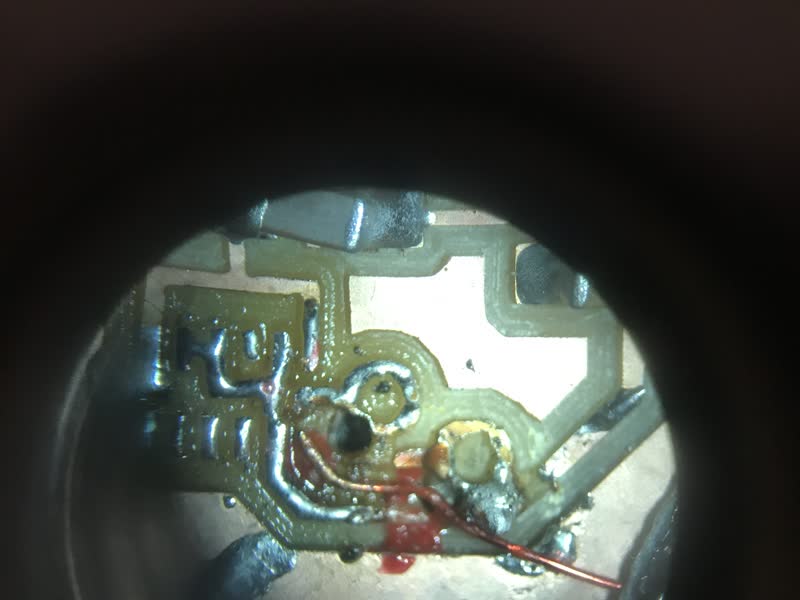
Surgery
In trying to fix the disconnected traces on the back of the board, I also got help from one of my hallmates, Anhad, and we
did what felt very close to surgery on the lil guy.
One thing that occured was a trace pads at the end of the accelerometer ripped completely off, and one solution was to dig out a little recess under it, then stick a wire there that could be soldered directly onto the accelerometer's pads. It was an ambitious undertaking. It required the use of a microscope!
You can see some very small wires used. The tiny copper one is wrapped in clear insulation I had to melt off obeforehand on the tippity tips to connect. The red stuff is a heat activated expoxy adhesive that is non-conductive. The wires wrap around the other side of the board.
But regardless of the hours spent, the ESP32 still wouldn't recognize the I2C connection. :(


Eventual success
I decided that there is so much that can go wrong with soldering a surface-mount teeny accelrometer. I don't even know if my related circuitry for the ADXL343 was correct or not. I also don't know if I've fried it by now. I decided to look into breakout boards that come with the related circuitry and just have pinouts.
It also came to attention from my friend Winnie that the ADXL343 doesn't capture data up to the forces that I would be exerting on it as a spinning prop for my final project.
Finally good news: For my final project, I was able to read accelerometer and gyroscope data that was connected through a breakout board!!! However, I wasn't able to do much because I soon after ripped the traces connecting to the power.