Week 3: Electronics Production
Assignments
This week’s individual assignment was to make an in-circuit programmer that includes a microcontroller. I chose to make the “hello.D11C.serial.5V.1.1” PCB that uses a 14 pin Atmel SAM D11 microcontroller.
This week’s group assignment was to characterize the design rules for the PCB process. We used a trace with channels and ridges of magnitudes between 0.001 and 0.20 inch to investigate how well a 1/64” bit could mill. The bit was unable to penetrate areas with channels <.016 inches, but was able to mill around the ridges somewhat successfully. The details of the group assignment can be found on Doria and Niccolo's sites.
Milling and Assembling a PCB
Milling with the Roland SRM-20
I began milling the board by uploading the trace and outline to the milling software. I began with milling the trace first with the 1/64” drill, but the trace was not clearly engraved at first, so I stopped the machine, waited 5 seconds(something I forgot to do many other times), and then loosened the drill bit to force it onto the surface of the board so that it would engrave deep enough. I then cut out the board with the 1/32” drill, which went fairly smoothly. One important aspect I remembered was to remember the coordinates for the origin, as I ran into the problem where the coordinates reset before cutting, meaning I was at risk of cutting through my traces.
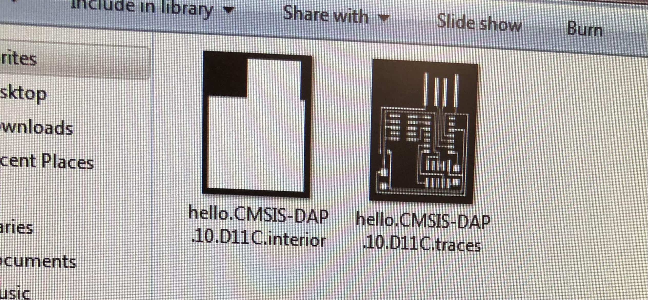
Figure 1: These are the files for the trace and interior of the PCB.
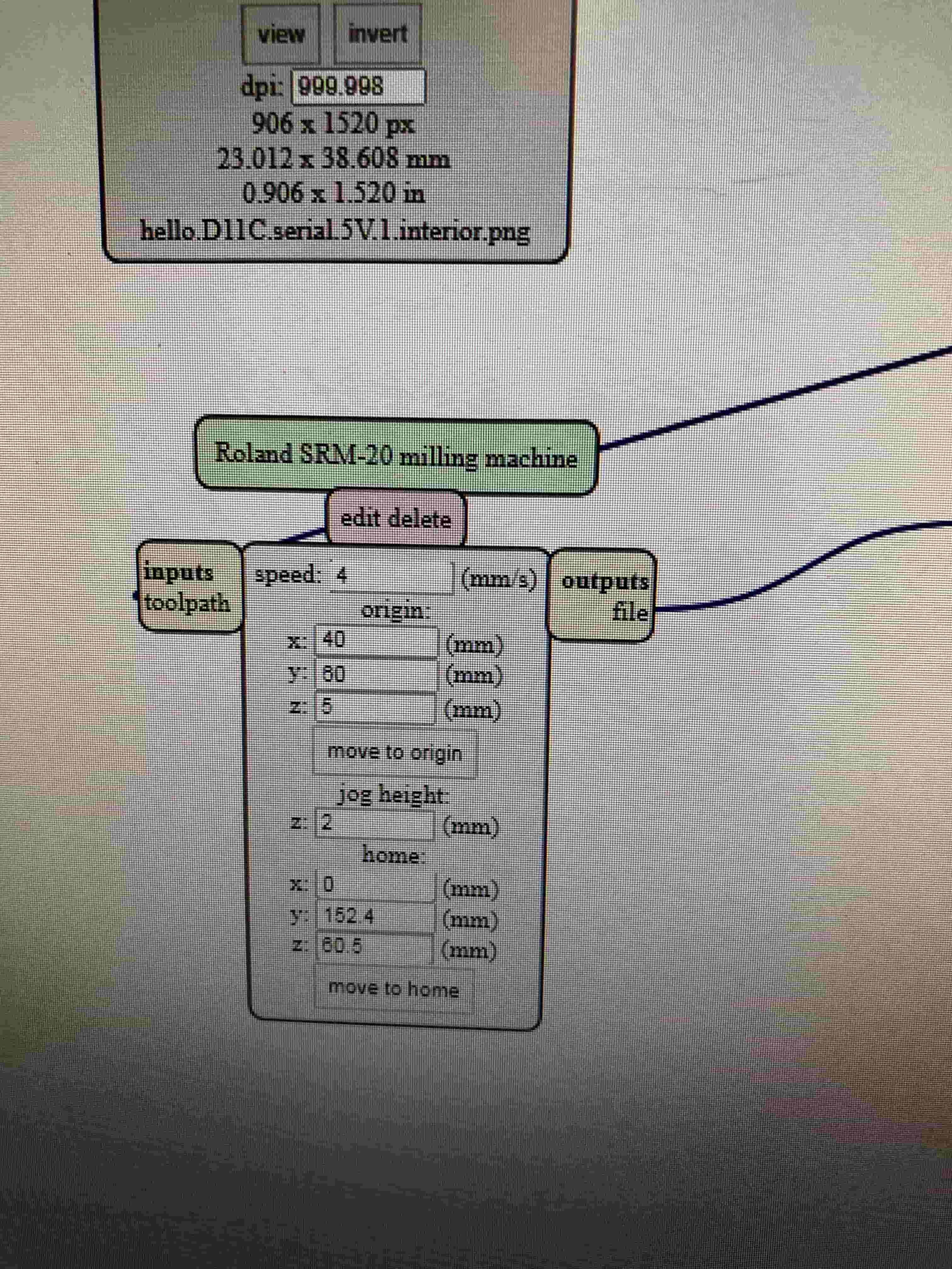
Figure 2: Using Neil's mod to customize origin coordinates.
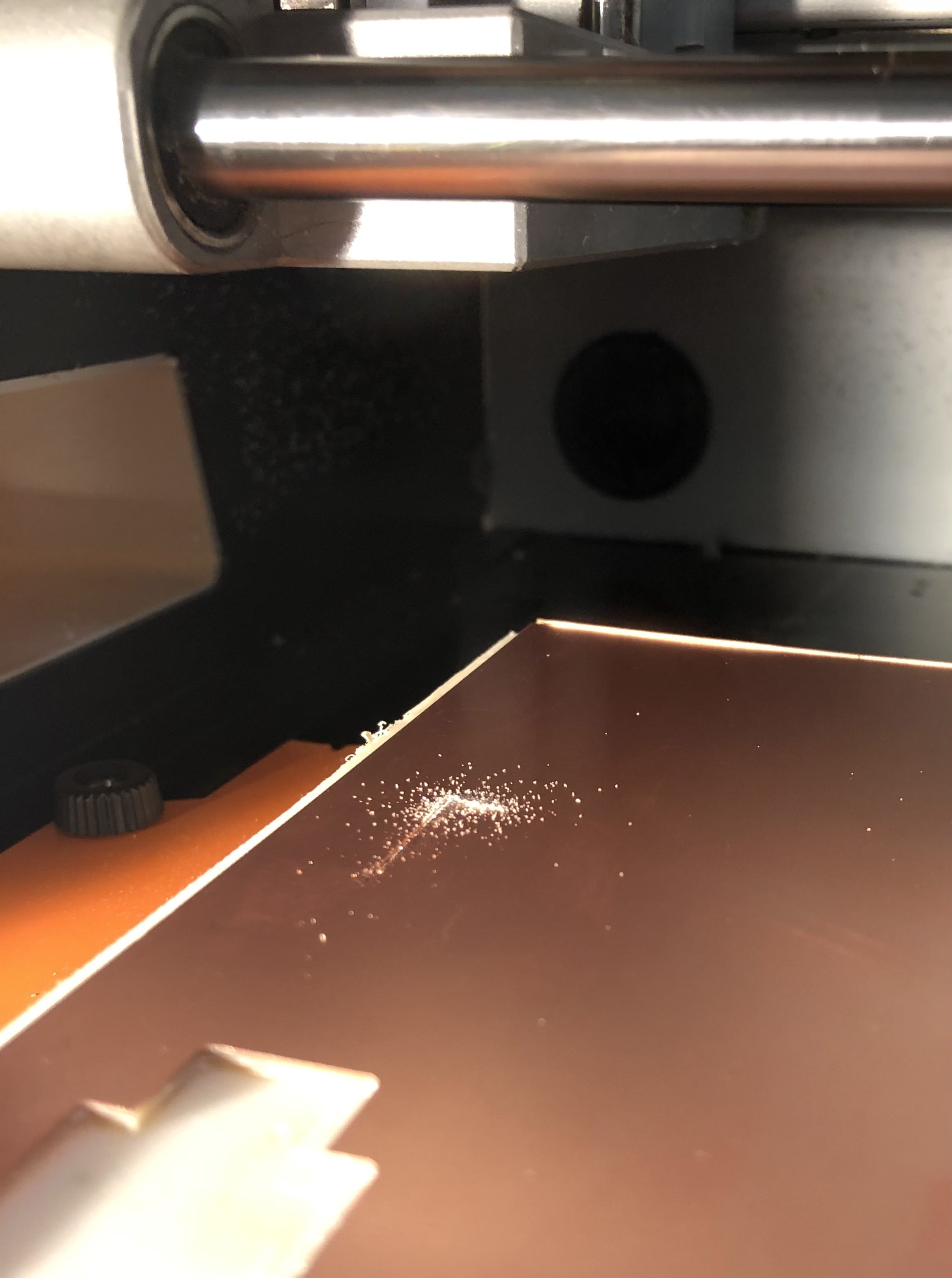
Figure 3: I had to stop the mill because it wasn't drilling deep enough, which was evident by the lack of white builldup.
To prep my board for soldering, I sanded down my board because the traces were engraved somewhat roughly, which I could attribute to the drill bit giving out by the time I could mill. There was also a strange residue on the traces(possibly from the sandpaper), so I cleaned the surface with alcohol, and it looked ready to solder.
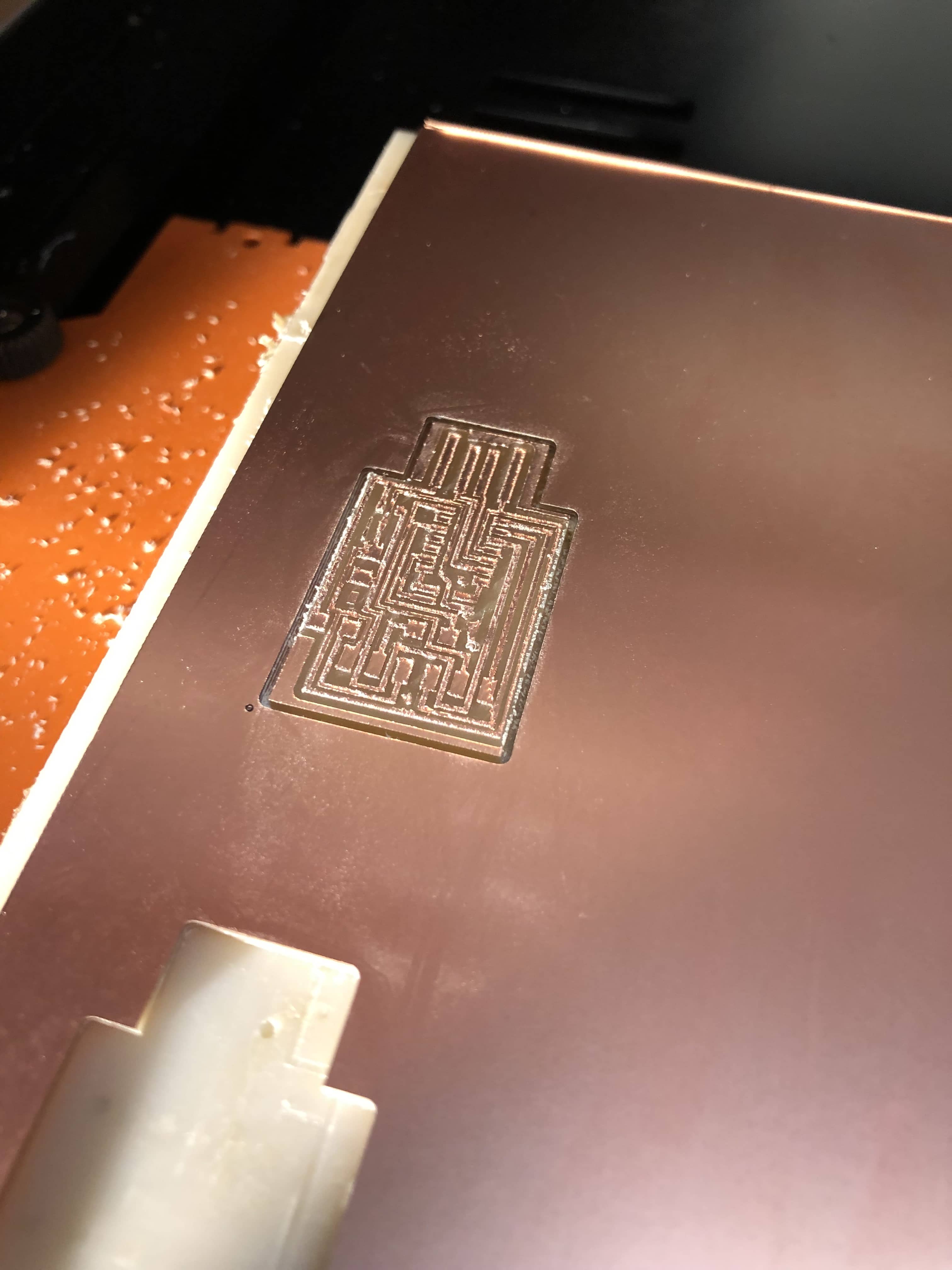
Figure 4: The traces seem to be peeling and the edges looked a little rough, but nothing a little sandpaper can't fix.
Soldering
Before soldering, I gathered the parts together and labeled/taped them onto a piece of cardboard. I then gathered my supplies for soldering, including the solder iron, vacuum, microscope, soldering braid, sponge, and tweezers.
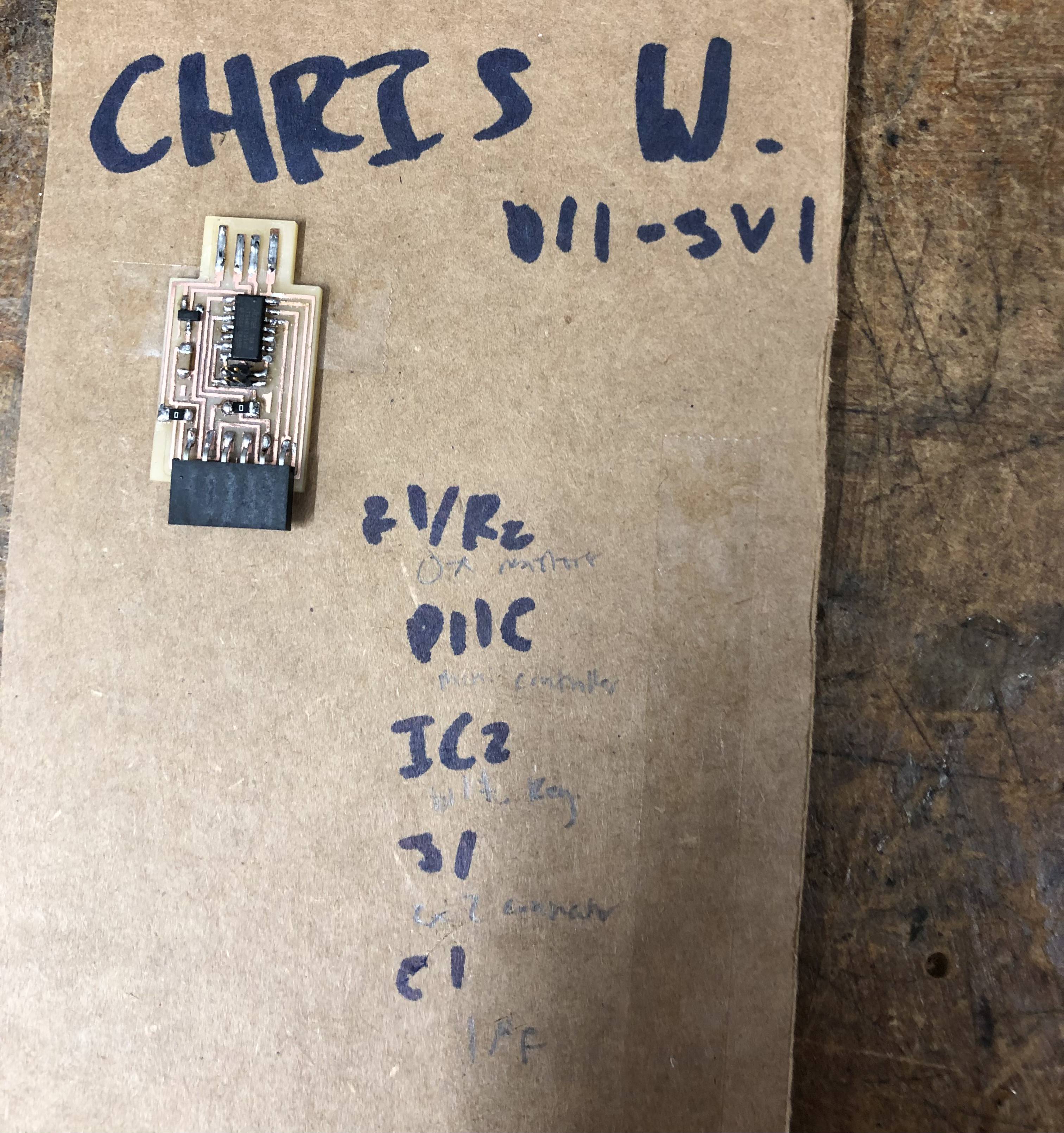
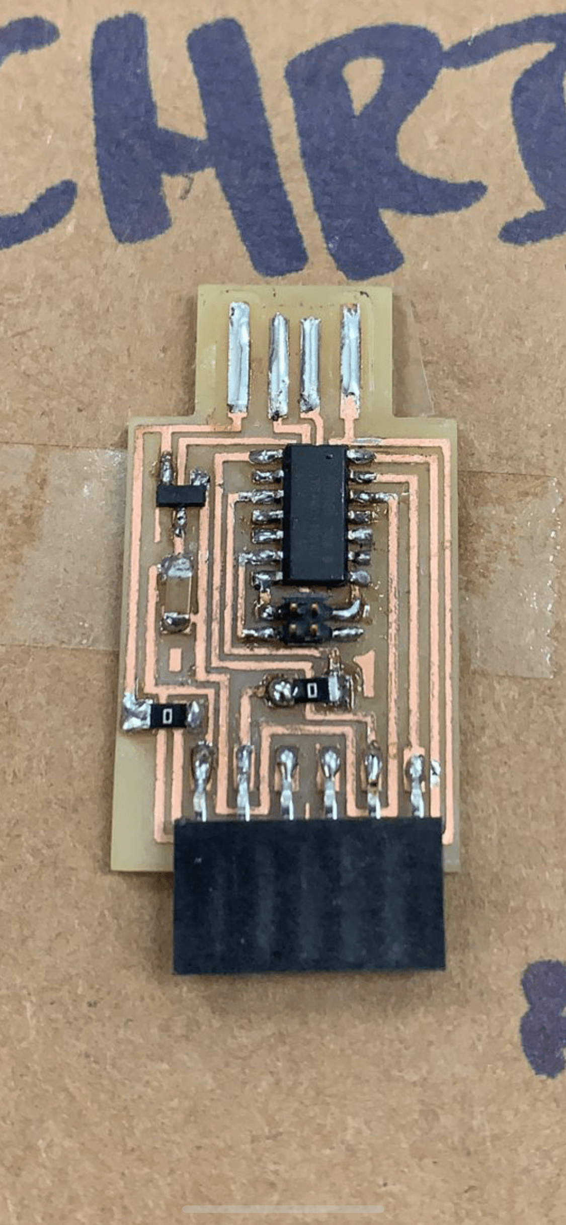
Figure 5: I became too determined to solder so I forgot to document all my parts on the cardboard, but left the labels.
I did not find soldering too difficult, but I was definitely frustrated before I mastered the technique of touching the solder to the surface the iron was already heating up closely. I made a couple mistakes where I soldered too much onto a different trace, but I removed it with a soldering braid. Eventually, I finished without burning myself, and my soldering looked decent enough for the PCB to be functional. I went back to clean up my end traces because they weren’t smooth enough to insert into the USB port.
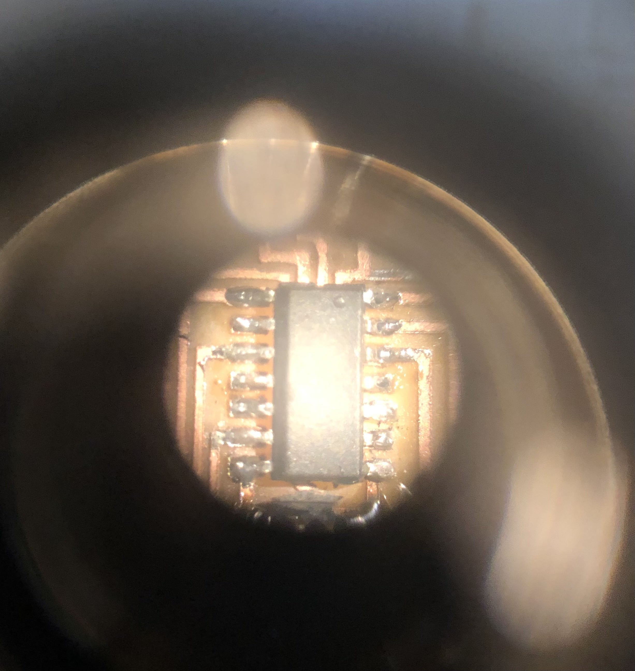
Figure 6: This is a photo of my microcontroller being soldered on through the microscope
Testing the Board
I came in on Monday night to test my board with Rob. We used a digital multimeter to measure the voltage at different points on the board, and referred to the board graphic to ensure that the values aligned. Success! Every part of the board we tested was either 5V or 3.3V, so my PCB was confirmed functional and ready to program.
If I were to change anything about this week’s assignment, I would find ways to customize my board. This could be as simple as cutting out a different shape with the same trace, or even changing the paths of the trace to make a design, but for now I just wanted to make something that worked.