Topics
Semiconductor Device Modelling
Theory
This work limits to pn-junction/mosfet and all material properties is assumed.
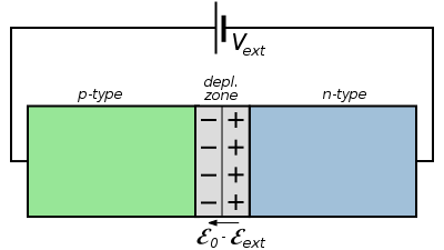
pn-Junction
Analytical vs Numerical
Boundary Condition
Vmax = 1.0; % max voltage for voltage sweep
Vmin = 0.0;
Drift-Diffusion Model
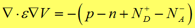
Non-linear Poisson's Equation
- Neglecting Magnetci Filed
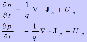
Continuity Equations
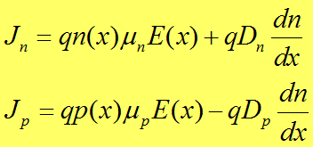
Current Density Equations
Solving Poisson's Equation
- Finite Difference
- Finite Element (used in this work)
Galerkin Method: 1D Poisson's Equation [3]
Numerical Integration: Gaussian Quadrature
Gummel's Iteration Method
Gummel's method [2] solves the coupled set of semiconductor equations together with the
Poisson equation via a decoupled procedure. If we choose the quasi-Fermi level formulation, we
solve first a nonlinear Poisson's equation. The potential obtained from this solution is substituted
into the continuity equations, which are now linear, and are solved directly to conclude the
iteration step. The result in terms of quasi-Fermi levels is then substituted back into Poisson's
equation and the process repeated until convergence is reached. In order to check for
convergence, one can calculate the residuals obtained by positioning all the terms to the left hand
side of the equations and substituting the variables with the iteration values. For the exact
solution the residuals should be zero. Convergence is assumed when the residuals are smaller
than a set tolerance.
Simulation Parameters
ni = 1.45e10; % intrinsic concentration (cm^-3)
Na = 5e17; % concentration of acceptor atoms (cm^-3)
Nd = 1e17;
mu_n = 1400; % electron mobility
mu_p = 450; % hole mobility (cm^2 V^-1 s^-1)
D_n = ft * mu_n; % electron diffussion coefficient
D_p = ft * mu_p; % hole diffussion coefficient
Results of Simulation
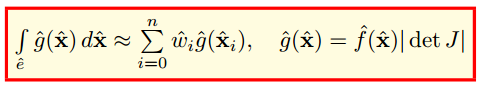
Voltage Sweep and Potential Profile
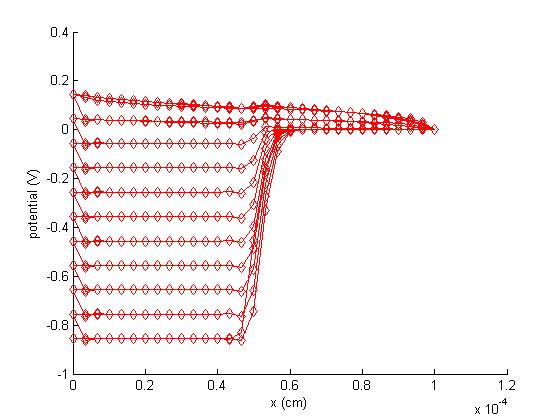
Current-Voltage Characteristics
stepsize = 0.01
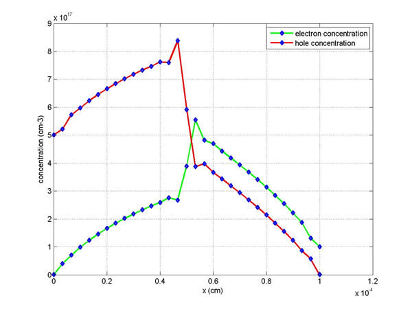
Electron/Holes Concentration
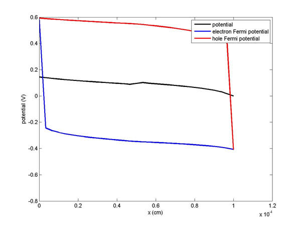
Fermi Potential
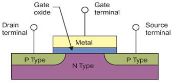
MOSFET
Device Structure
Current Concentration
Limitation
- Steady state analysis (no-transient)
-
Electrical Charactrizatino
Modules
Conductors - material propery (carrier concentraion, band-gap, fermi-level
Self-consistent ensemble Monte Carlo
Commertially available software Sentaurus Device [1]
[1] http://www.synopsys.com/Tools/TCAD/DeviceSimulation/Pages/default.aspx
[2] http://nanohub.org/resources/1565/download/ddmodel_solution_details_word.pdf
[3] http://www.mathematik.uni-dortmund.de/~kuzmin/cfdintro/lecture7.pdf
Device Modeling and Simulation of sub-micron press-fit MOS Transistor
Introduction
Parts - Conductor (Au?,Al), Insulator (SiO2), Semiconductor (Si, n-Si, p-Si)
Back-End Simulation of Bricks Fabrication
Simulating physical stress, oxidation and dopant diffusion.
Oxidation and Boron Diffussion
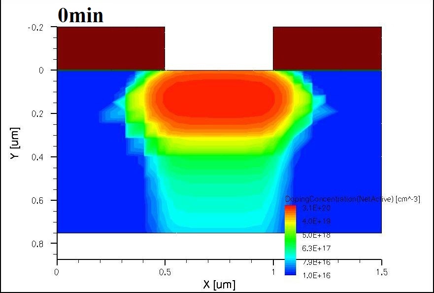
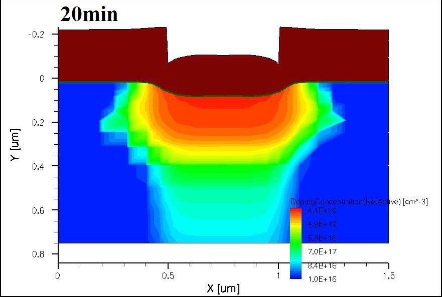
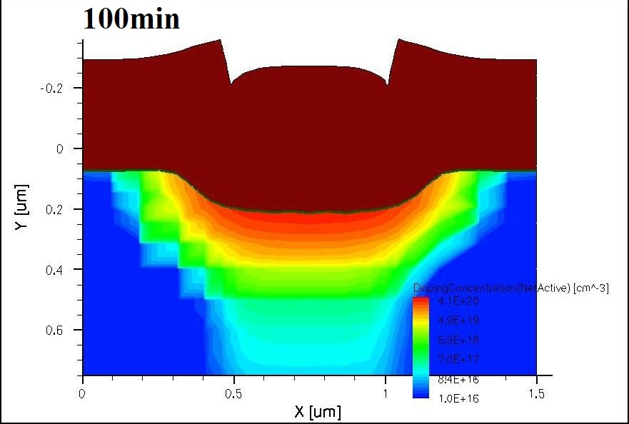
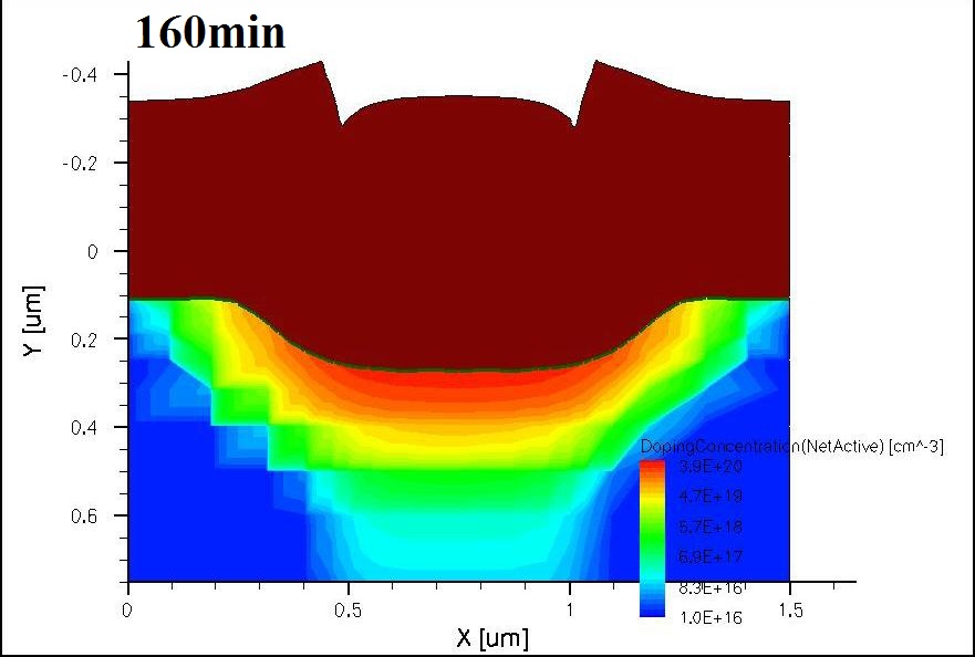
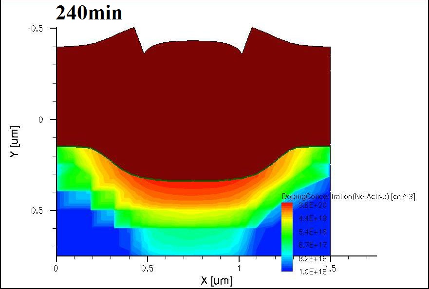
Next, stress vs Boron diffusion
Electrical Properties
Deriving electrical properties: Carrier concentration, mobility, conductivity.
IV/CV measurement of press-fit metal-semiconductor junction, p-n junction and MOS capacitor.
(Note: Fabricatin - Deposition and lift-off, Doping - Ion Implant and Annealing)
Ref
1 - vasileska.faculty.asu.edu
2 - http://www.ddm.org/DD07/Micheletti_Quarteroni_Sacco.pdf
Project (Old Idea)