This week focused on circuit board fabrication. In-System Programmers (ISP) are devices used to program microprocessor chips. Typically you would use a commercial ISP such as the Amtel AVRISP mkll. However This week's assignment was to fabricate an ISP of our own. Ali (a previous How to Make student) has written a very informative tutorial on how our FAB ISP actually works.
The process we used to fabricate a circuit board was as follows:
I've had some experience fabricating circuit boards over the last few months however I still ran into few issues which I've described below.
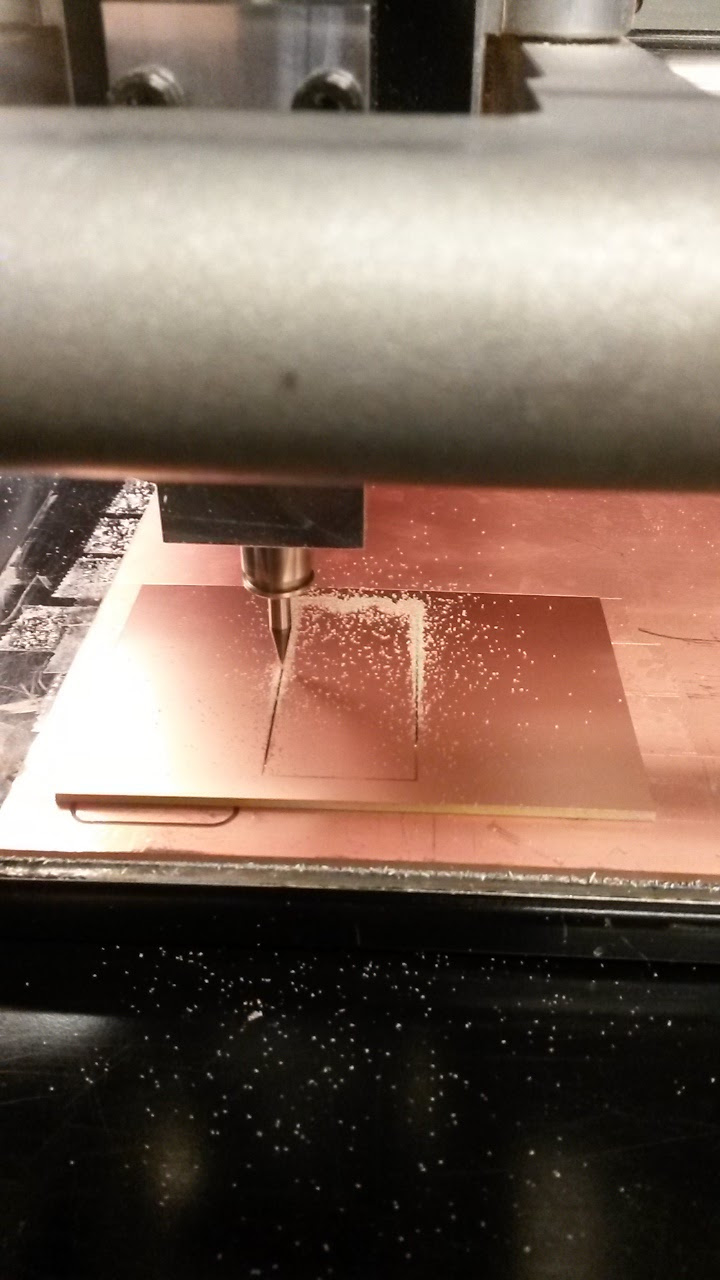
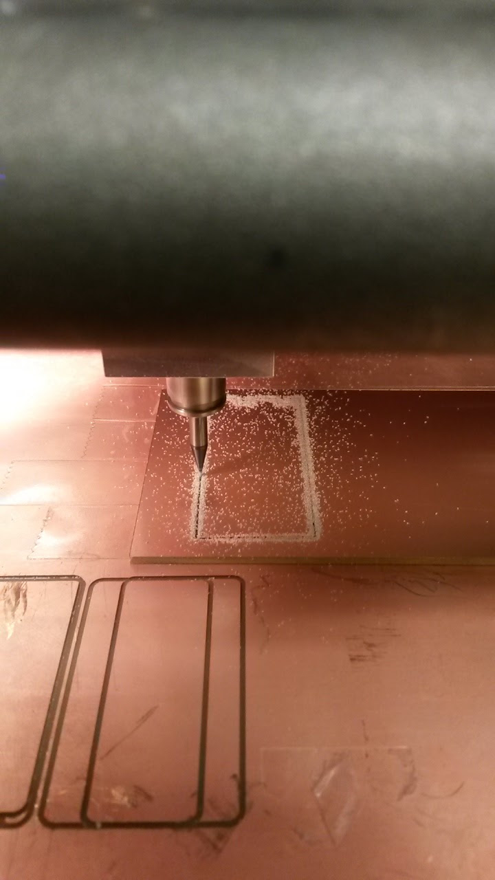
In these pictures you can see that the end mill hasn't cut at an even depth across the design. I recognised this just after I started the job when I saw that chips were not being formed consistently across the boards surface. This unevenness happened during two of my attempts, indicating that the sacrifical base layer was not even. To overcome this I moved my job into the center of the base plate.
Pretty clear what the mistake was here. For future cuts I made sure to check dimensions of your design in the 'read png' module of the mods software. I then did a rough measurement in x and y from the origin of the toolpath to ensure there was enough room.
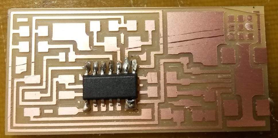
The traces of some of the components were incredibly thin and therefore required a bit of practice. During my first attempt at soldering the ATTiny I applied too much solder and didn't reflow it, resulting in bulky, non-shiny globs. In the process of trying to fix these connections, I applied too much heat to the chip, causing the shell to melt slightly.
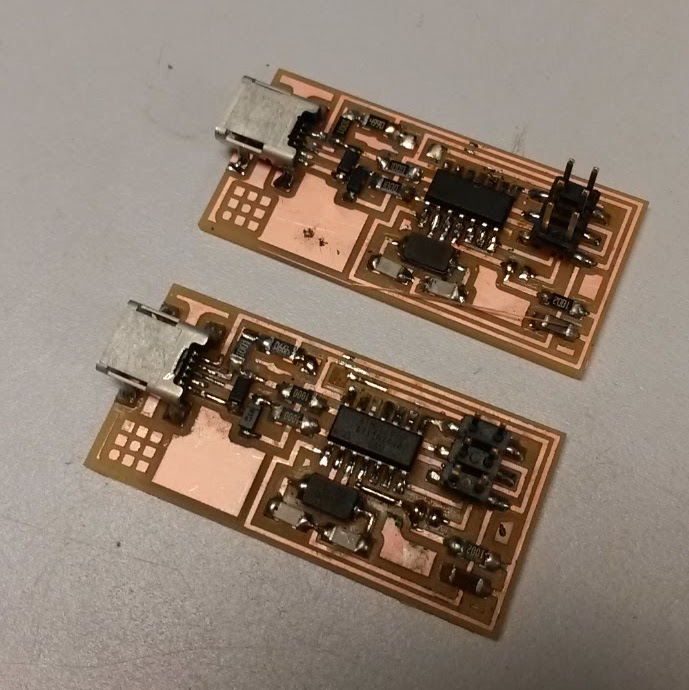
The rest of the stuffing went fairly smoothly. I had a problems programming the chip whereby I could successfully program it using the AVR ISP, however, after removing the jumpers, the board was not recognised as a USB device. After trouble shooting for a while I stuffed a second board was able to successfully program and detcet it.
Eric kindly debugged the first one and found that one of the Zener diodes had blown. So now I have two programmers, thanks Eric.
After programming our ISP's (for Neil's design), we had to remove two jumpers to then use it as a programmer. One zero ohm resistor pulls down the reset line to allow the chip to be programmed. The other one routes the power to a different location based on whether it's being programmed or programming.
The smaller Atmel processors like the ATTiny that we're using implement USB as a software protocol, this means you need to include an external time source. Initially, FabISP use an external timing source such as a crystal or resonator. The question is then how far off the USB timing can the external source be. The original 12MHz crystal used in the FabISP worked well, divided neatly down to 1.5MHz. When the design moved to a 20MHz crystal it didn't divide as accuratly down to 1.5MHz (frequency of low speed USB) but it worked just about OK. Using the resonator leads to very inaccurate timing. Extra note - the FabTinyStar uses the incoming bits to figure out how to tell time so adaptably tells time based on what it's hearing. Seems to be the best solution of all. In summary, favour the use of a crystal over a resonator, but also maybe try and implement FabTinyStar method of timing.
The VCC pin isn't a power source for the board, the VCC pin provides a reference to the programmer to tell it which voltage it is running at. Therefore, our boards require an external power source to be programmed which we provide via a USB. This is why you need to have the board you're trying to program plugged into the USB port of your computer at the same time as having the programmer plugged in to do the programming.
The chips have different types of memory:
USB power is 5V. Transmitted signal levels are 0.0–0.3 V for logical low, and 2.8–3.6 V for logical high level. A Zener diode is used to clip the 5V down to 3.3V to supply the data lines. This is combined with a resistor to limit the current through the diode.