week 4: electronics design
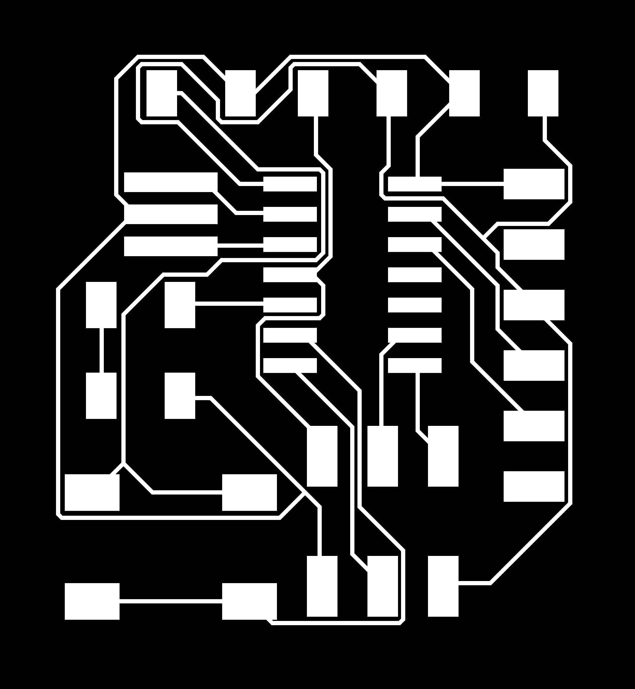
This week, the assignment was to redraw the echo hello-world board, add a button and LED to the board, check the design rules, and finally make and test the board. We were given this design of the original echo hello-world board:
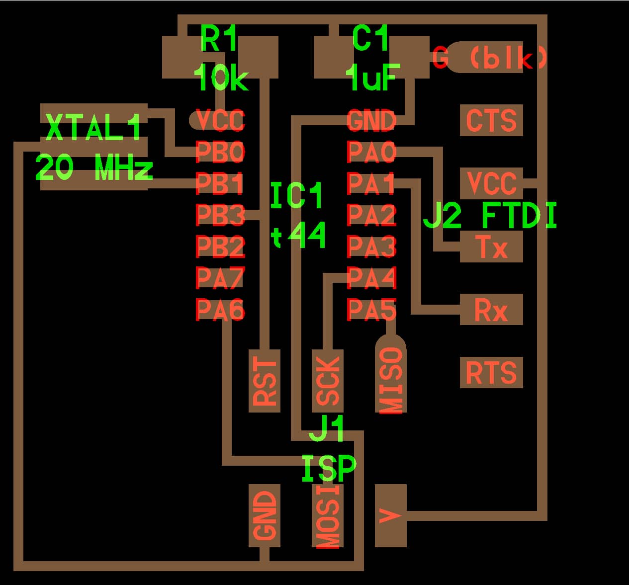
The original echo hello-world board.
I have no previous experience with electronics design or any of the software mentioned in class, so I used Eagle to design my board for this week. I attempted to jump straight into using Eagle, and ran into some problems right away. I wanted to import the fab library into Eagle, but I couldn't find the Download File option in Chrome, so I copy and pasted the text of fab.lbr into a text editor and saved the file. I was able to import the library and all the components were listed, but when I tried to add a component, I would see an error about it expecting text at a certain line in the file. I switched to Safari, found the Download Linked File option, and when I imported this directly downloaded version of the library into Eagle, I was able to add components.
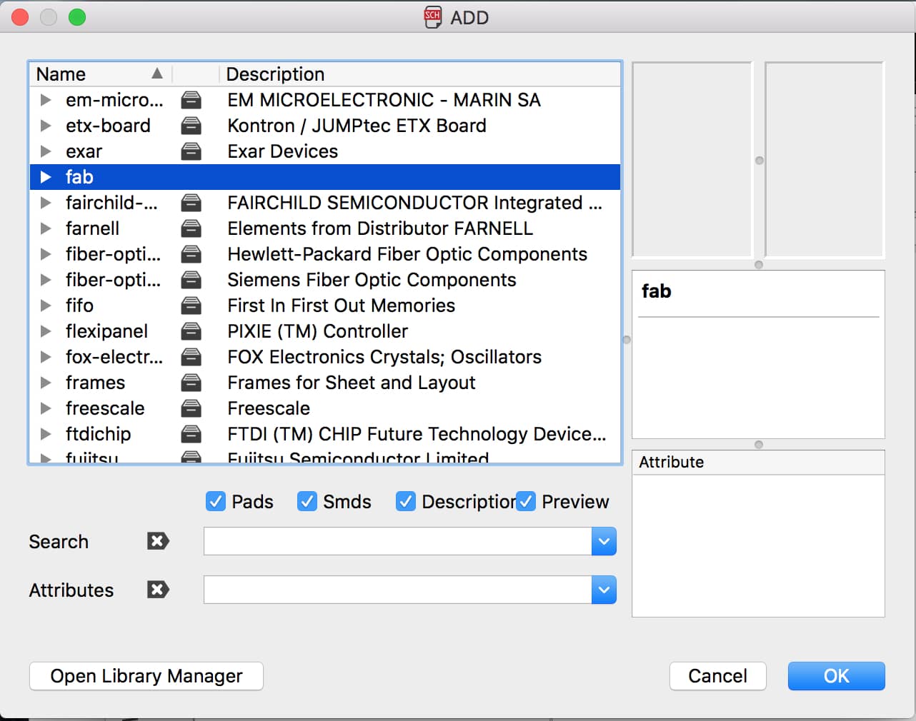
I successfully imported the fab library into Eagle.
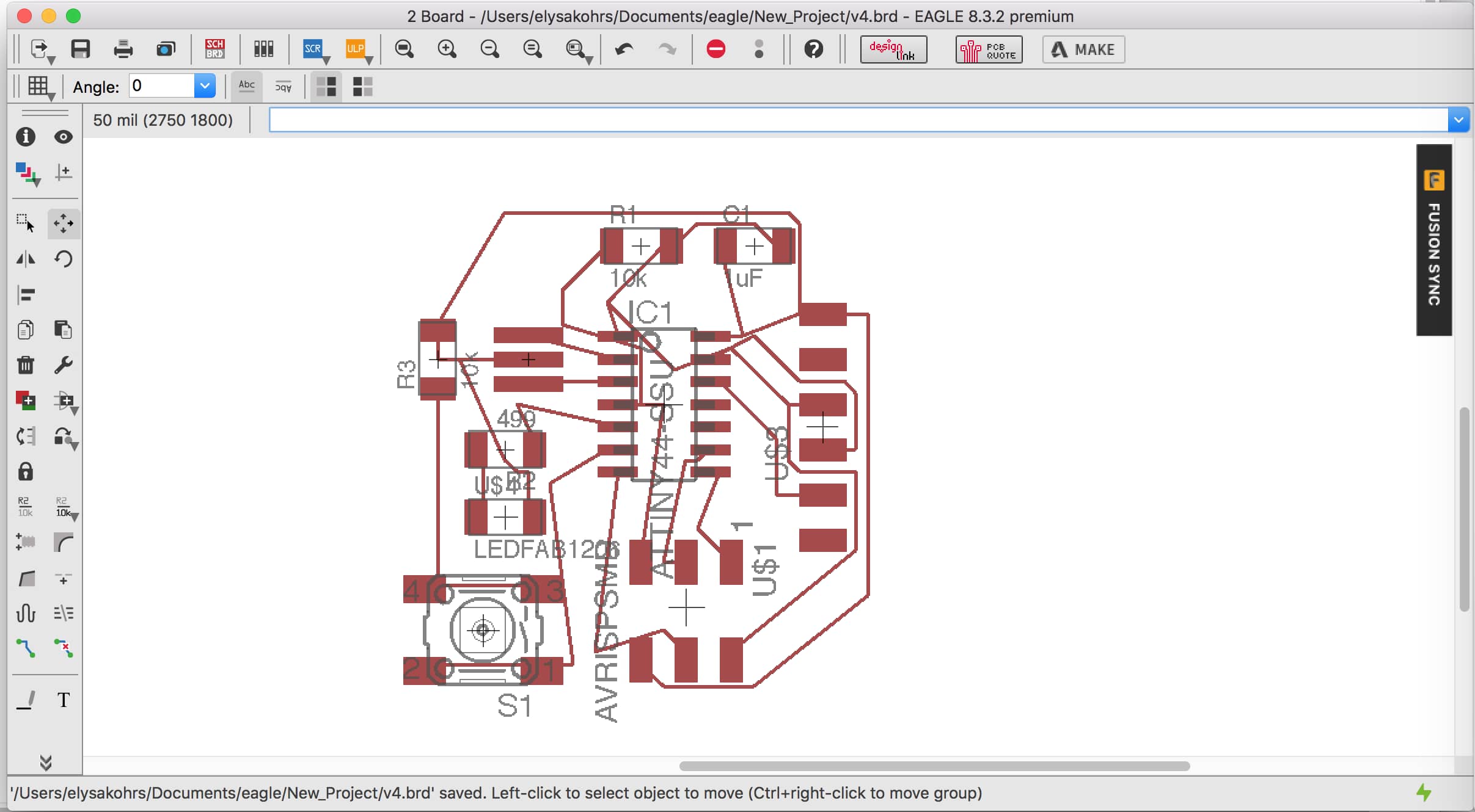
I started trying to find the components of the echo hello-world board and add them to my schematic. I quickly realized that I knew how to type the add command, but didn't know much aside from that and overall had no clue about how to use Eagle. I put my schematic design on hold and watched a series of about six short video tutorials online and felt much more knowledgable about Eagle and the process of going from a set of components to a laid out board. I returned to Eagle and finished adding components. Then I proceeded to use the net tool to connect everything how it is in the original board. Next, I added the LED and button components, plus resistors, and connected them to PB2 and PA7.
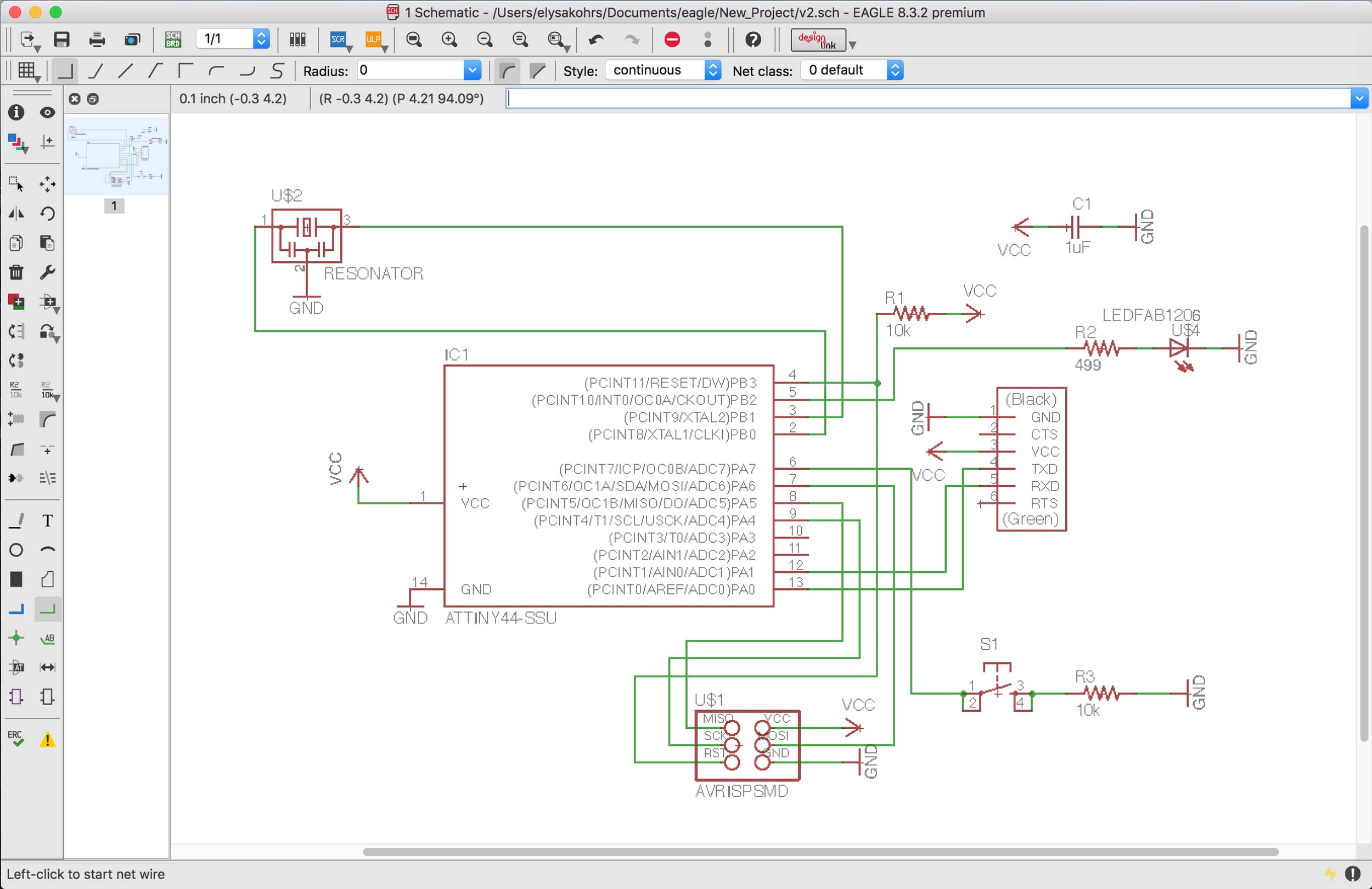
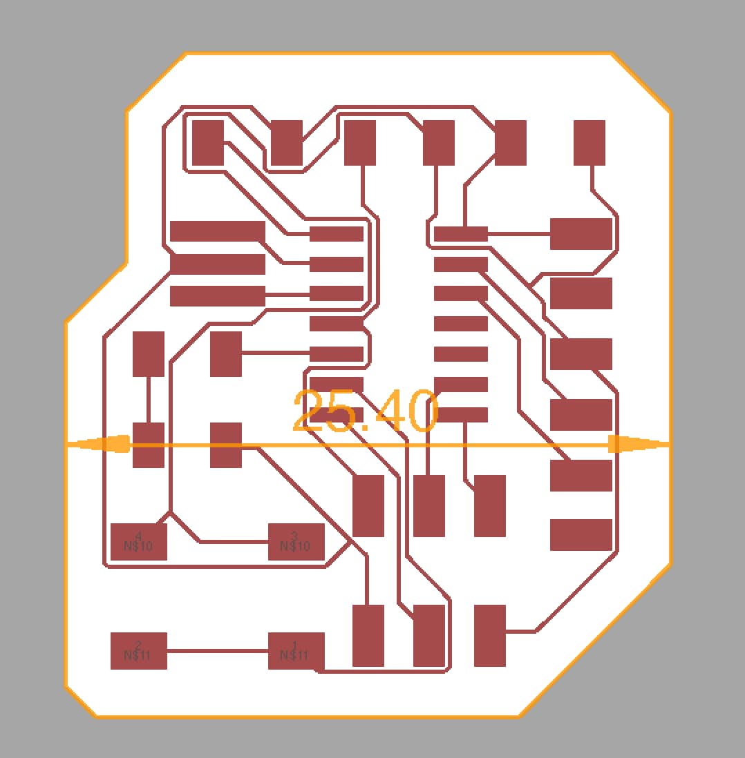
The finished schematic in Eagle.
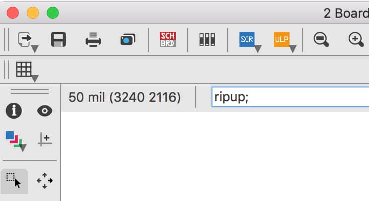
I switched from schematic view to board view in Eagle and started moving around components, trying to settle on a layout that was space-efficient and would minimize having too many complex routes. I reached a point where I was pretty satisfied and felt ready to route. I decided to try the autorouting tool, and it gave me multiple options that required no vias, so I chose one of them. I wanted to make my board close to as compact as I could though, so I moved some of the components closer together in areas where it seemed like there was room. The problem was that when I did this, the routes got changed and ended up following odd angles. I did some googling and discovered an amazing command, "ripup". This command removes all the routes, so after I adjusted the components, I used ripup, and then redid the autorouting with the components in their new locations. I went through this process a couple of times, trying to find a configuration that was compact but didn't require vias.
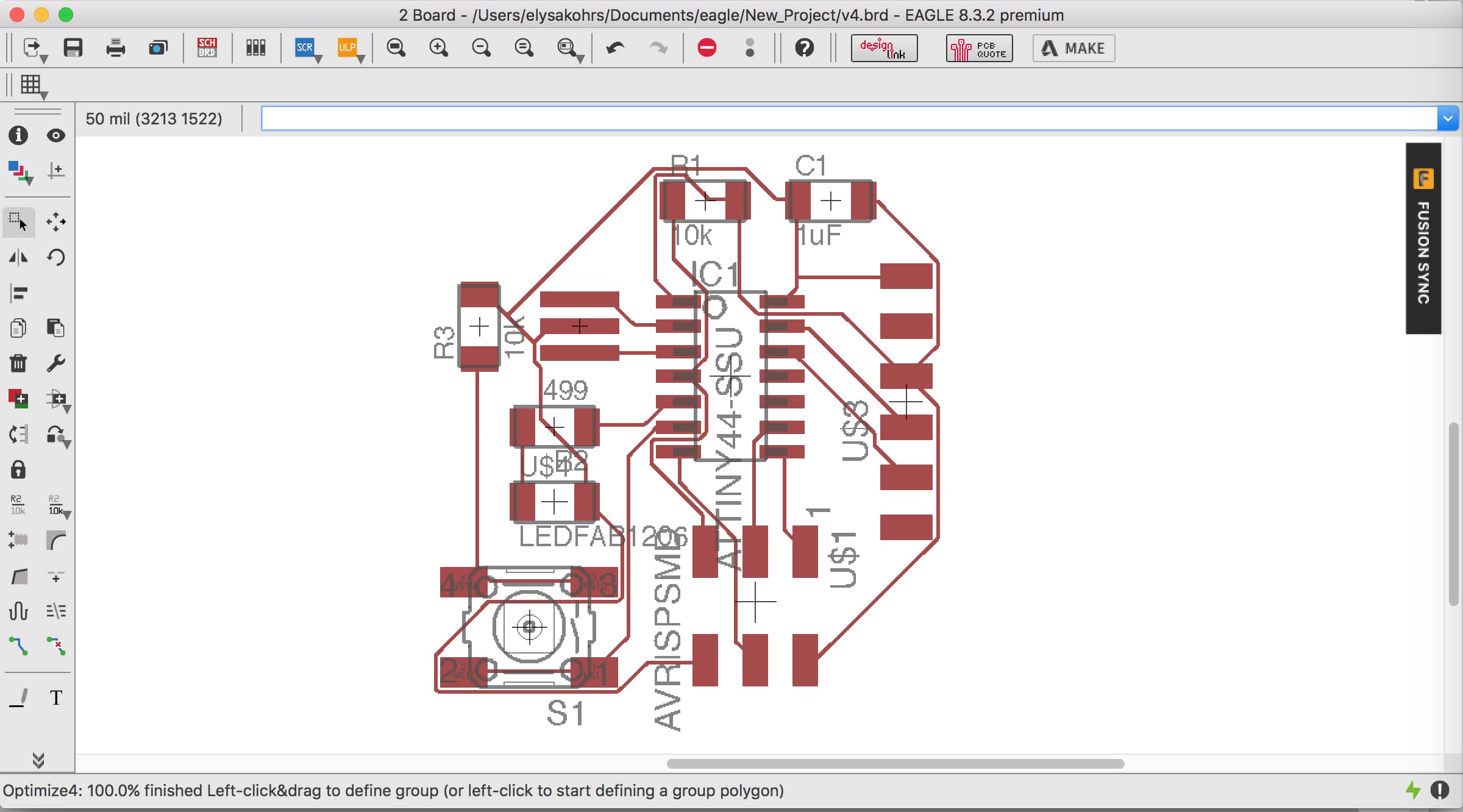
An early design of my board.
Weird angled routes arose when I moved components after routing.
The ripup command became my friend.
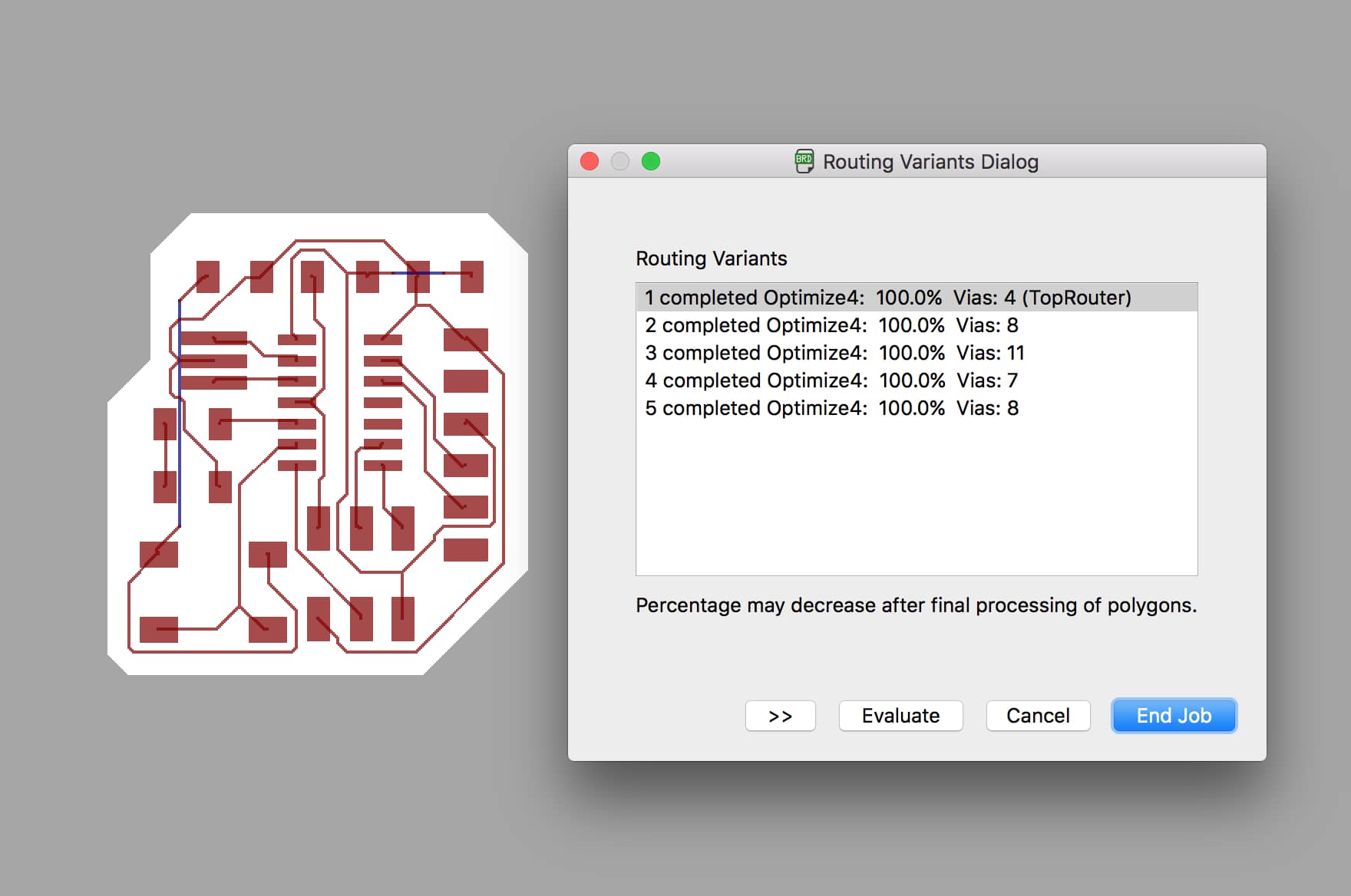
I used autorouting, but moved components around when all the routing variants required vias.
Once I laid out the components and routes, I wanted to change the outline of the board to be a non-rectangular shape. I used the wire tool and created these dimensions for the board. Then I was ready to export the traces and the outline so that I could build the board. I figured out how to export only the top layer, and then only the dimension layer as PNG files. At this point, I happened to be looking at this week's page on the HTMAA website, and saw that one part of our assignment was to check the design rules of our board. I went back to Eagle and used the Design Rule Check button, and found out that were 25 errors with my board. They were all due to the dimension wires for the board outline being too close to the components and traces. I moved the dimensions further out which got rid of the errors. Then I re-exported the traces an outline as PNG files. I figured I was prepared to mill my board the next day.
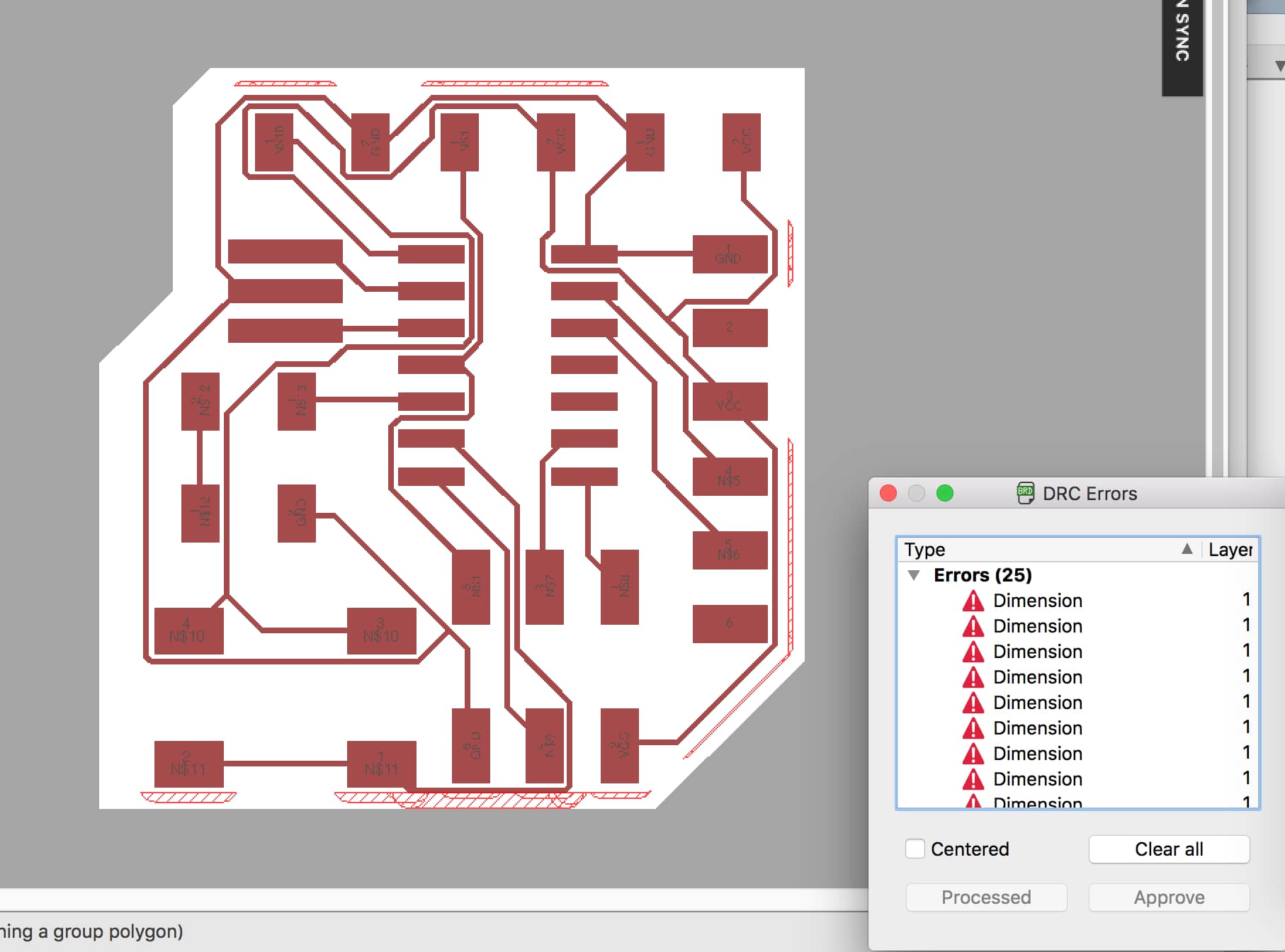
Lots of errors when I checked the design rules.
The PNGs of the traces and outline that I exported from Eagle.
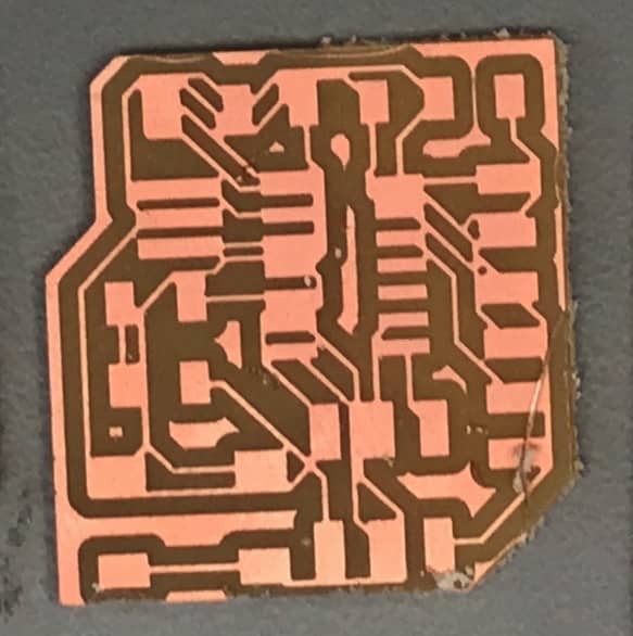
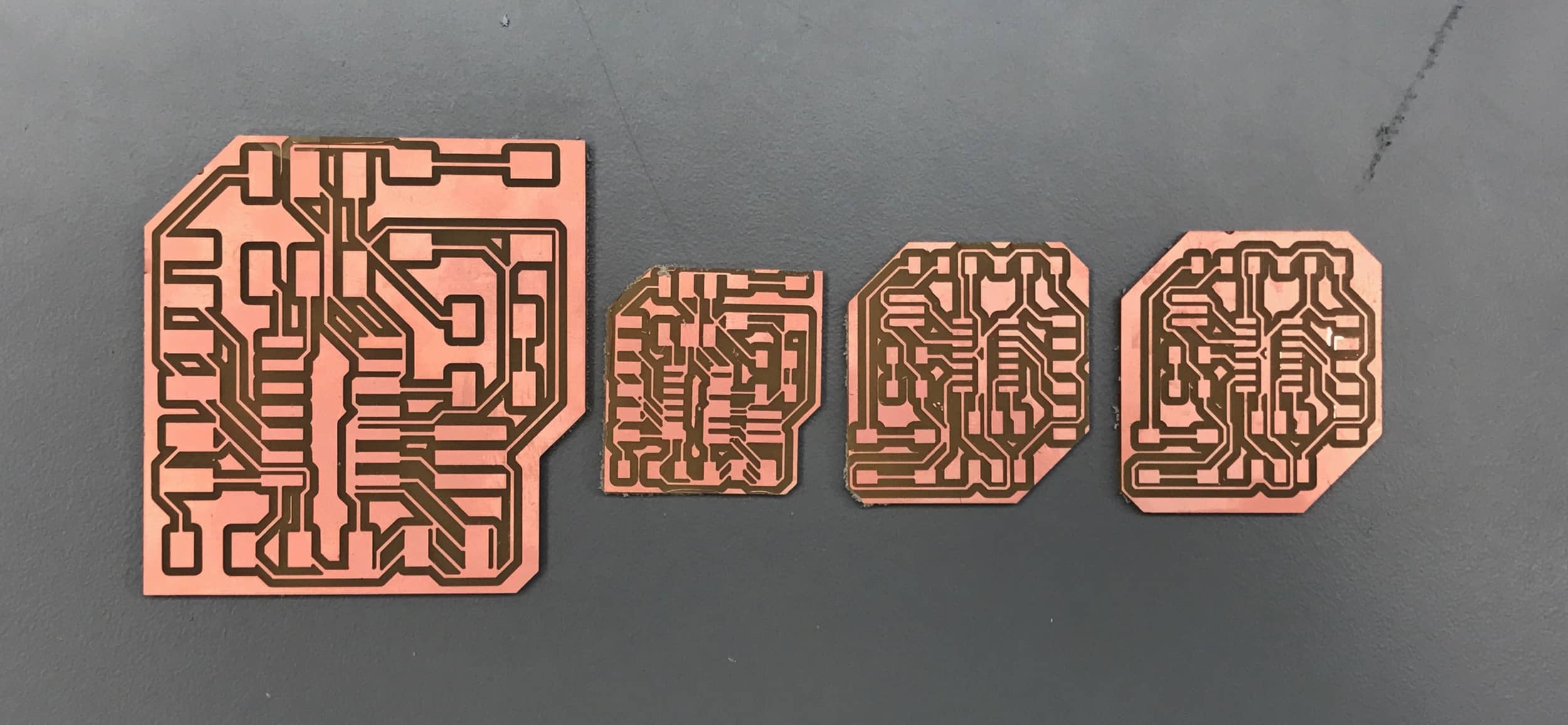
Milling a board ended up being a major struggle. At first, there was an access error so the mods server couldn't communicate with the milling machine. Gavin helped me, and that resolved pretty quickly. I was able to send the traces and the outline to the machine using the two PNG files I had exported from Eagle. It worked with no problems, although it was difficult to remove the cutout PCB because it was on a section with double-sided tape. Once I removed the board, I went to gather all the components so I could begin stuffing the board. After a lot of looking and asking people where things were, I had all the components and was ready to solder. But then I placed the ATTiny44 on my PCB and realized that something was very wrong. The board was way too big for the actual components.
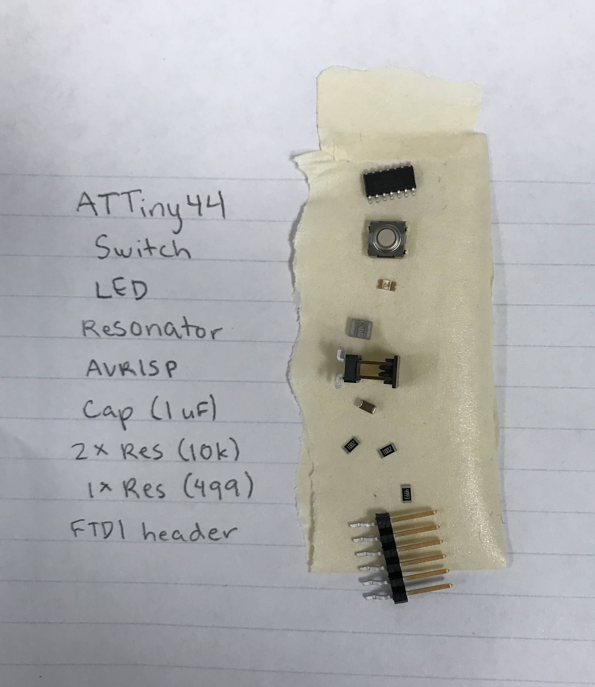
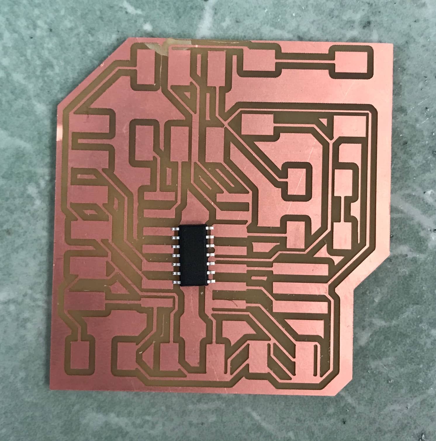
I gathered all the components and then realized I had a problem.
I'm still unsure of why this happened, but somehow, between exporting to Eagle and sending the file to the mill using Mods, the PNG file was registered by mods as being twice its actual size. I made sure the DPI entered in mods matched the DPI of the file I exported from Eagle, and then used the dimension tool in Eagle to figure out the size the board should be and deduce that its size in mods was double that. I solved the problem by doubling the DPI entered in mods to be 2x the DPI that I used to export from Eagle, but am still curious as to why the sizing is off.
Checking dimensions in Eagle to figure out whether mods was doubling the size.
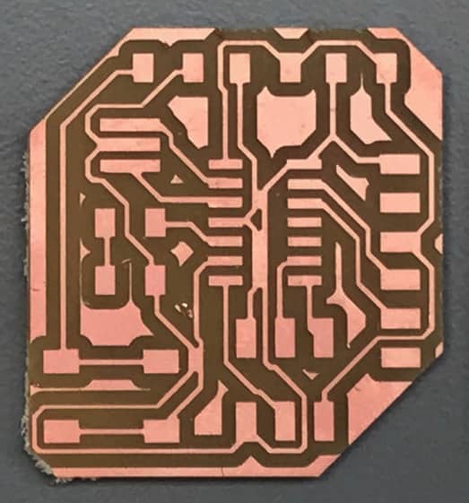
I remilled the same board but with the DPI doubled to account for the weird sizing. The milling process went smoothly, but when I removed the board, I noticed that a couple traces near the FTDI header were connected, when they should have been separate. Another student suggested that this was because the spacing between traces/components was too narrow. I went back to Eagle and adjusted the Clearance options of the Design Rules. I spread components apart further, redid the routing, re-exported the files, and milled the board again.
Attempt #2 had some routes connected that shouldn't have been connected.
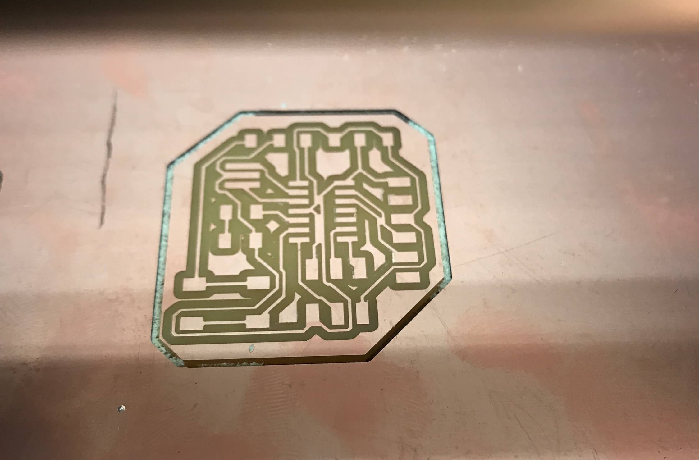
On my third attempt at milling the board, the outline became a problem. I had noticed that the outline was a bit close on the first two boards, so I made the dimension wires thinner in Eagle. Unfortunately, I made them too thin and the top and bottom edges were too close to the edges of the PNG, so only the left and right sides of the outline were cut when I sent the outline to the mill. I went back to the outline PNG file with the thicker dimension wires and immediately sent that to the machine. It cut all the sides of the outline, but was too close to the components/traces.
In attempt #3, the outline was too close the traces.
I could have dealt with this outline proximity problem by moving my dimension wires further away from the components and traces, but I didn't want significant empty space around the edges of my board, and according to the design rule check, the outline was far enough away. Instead, I exported the PNG files using the Window option instead of the Full option, so that the top and bottom edges of the outline wouldn't be too close to the top and bottom of the PNG. I milled these traces and outline, and finally had a board with no problems that I noticed.
Fourth time's the charm?
I still had all the components ready that I had gathered earlier, so I began soldering. My soldering has improved since the first PCB we made two weeks ago. Sometimes I still have trouble with getting peaks, but trying to use less solder has helped. I think it probably took me half as long to solder this board compared to my first PCB.
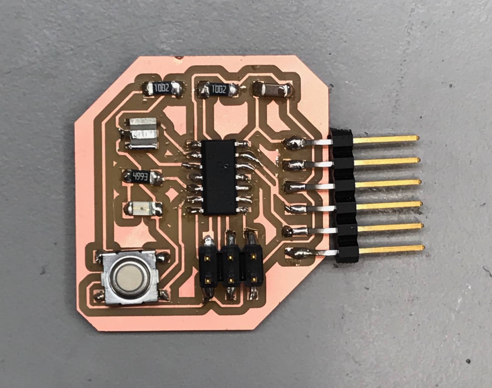
Post-soldering the components to the board.
I ran out of time to program and test my board, but this week I've become fairly comfortable with using Eagle, and I learned a lot about Eagle and milling in my three failed boards.
Learning from failures.