to start adding components.
I messed around with KiCad last night. For open source software, it works quite well (much better than FreeCad). I didn't know I needed to install the fab library so I was having trouble finding the components.
Download fab library and save into the default directory for component libraries: /Library/Application Support/kicad/library
Then
Make sure you also save the fab.pretty folder into /Library/Application Support/kicad/modules and add it as a footpath library to avoid errors later!
.lib file and .pretty folder have the same file name and nickname. Also, potentially you need to update fab.lib in order to make the transition from scheme to pcb go smoothly. (I've outlined these steps here)
to start adding components.To start off, I will reproduce the example board.

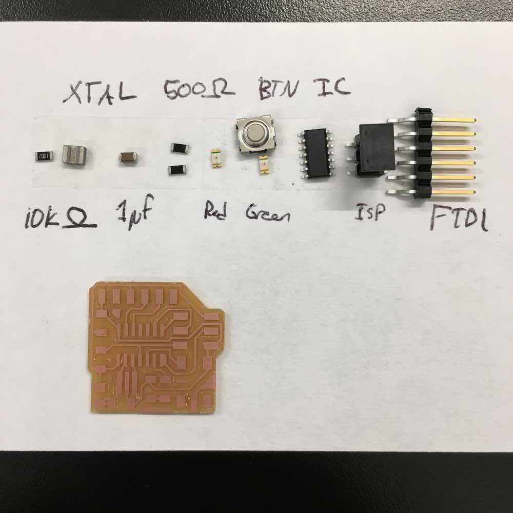
R1 is a RES-US1206FAB.
C1 is a CAP-US1206FAB.
XTAL1 is a RESONATOR.
IC1 is the ATTINY44-SSU.
J2 FTDI is a FTDI-SMD-HEADER.
J1 ISP is a AVRISPSMD.
After I placed all of these components, I renamed some of them to make everything more clear. You can rename components by double clicking on them.
I added another resister, LED and switch to add to the board later.
R2 is RES-US1206FAB.
M1 is LEDFAB1206.
S1 is 6MM_SWITCH6MM_SWITCH.
Adding wires is slightly wonky.
I found this helpful tutorial and decided to clean the schematic by labelling the wires before routing the PCB.
I got a bunch of errors saying the footprint wasn't found! I'm guessing I only imported the Fab schematics library and not the footprints for all the components as well.
I just checked Preferences > Manage Footprint Libraries… and my suspicion was confirmed. I had to go back to gitlab and download the entire fab.pretty folder into /Library/Application Support/kicad/modules.
I did this and it didn't work it first! I looked into the folder that I had added and realized that after I had downloaded and unzipped it, the folder with the models was in a subfolder. Fixed the path!
But…. I'm still getting the same error. I renamed both files to make sure they had the same name, and ended up ruining my schematic in the process.
It seems like KiCad recognizes the footprint library but cannot see the kicad_model 🧐
So I think I figured out what is going on. Footprint files need to be name spaced, with the nickname of the library.
8/7: Looks like this bug has been reproduced! Lincoln is also using KiCad and ran into this issue as well. Glad that I wrote down the steps to fix it.
Once I managed to get the footpaths working, the routing itself was quite pleasant. KiCad will show you what needs to be connected (based on your scheme — so make sure this is right before routing otherwise you'll need to go back and redo stuff).
Yes, this is a Chekov's Gun moment
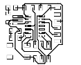
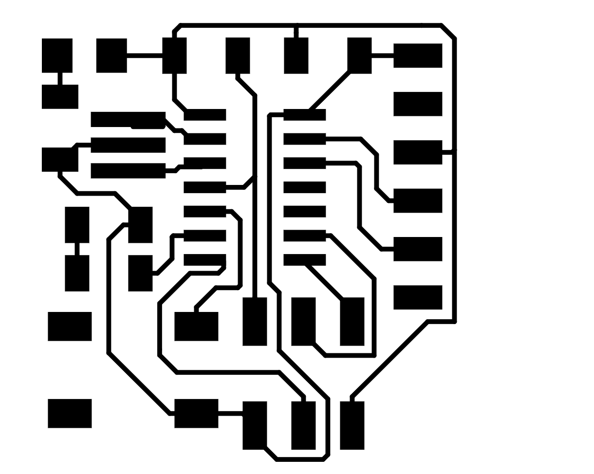
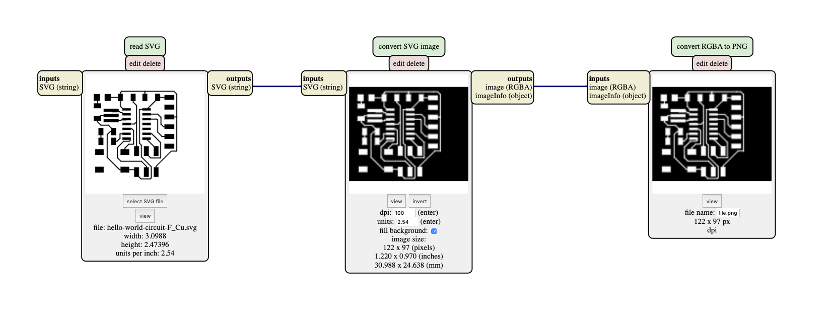
When I finished routing the board, I exported both the traces and the outline as svg files
File > Export > SVG...
Traces: Select the 'F.Cu' layer with the 'Black and White' print mode
Edge: Select the 'F.Cu' layer and then whatever technical layer you outlined the edges on.
I used "Edge.Cuts" which I think is right because once I had drawn the outline, I wasn't able to create traces that extended over the edges I had defined.
When I uploaded to mods to check the tool traces, I realized that I
0.127mm * 3 between routes and anything else should allow the milling machine to cut without overlapping different components.
https://forum.kicad.info/t/updating-pcb-after-changes-made-to-schematics/587/9
"Edit > Clean Up Tracks and Vias…" is really important if you make changes to the schema file.
Check with only one offset in mods to see tool path
Use polygon tool to create edge.
Unlike milling the programmer board in the week on electronic production, this time the file I am giving to the SRM-20 is a svg — because KiCad doesn't export PNGs.
I need to figure out how to run the svg version of mods on the computer that connects to the SRM-20.
Rob actually recommended converting the svg files to png instead of trying to get mods to work. So I will do that. Should be reasonably easy thanks to imagemagick.
Turns out this isn't as easy as one might think. There are a number of approaches on StackOverflow.
convert hello-world-circuit-F_Cu.svg traces.png. I think I need to specify the resolution, which is where this gets tricky. Hmmm. Before I overly commit to the ImageMagick route, let's see if there are any alternative approaches.
qlmanage -t -s 1000 -o . hello-world-circuit-F_Cu.svgThis will only work on OSX, but it gave me a decent image.
mogrify +antialias -density 2000 -verbose -format png *.svgThis didn't really work at all.
qlmanage outputs an adequate png of the board, but I still have to specify the sizing which is not ideal.
I looked at the raw SVG to see if the size was hardcoded and found this:
<svg xmlns="http://www.w3.org/2000/svg" version="1.1"
    width="3.0988cm" height="2.47396cm" viewBox="0 0 12200 9740 ">
I think if I just use the units from the view box that might work. Going back to using imagemagick because I can specify both dimensions.
convert -size 12200x9740 hello-world-circuit-F_Cu.svg traces.png
Really thought that might work, but it didn't.
What's especially frustrating is that I know mods is able to process SVG files. The issues is just that the version running on the desktop linked with the printer, can't. Maybe I can design my own mods workflow to do it for me?
I now have a simple workflow to go from an SVG to a PNG! Maybe at some point, I'll try to recreate the entire flow.
I realized probably the easiest thing would be to download the SVG SRM-20 program locally on the desktop computer. This allowed it to connect. No need to convert to png after all!

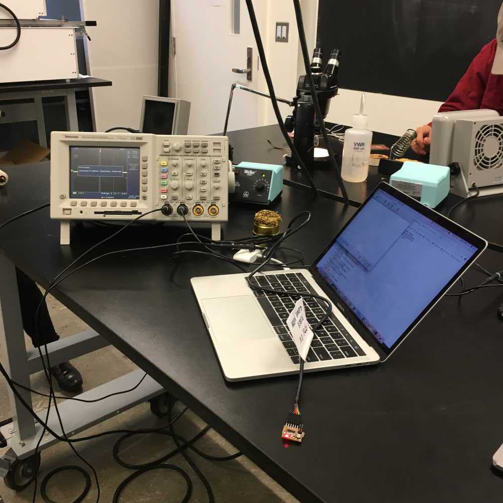
I'm going to take a look at my documentation on Electronics Production.
The key take aways are:
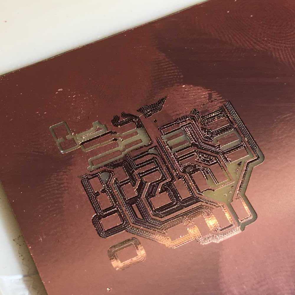
I found a copper blank, washed it, found the tape and put it on. When I placed it on the sacrificial layer I made sure it was well connected.
I need to make sure the bit is the correct size for the traces ( of an inch) and position it properly relative to the board.
My origin is x:110, y:100, z:6
Before I mill, I'm making sure that the defaults in my new local version of mods match up with the original.
I started the job and for some reason it started milling in the wrong area. It seems like the origin is anchored at the bottom left of the file.
I updated the origin to x:110, y:75, z:6 offsetting the y point by 25mm. I arrived at this value by looking at the height of the svg file, according to mods.
I am a little worried right now because, I'm watching the milling process right now and I think that parts aren't being milled because the bit isn't going deep enough.
Yeah, it didn't work and I'm not sure why. I'm going to try rerunning the job but increasing the cut depth slightly from 0.004 in to 0.00425in. 🤞
Worked a little better this time but still missing parts of the board. Why is the board so uneven?
I'm trying a third time and increasing the cut depth to 0.005in, which is already looking better… but still not deep enough apparently. I terminated the job early and repositioned the drill.
The last attempt nearly fixed it. Trying 0.0055 now. While that job is running I'm going to look up how to edit SVGs. It would have beenn really nice if I could just mill the parts that that didn't work the first time. (This could even be made into a mods component).
x: 110, 48, 6
x:140, y:48, x:6
x:115,y:75, z:6
I finally managed to mill the traces.
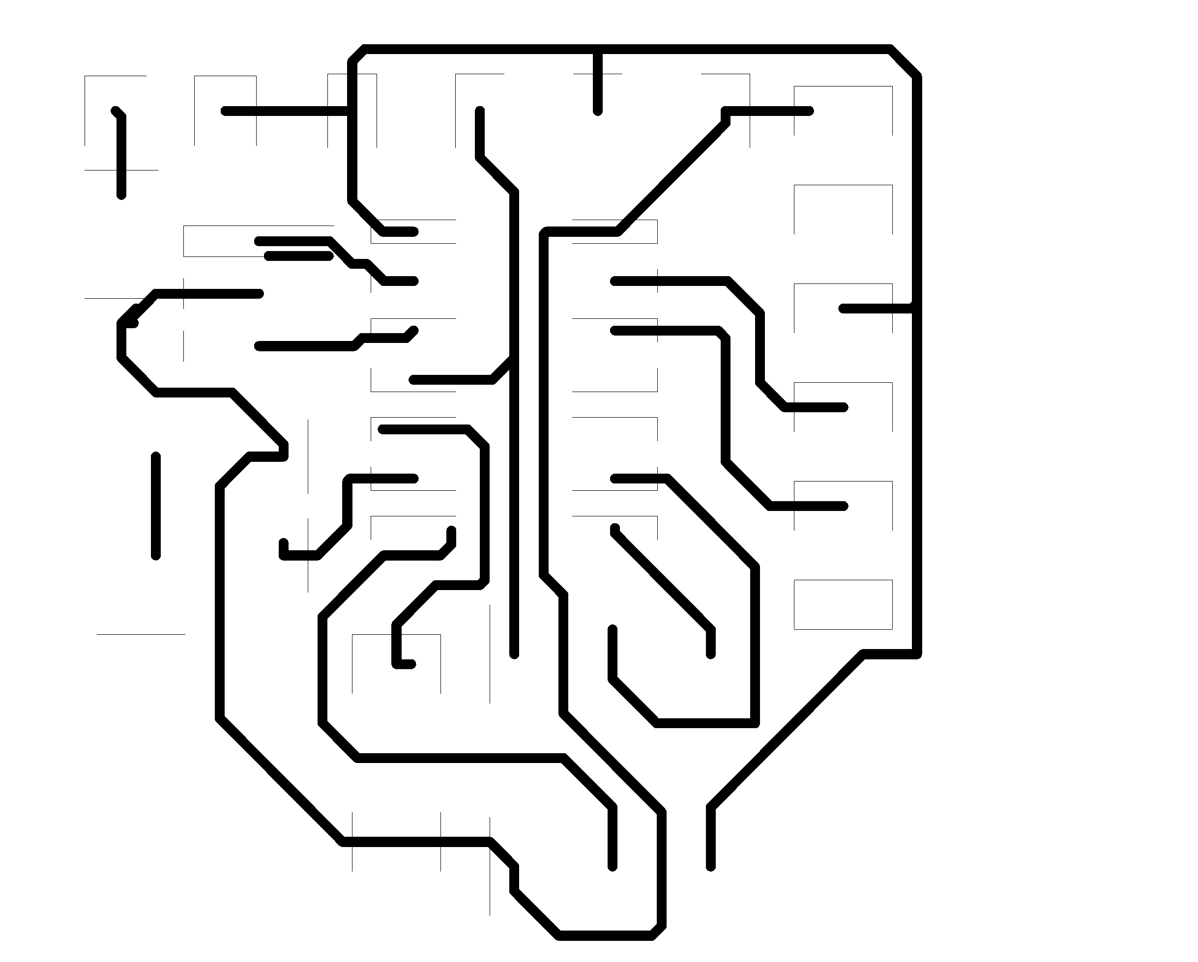
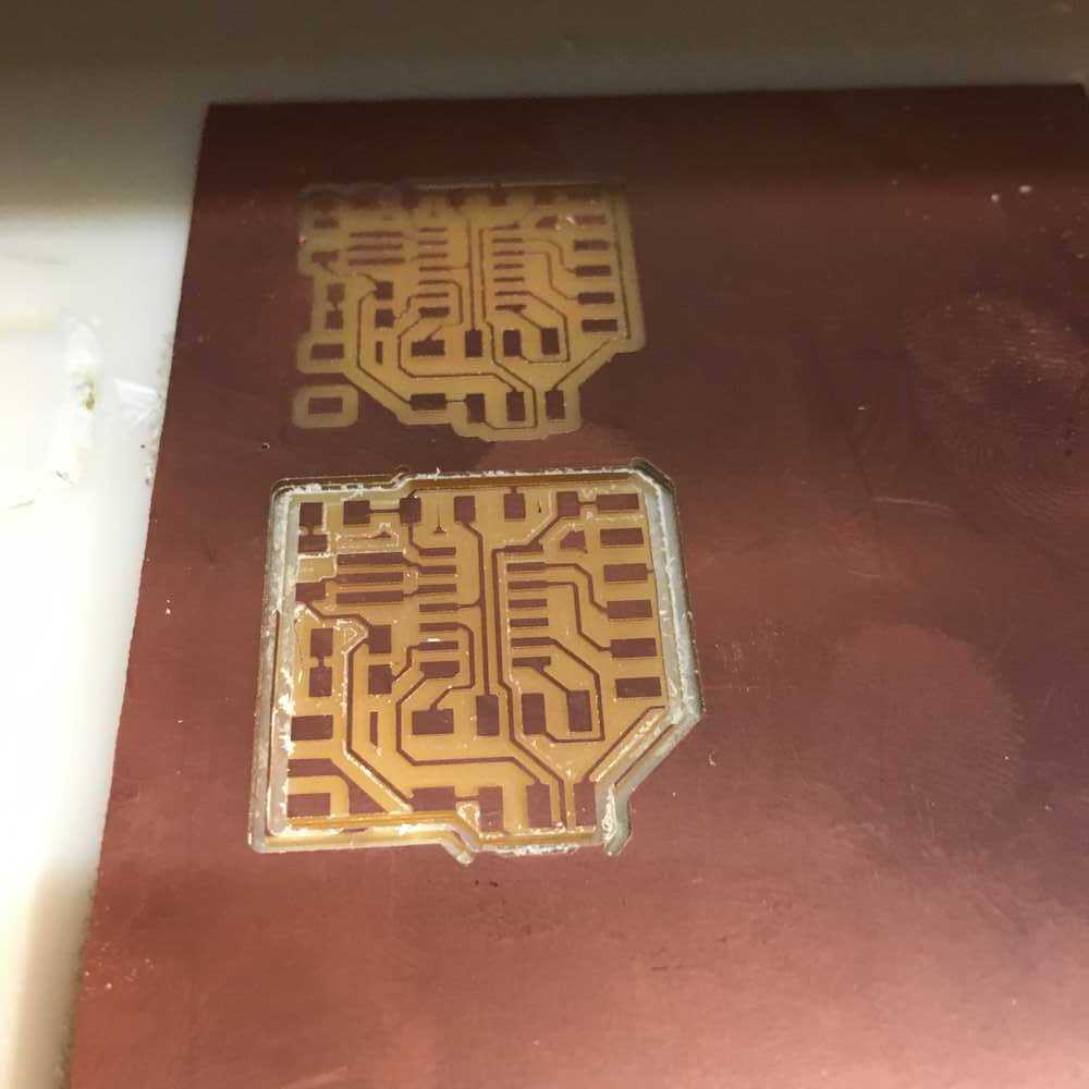
Milling the outline proved to be the biggest challenge. As I used KiCad to prototype my board, I could only export SVGs. This was slightly annoying for the traces but proved to be a huge issue for the outline.
I needed to manually convert the exported SVG file from a bunch of paths to a single closed polygon. This can probably be automated or even just circumvented by using a different tool in KiCad to make the outline.
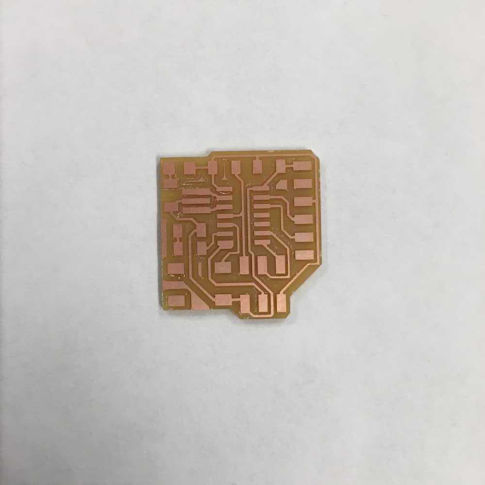
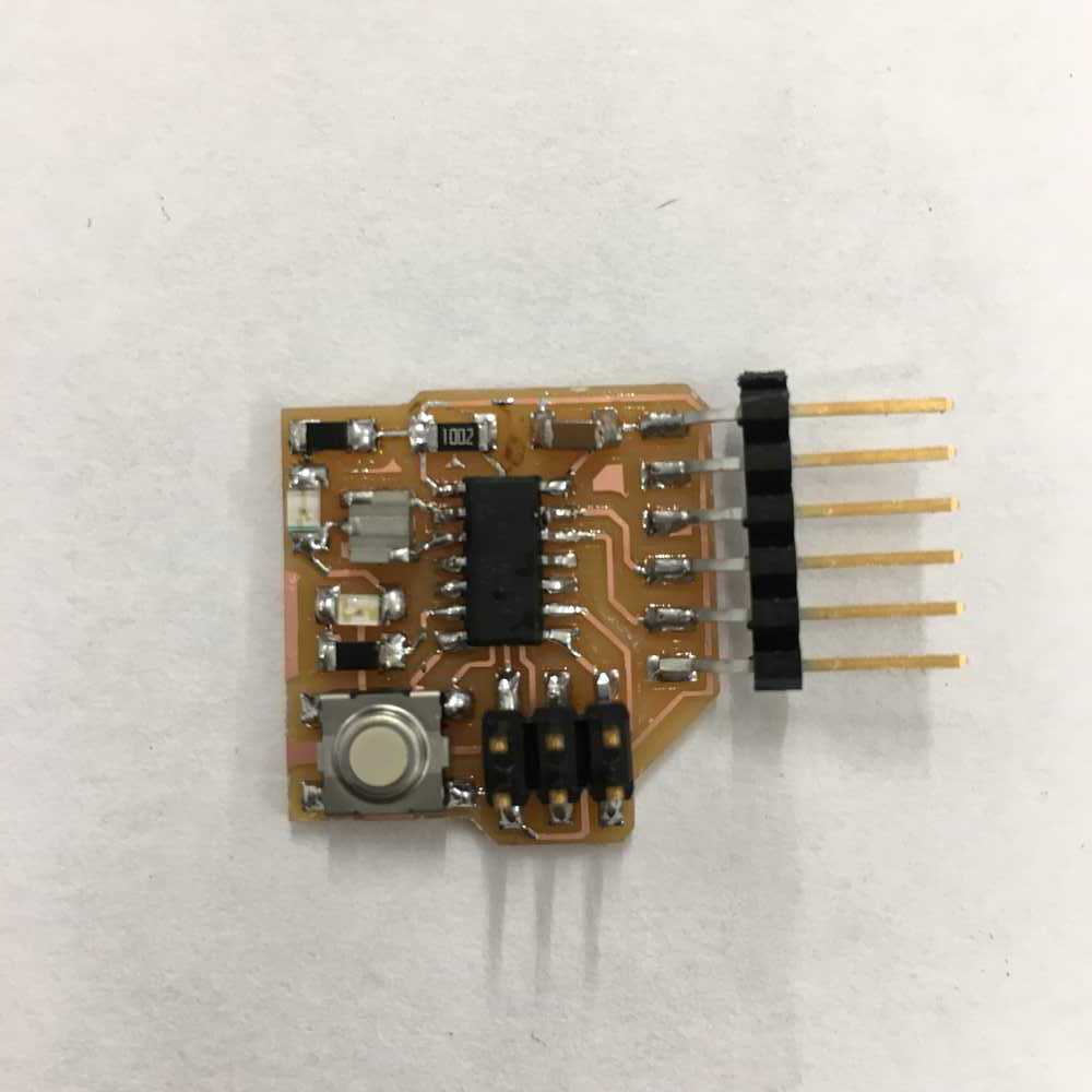
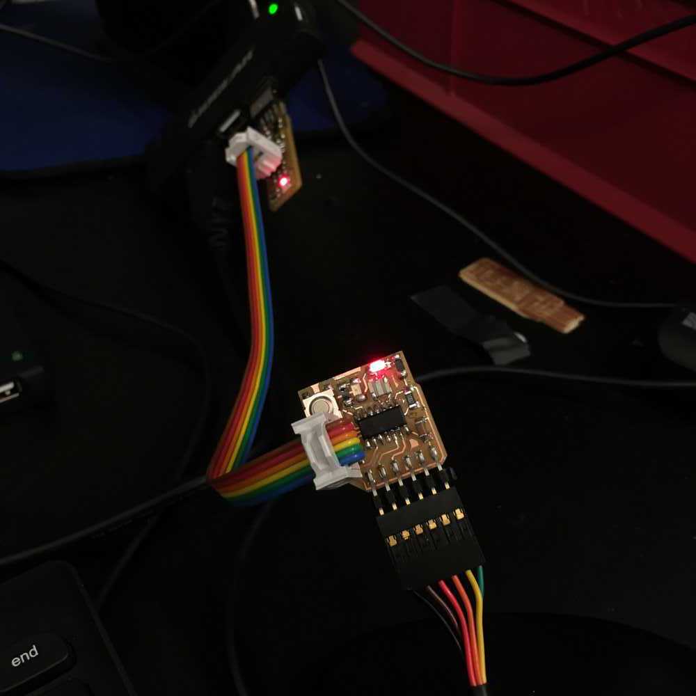
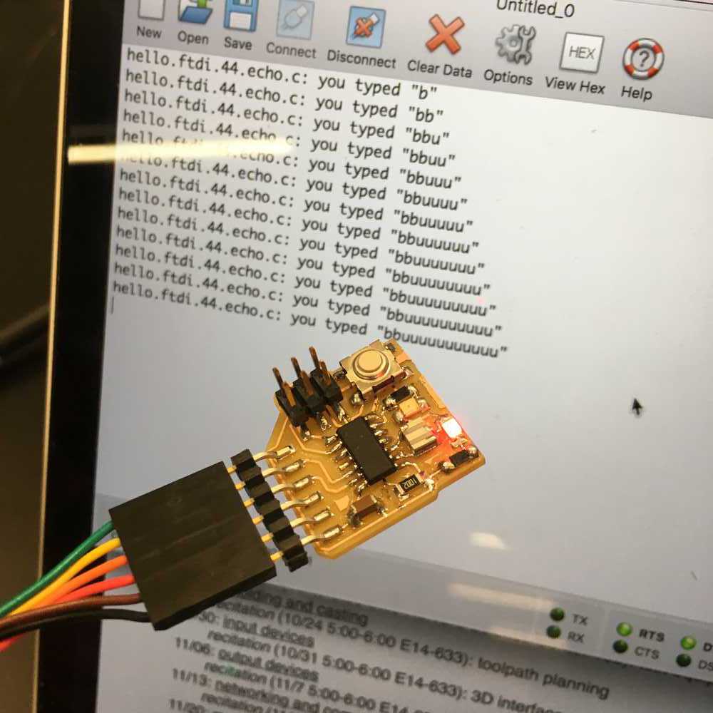
Nothing too notable. I took the lessons I learned from soldering the programmer board and everything went pretty smoothly.
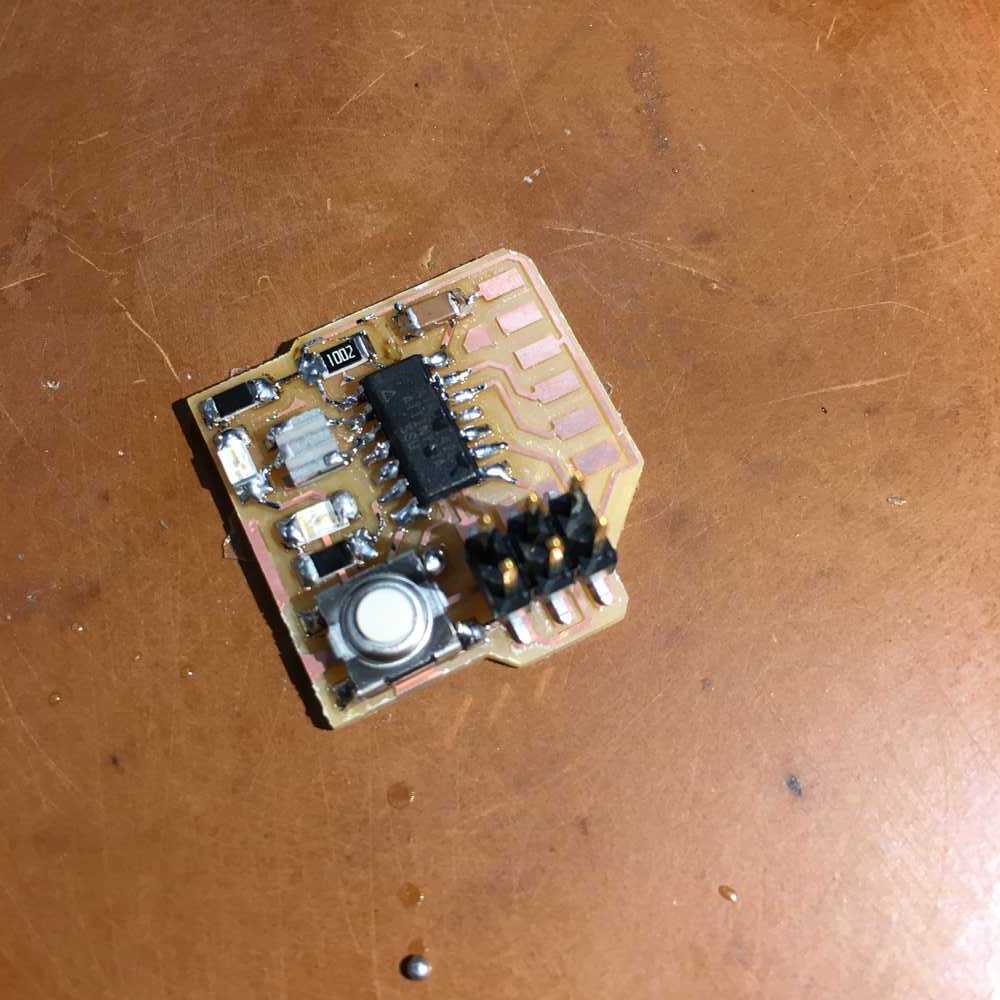
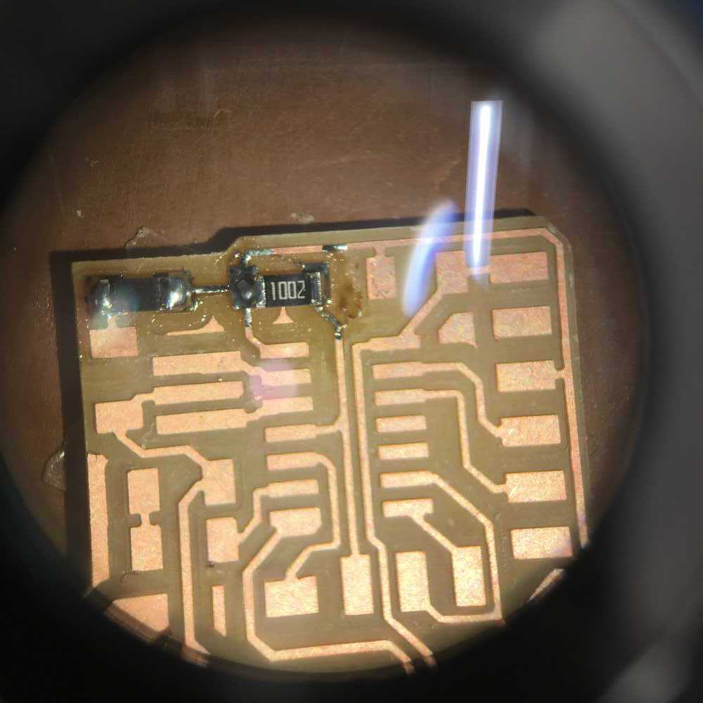
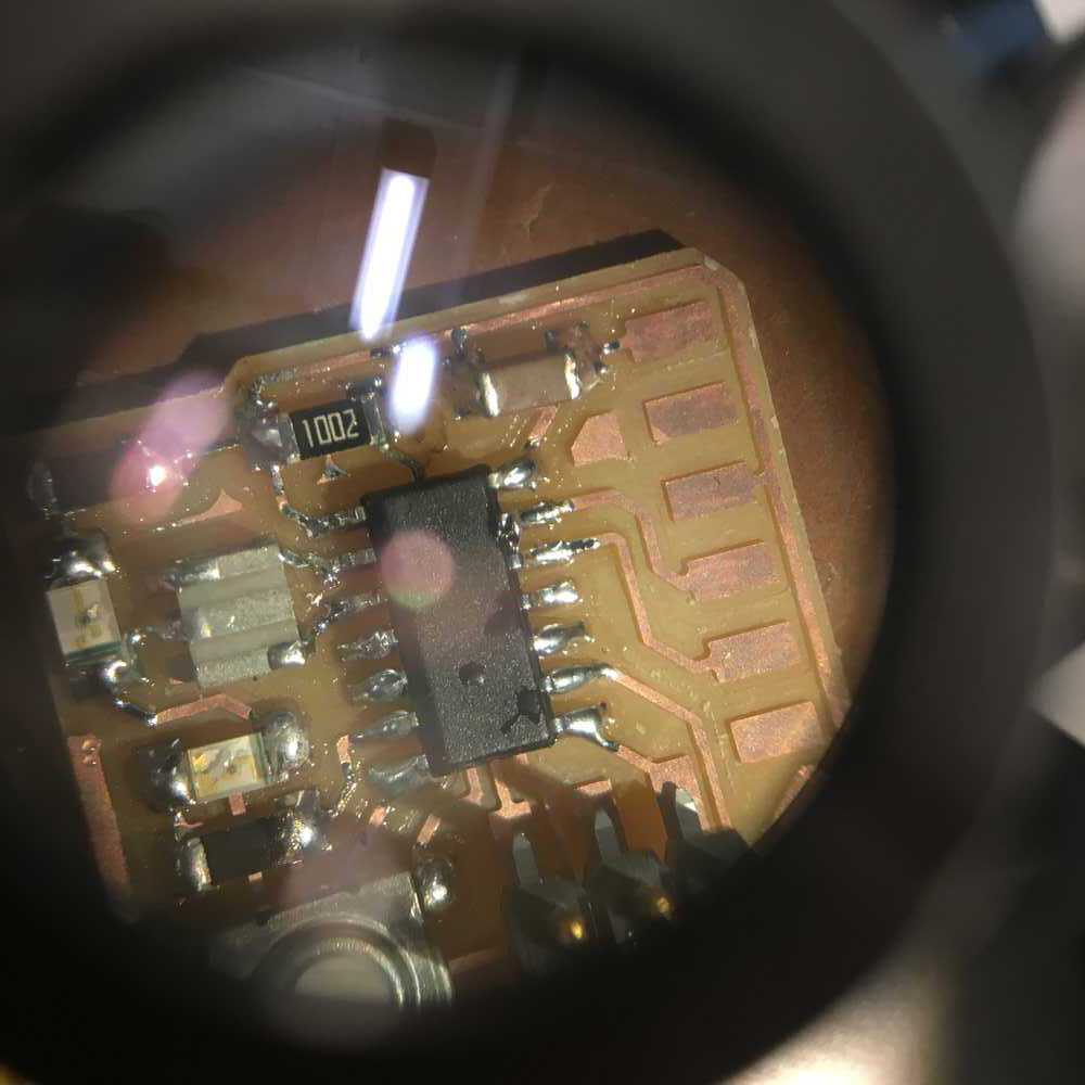
The only mishap was that when I plugged the board into the computer the red LED light (between VCC and GRND) didn't turn on. Everything else worked. I checked the board for shorts with the multimeter and that wasn't the issue either.
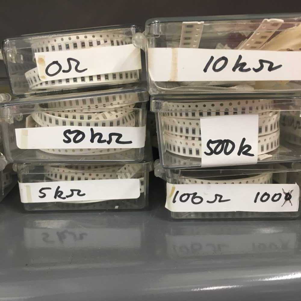
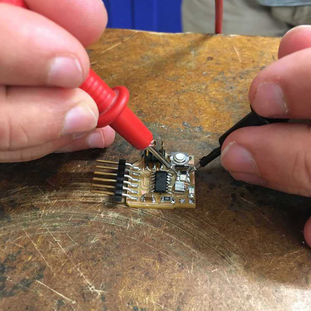
Turns out the issue was that had shaped 500ohm resisters for 500k ohm resisters. Oops. Took them off the board with heat and solder braid.