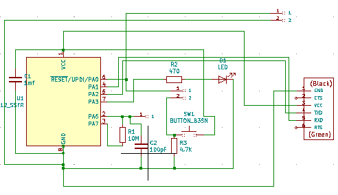
The main idea for me with this circuit design was to have pwm for the LED pin w/ a push button with a capactive sensor (for my final project) and the FTDI output to be able to communicate with the Arduino. I ran out of pins using the ATTiny412, but wanted to make it work so I added a jumper on PA0 that is unconnected when it is being programmed and connected when I want to use the pushbutton.
The components we got in our kits are here
The electronics design information we were given by Zach Fredin and Anthony Pennes is here. And the corresponding video is here.
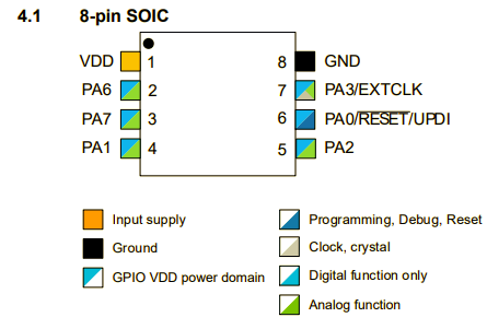
The data sheet for the ATTiny 412 is here and I ateached the pinout below.
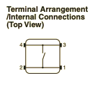
The pinout for the switch is below. I wanted to make sure I didn't confuse myself and put it in the board incorrectly.
My first attempt at a circuit. Then I realized I could make the circuit beter, by adding a few components.
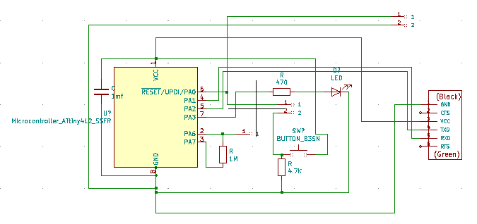
After looking at this Arduino Website I decided to add a 100pF capacitor for stability and change my resistor to 10M ohms to be able to sense a hand 4-6 inches away.
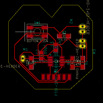
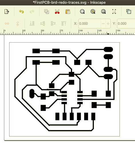
Then it was time to go ahead and route the PCB. The pcb settings were: Clearance-.4mm, Track Width-.4mm, Via Size-1.2mm, Via Drill-.8mm
Routing everything was definitely a pain and took some working to get everything connected properly. Also I learned later on that you can space the traces to make fitting things in and milling easier.
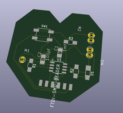
Used the 3D viewer to take a look at my design. Came out pretty well, but some of the routes etc are very close together.
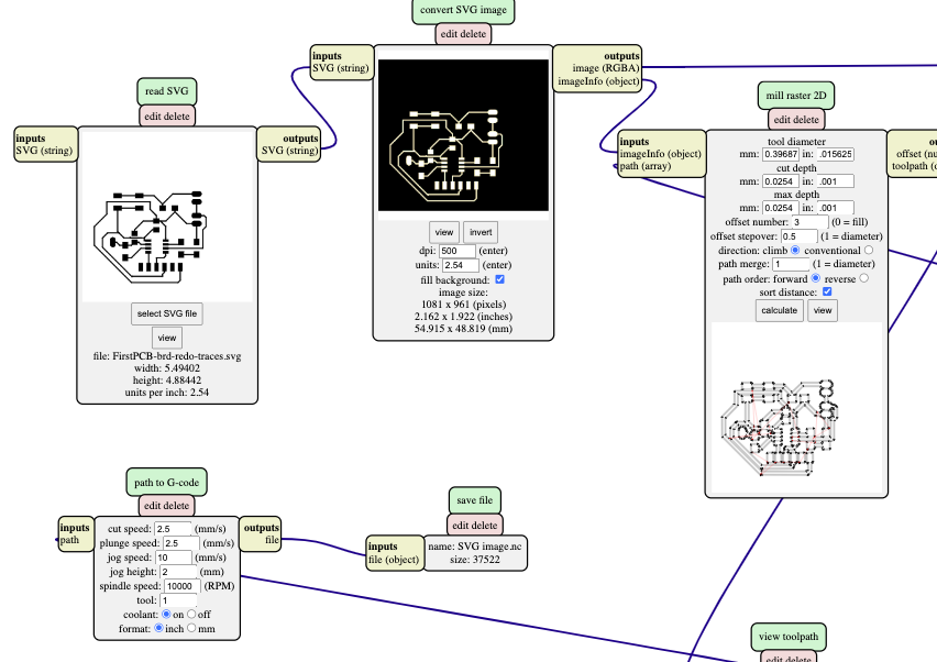
I had to export these layers in order for the svg to have all components I wanted.
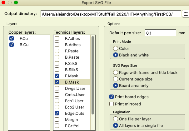
Figuring out this flow took me forever, because I realized that I couldn't use the PNG mods program and then moved to exporting in SVG. I had to seprate the edges and traces in two different layers in order to export. It also was helpful to move everything over to the lower left corner so that the bit wasn't moving super far in the beginning of the cutting flow.
You will also notice that by this time I had given up on the heart and also spaced things out in a cleaner manner.
This is a big oversimplification, because it took me a long time to get to the mods with appropriate files. I wasn't able to use the mods for 2D pcb mill because it's invert feature wasn't working. Therefore I resorted to using the 2D mill mods and just reduced all the values to be the ones appropriate for the pcb mill.
I used the V-bits. I had trouble cutting out the traces, because my bed was uneven and so only parts of it were cutting out. So I had to restart multiple times. Eventually I got a fairly flat surface and went down .23mm (which I think was a bit much)
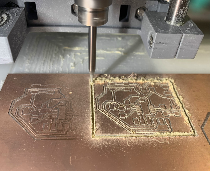
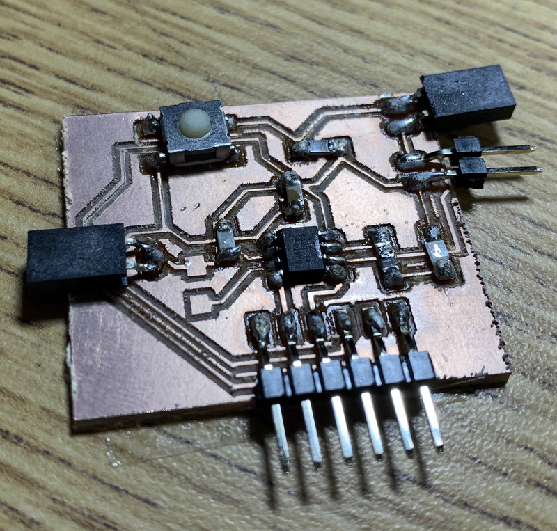
Eventually I got a good cut, but am still wary of all the connections actually being connected. I guess we will see next week. I went ahead and soldered everything. The hardest part of soldering is definitley the first solder for a part. After that the part is fixed and not difficult to solder.