Week 4
Instrument/Programs used: PCB Mill, KICAD
design rules: a set of guidelines for ensuring that your pcb can be made on whatever pcb mill you are using; i.e., if you learned previously the smallest possible size for a trace at 16 mm, then this is a design rule you should check
SMD: Surface-mount device
Week 4 Lecture notes
design rules: a set of guidelines for ensuring that your pcb can be made on whatever pcb mill you are using; i.e., if you learned previously the smallest possible size for a trace at 16 mm, then this is a design rule you should check
SMD: Surface-mount device
Week 4 Lecture notes
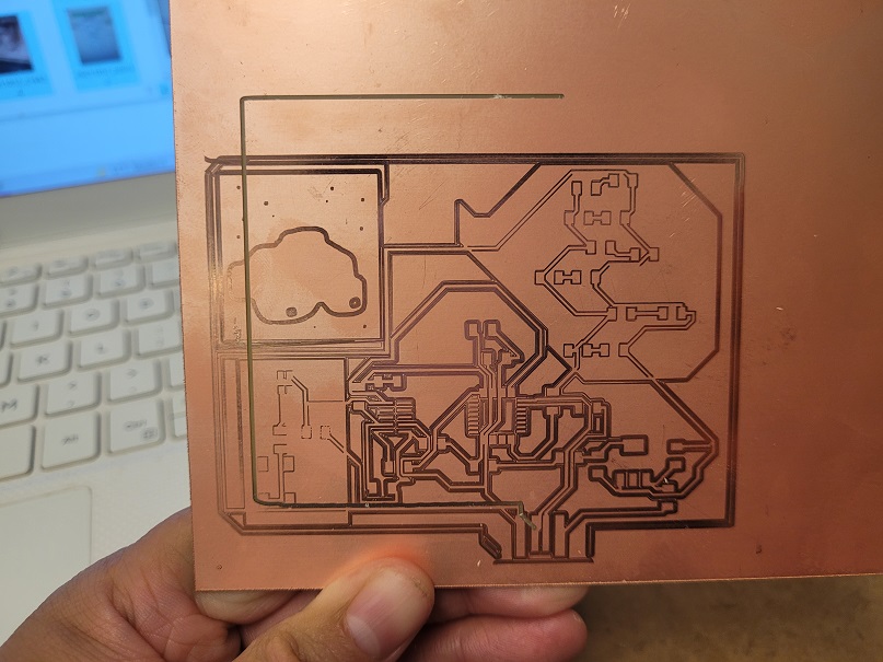
So, first tragedy to note: this week, as I pulled my previously milled PCB , i realized it actually got smushed and the 4-pin connector got crushed, even pulling up some of the copper tinning.
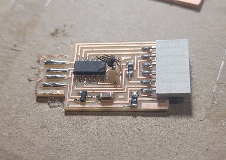
So unfortunately, I didn't get to test them. However, I'll have to make time to remake it soon and I guess the brightside is I will hopefully be a PCB-soldering MACHINE by the end of the semester. Additionally, after chatting with Laura, it's not imperative for this week's assignment (just for future weeks!)
I wanted to break down the boards a bit because honestly I was very confused by the selection and choices. I have some decent exposure to electronic components, but the concept of making my own microcontroller or "designing" your own circuit beyond "connect two wires" was fairly new to me.
The previous board I made was a serial board. This week, we want an echo board.
Neil recommended 3 specific boards during lecture: the ATTiny (hello.t412.echo.) and the 2 versions of D11C echo (hello.D11C.echo.1) and (D11D/hello.D11D.echo).
I'm not sure of the details, but the primary differences in these boards seem to be that the ATtiny doesn't "speak serial," so you would need to additionally make a UPDI converter and a pin converter board (note: I'm not 100% confident on this second adaptor purpose, i'd check with a TA or maybe a later week--the point is, the ATTiny requires two additional boards to properly speak to the d11c serial/programmer).
Meanwhile, the d11c Echo that is just four pins would be doable, but would need to build a four-pin-to-x-pin converter board as well to "talk" to the d11c serial.
At office hours at the CBA, Jack talked about how the SAMD21E would likely be the most useful in the long run, as it had many extra boards. Additionally, his tutorial followed this board. So I decided to follow that.
Group Assignment
So I made sure to attend office hours and observe, even though my board was unable to be tested. However, I did NOT have the foresight to take pictures of the process of someone else's board getting programmed. Laura hooked up another student's D11C-serial board, added a bootstrapper program. This enabled the microcontroller to "learn" its job. Then she added the Echo function, meaning when someone typed into the arduino IDE, the microcontroller would respond (or ECHO!). Laura was very helpful in how to do the assignment. I still had many questions about theory, however.
Redrawing a PCB
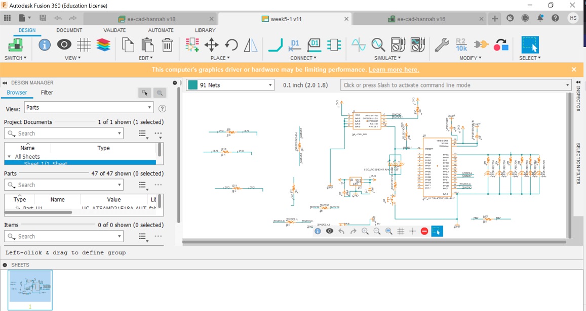
1. Using Eagle: Using the very helpful tutorial by Jake, I bumbled my way through, although I'm not confident on if it's "good" design. First, you draw the schematic. The schematic is a bit more flexible; basically, you lay the pieces down and get an idea of how they're supposed to connect to eachother. Here you also put in any required resistors that each SMC might need.
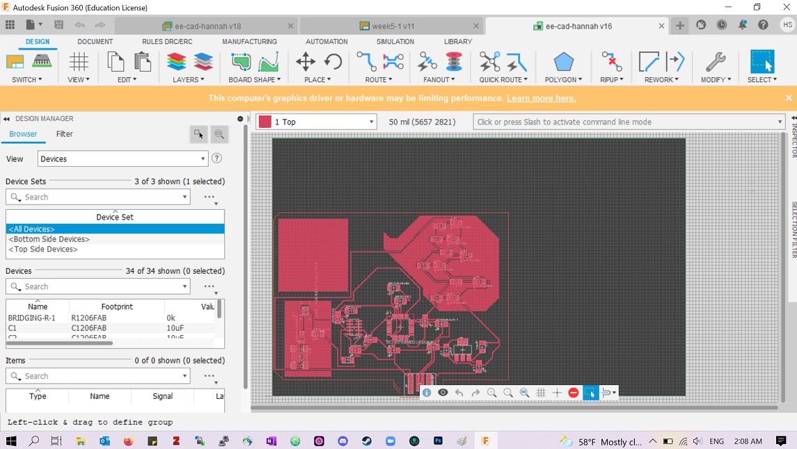
Next, you route it. This is the tricky part and I'd actually recommend attempting to route as you go. I wanted to have several LEDs for my moon, so it got confusing quickly when I had to route at the end. At least make sure to move back and force between the two as you go so you know how each are connected. This was the hardest step and took me almost a whole day.... I had no real sense for how pieces should line up and had to use 0k resistors to "jump" across my board several times, leading to a very unhappy design rule check.
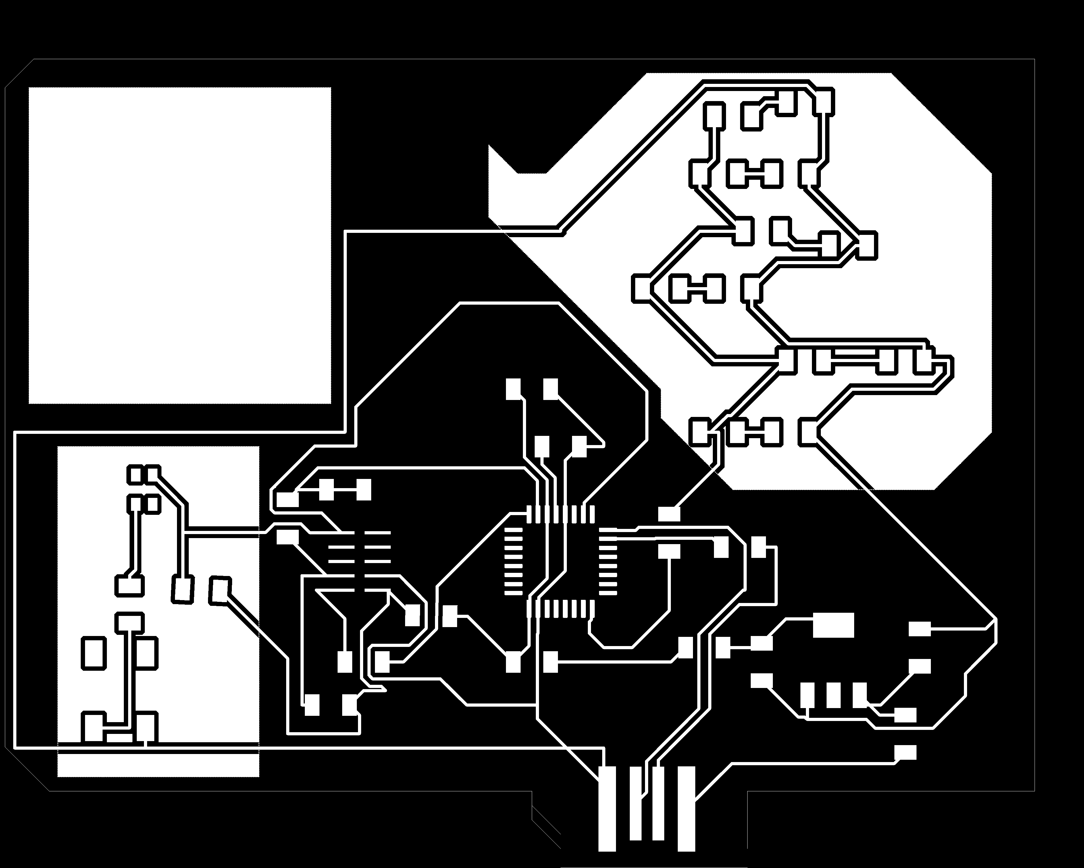
Finally, once it's routed, you'll have to make the PNG to upload to the mods program. This can be done in a few ways, but I downloaded photoshop to try to get some fun design stuff going on.

Milling the PCB
unfortunately this turned out to be a series of difficulties, one after the other. First, I discovered that all the existing boards had been cut to 2x3 inch pieces, which meant I had to resize my board and possibly cut my initial design out.
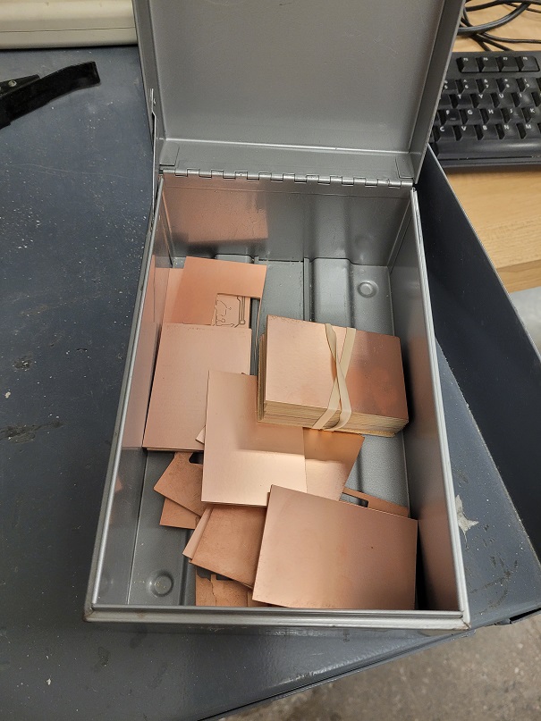
Resigned, I started doing that. However awhile later, one of the TAs came and gave me two larger copper boards. He also noted that I may have some issues with milling the larger boards due to possible bends. This turned out to be sage advice....
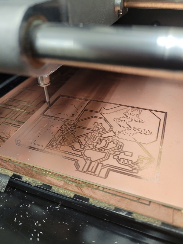
So i taped down my board to the PCB mill, opened my png in the mods program and got to work on the traces. Now, because I couldn't figure out how to combine the PNG of my board from Eagle and the PNG I had drawn of a moon and cloud, I opted to try to instead mill them one over the other. This worked except..........
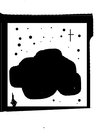
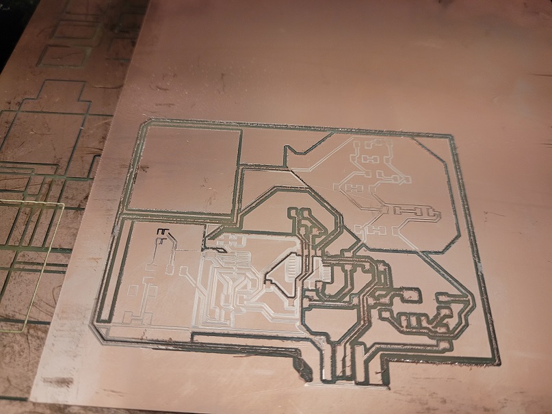
The intended completely milled cloud portion of my board came out.... well, partially done.
I have no explanation as this is the cloud trace portion:
So.... who knows? It's a moot point anyway, because yet another Disaster struck:
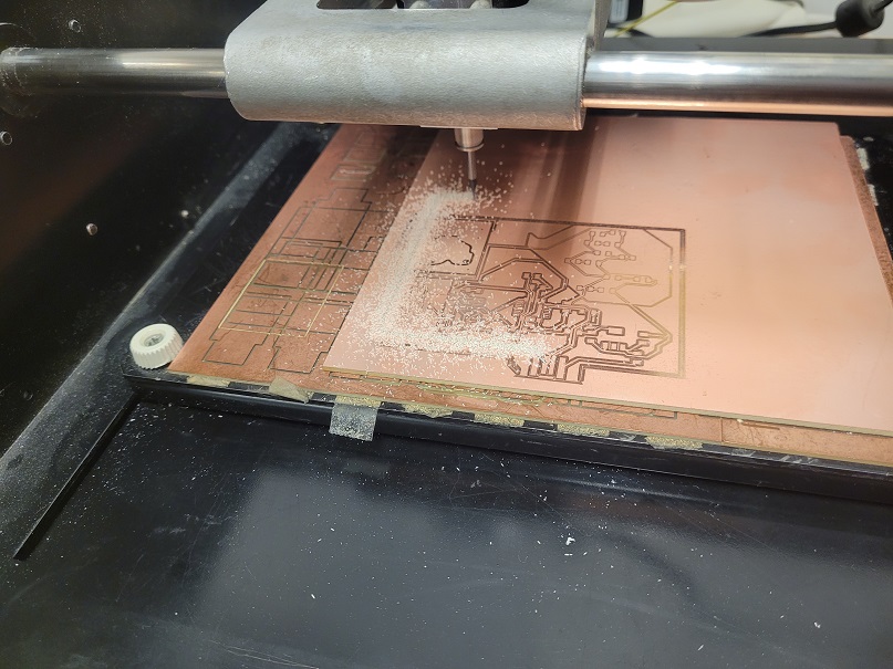
My outline PNG was slightly off from my trace png, causing a cut straight through the switch/LED portion of my traced board.
Honestly.... it was a lesson in patience.
Taking my backup, I taped it all down more evenly and tried again.
And yet................................
I think I will just have to start simple and try again.
As a side note, this week's skill continues on throughout the semester. Designing a board is a skill I struggle with the rest of the semester, but did successfully design and mill a devkit board, which you will see discussed in week 6.
Final Notes and Lesson Learned
1. Avoid using a large copper board. It will lead to sadness.
2. Toggle between your schematic and route boards as you work, to get a sense of what and where your parts are.
3. To those in the architecture section: get started and start going to EECS/CBA office hours as soon as possible. The Archshop staff are extremely helpful, but they don't have as much insight as the EECS TA has about the nuances of PCB design. Although I started working on this the day of recitation, I ultimately was working til the last minute. I spent hours going to different office hours to try to get some insight towards these boards and good design, and found myself working til the last minute.
4. If one week has a lot of learing for you (as it has been for me, especially learning to use EagleCAD), it's ok to start with the basics. A bulk of my time was attempting to learn this program, and getting too ambitious with my design meant I had less time to troubleshoot the actual milling of my board.
5. Think about the questions and ask the appropriate person. I had a lot of questions about the microcontrollers and some theory, and should've gone straight to the EECS office hours to ask.
6. Neil said this week's goal was to learn how to design, not understand what yuo're doing.