For this week's assignment we learned to familiarize ourselves with a software environment for PCB design, design a PCB with it, and manufacture the PCB. For my PCB design, I chose KiCAD as a platform. The PCB I designed features a SAMD11 microprocessor connected to a button and an LED as well as a 10-pin header to be used as a SWD interface for bootloading in week 6.
2. Installing the fab Libraries
3. PCB Schematics and Layout
4. PCB Milling
4. PCB Stuffing
Introduction to the PCB Design Process
The two most commonly used software environments for PCB design are KiCAD and EAGLE. Both are conceputally very similar in how the PCB design process works, and are mostly different in their interface implementation of the process. For this class, I chose to familiarize myself with KiCAD. When working on a project in KiCAD, the following main screen is available, which I will use to briefly introduce into the key concepts of PCB design:
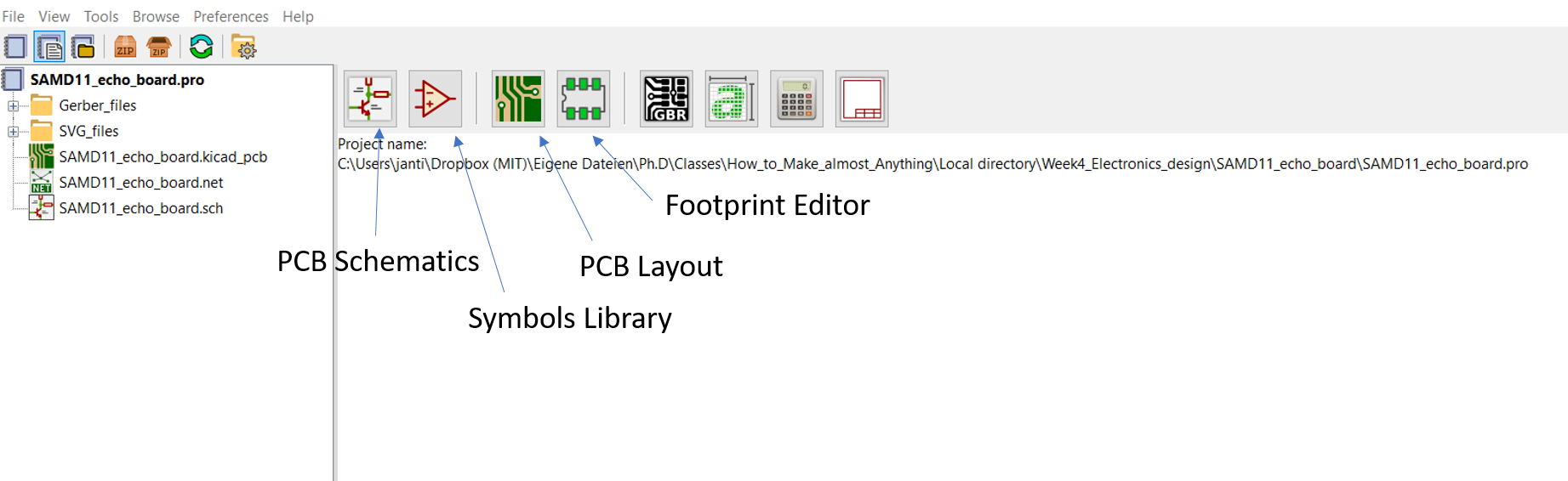
The two main editors that we will work with are the first and third highlighted symbols above: the Schematics Layout Editor and the PCB Layout Editor . The Schematics Layout Editor is the one used first in order to determine which electronic components are to be used on the board and how they are wired together. Electronic components are represented by Symbols in the Schematics editor and can be found in the Symbols Library . A Symbol is a representation of an electronic component schematically depicting the number of ports/pads, ideally sorted by names, available to connect wires to. The symbol by itself does not represent the physical layout or dimensions of the component. This is done by linking a symbol to a Footprint . A footprint contains the physical dimensions and geometric arrangement of each pad/connection on an electronic component, as they are visible in the real world. If not available in pre-existing libraries, these can be created by referring to the data sheet of a new electronic component, looking up its contact pads' physical dimensions, and creating a new footprint in the footrpint editor using these dimensions.
Once a PCB schematic is created, the schematic connections made therein are used to create a netlist, a file containing the information of how the symbols used in the schematic are wired together; the wires being referred to as nets. This leads to the last step of the PCB design process, the PCB Layout Editor , where now the footprints, that is, physical representations of each component, are imported alongside the information of how they should be routed, that is, connected together. The components are then moved around until a layout is found that allows a minimal amount of tracks (that is, connections between components) to be used. Once all connections are routed, an outline for the PCB is added, and the design files can be exported into an appropriate file format, depending on the desired manufacturing method. For professional board houses these are typically so called Gerber files that contain information on each PCB layer in a separate, at the very least usually front-Cu and outline for a one-sided PCB. Additional files may contain information on back-Cu for two-sided PCBs, or drill files for mounting holes.
For Neil's mods software, export to SVG or PNG is used for board manufacturing.
For the details of implementing above outlined concepts in either EAGLE or KiCAD, Youtube provides many excellent tutorials!
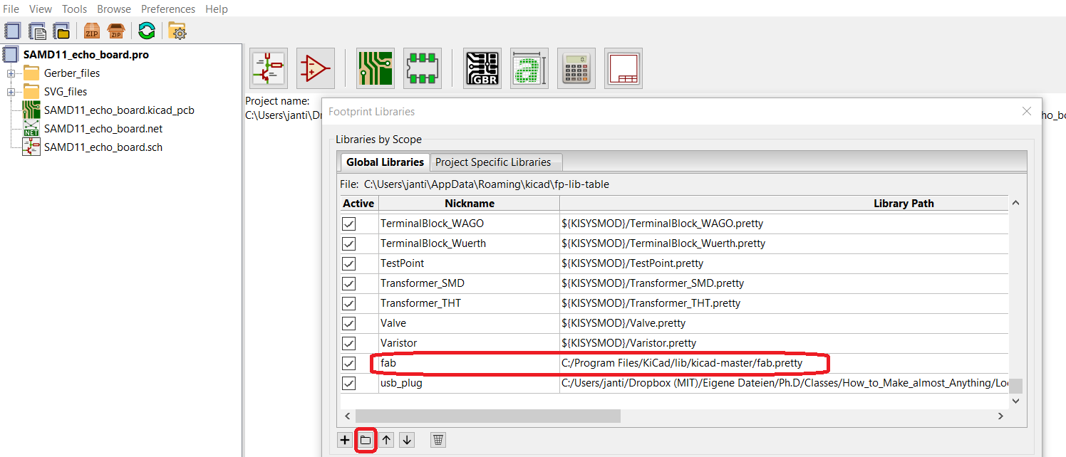
Installing the fab Libraries
The symbol and footprint libraries of the electronic components used in the fab lab inventory available for this class can be downloaded here. In KiCAD these are installed by going to Preferences and then Manage footprint/symbol libraries.... Under Global libraries simply click the folder symbol and add the .lib file under kicad-master for the symbol library and the .pretty file for the footprint library. These will then appear in the list as shown below.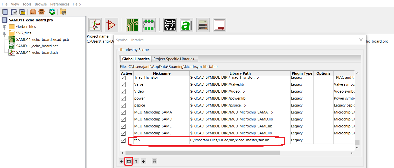
PCB Schematics and Layout
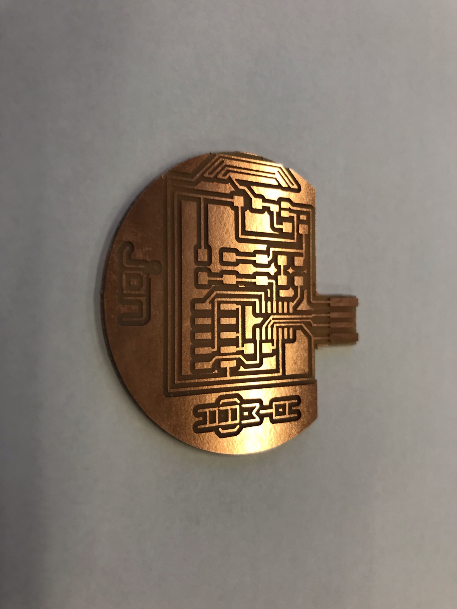
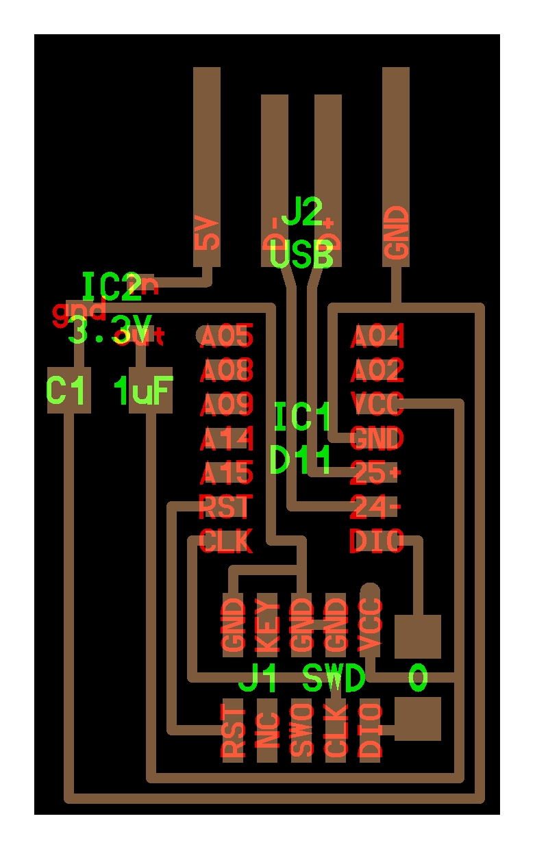
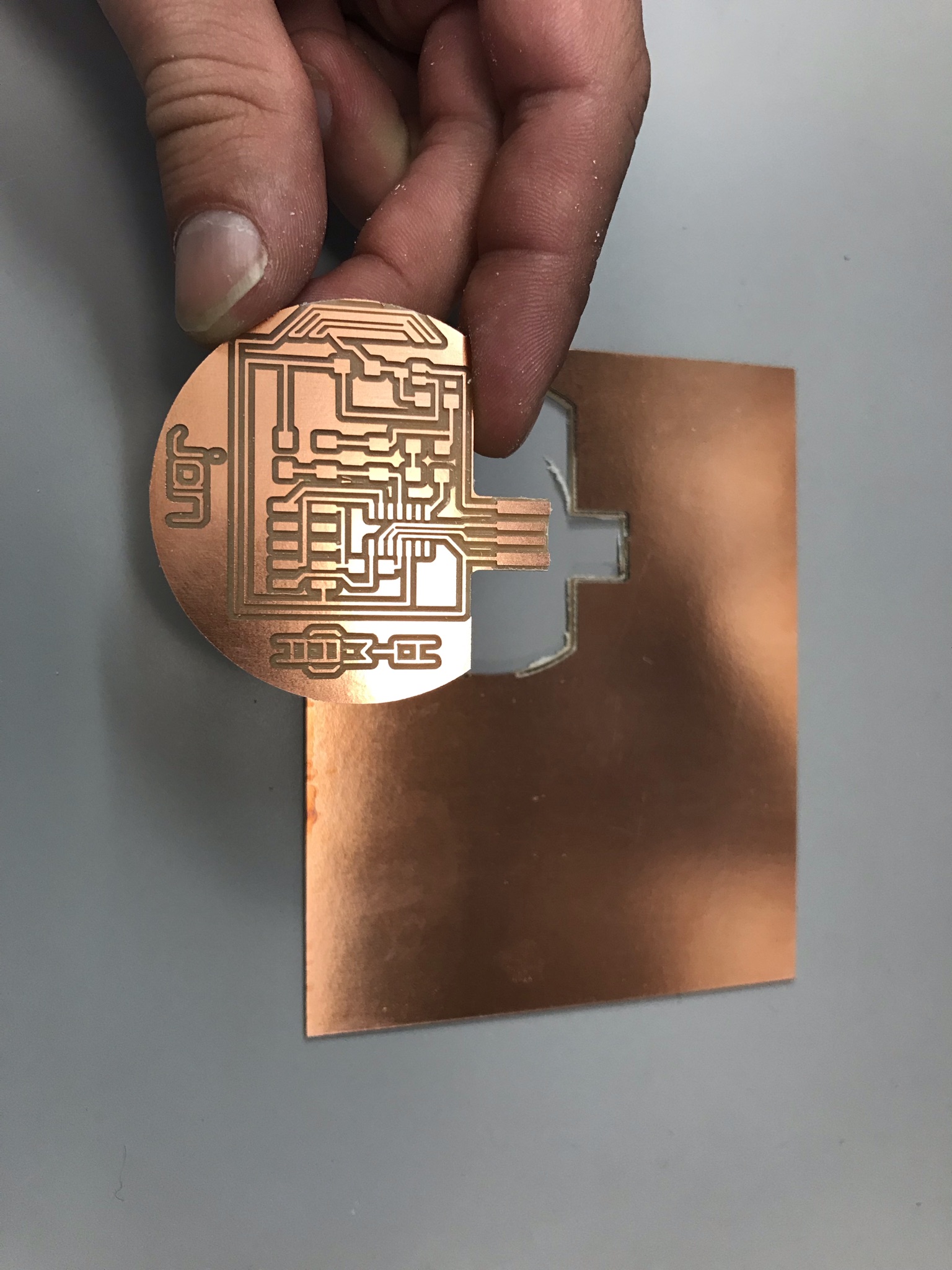
Starting from Neil's hello world echo board featuring a SAMD11C microprocessor, as shown below, I designed my board for this week's assignment.
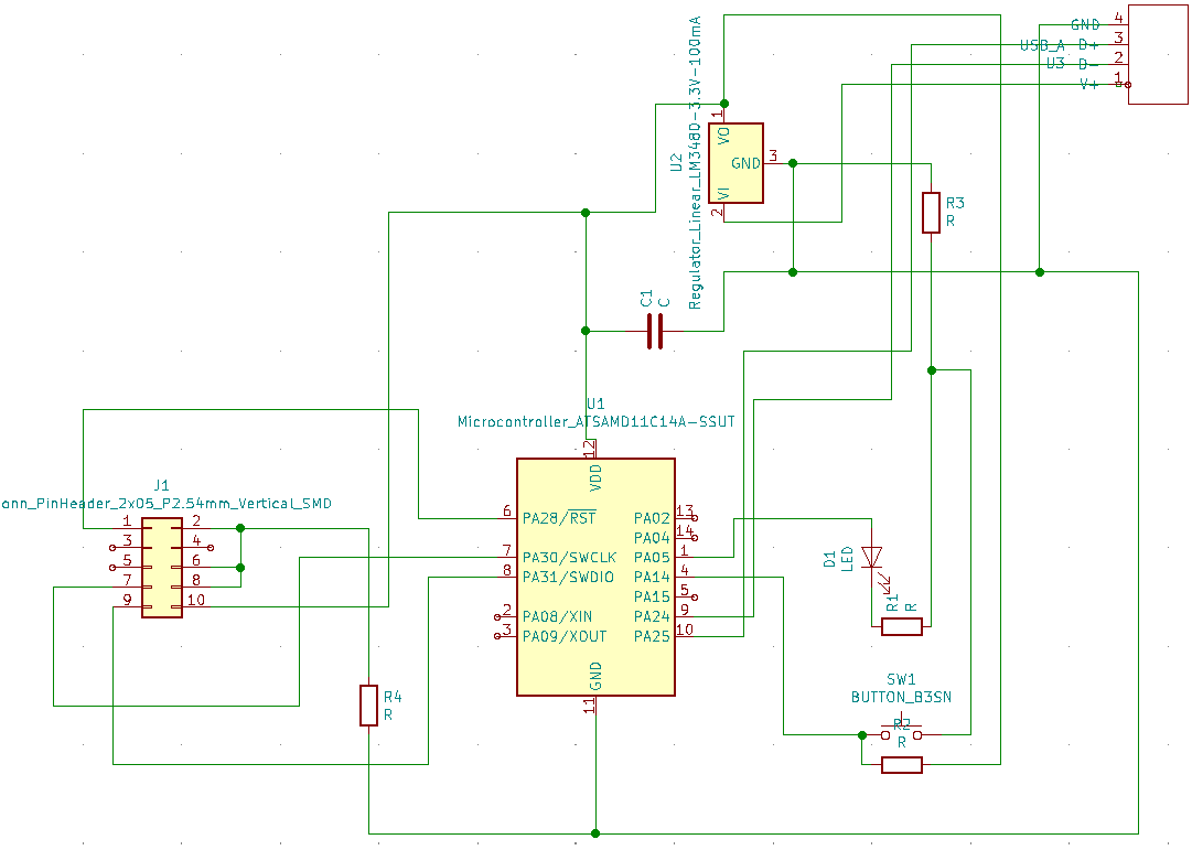
The PCB schematics on the left show both an LED and a button connected to pins on the SAMD. The LED is wired in series with a resistor for current-limiting so the LED does not burn out. The push button is connected to a pull-up resistor which prevents floating of the button when not pushed. This button will thus be read as LOW when pushed, and HIGH when not pushed. The 10-pin header on the left is a SWD interface used for bootloading as will be explained in more detail next week. The 3.3V regulator in the top is fed with 5V from the USB connection, and regulates those down to 3.3V which is the voltage the SAMD11 requires to run (it will burn out at 5V). C1 is a capacitor placed between voltage and ground near the voltage regulator to compensate for fluctations in voltage ouptut. R3 and R4 are 0 Ohm resistors that are used in the layout as jumpers to connect two pads that cross over a track in my layout. Since two tracks can of course not cross without creating a short circuit, to resolve this one can a) first try to re-arrange components more efficiently, b) create a via (a through-hole) to the backside of the board and make a two-sided board, or c) use a 0 Ohm jumper resistor that allows running a track between its two pads.
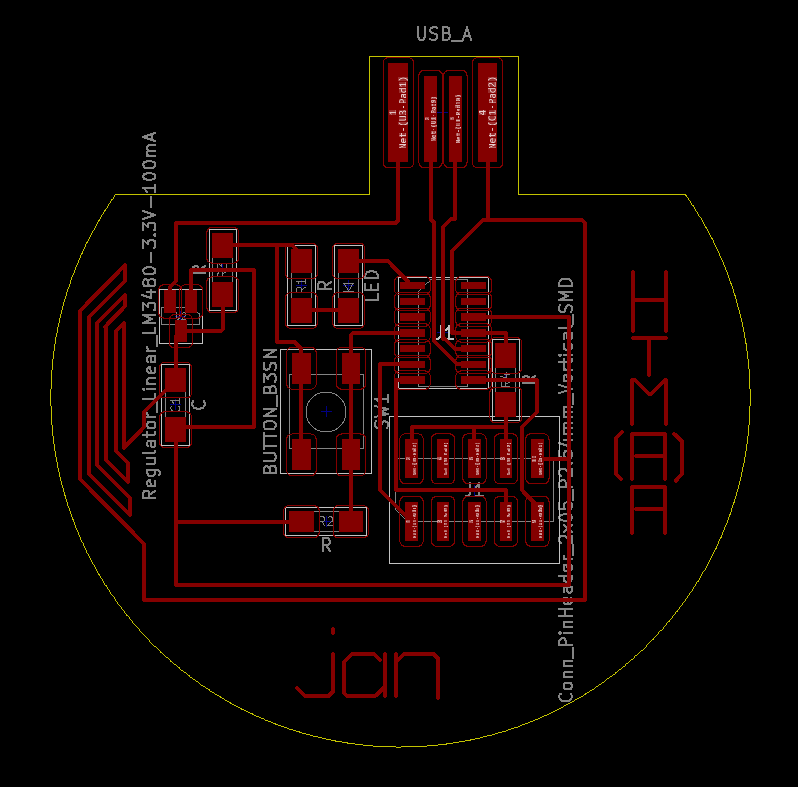
The PCB layout on the right-hand side shows the physical arrangement of footprints on my board and the use of 0 Ohm resistors described above. The wound tracks on the left have no function and were simply put there for fun aesthetic purposes.
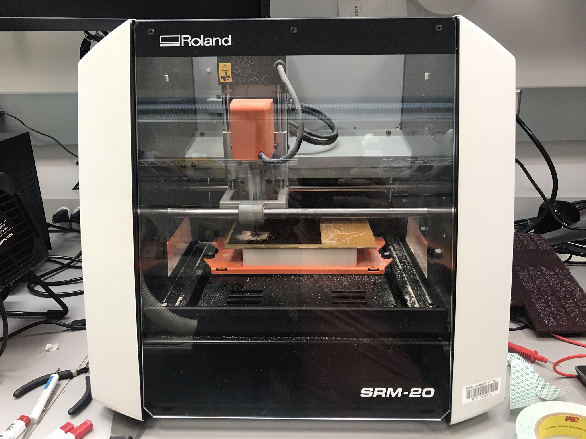
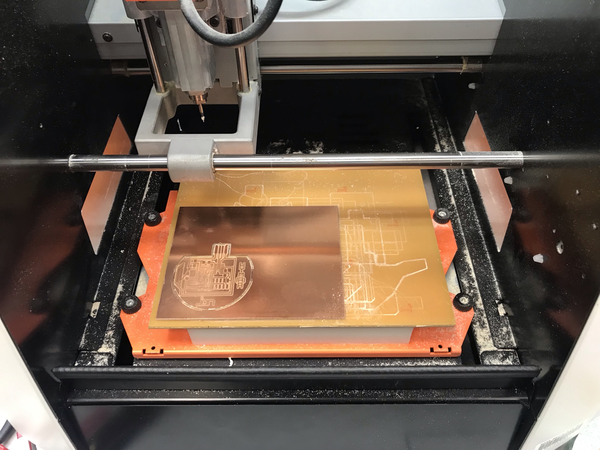
PCB Milling
PCB milling was carried out on the Roland SRM-20 PCB mill using a 1/32 inch flat end mill for coarse milling and a 1/64 flat end mill for more narrow sections. The substrate for PCB milling is FR-1 phenolic resin stock with a layer of copper on top that can be milled into. SVGs of my front Cu traces as well as the board outline were imported into Neil's mods and used to send the job to the PCB mill.

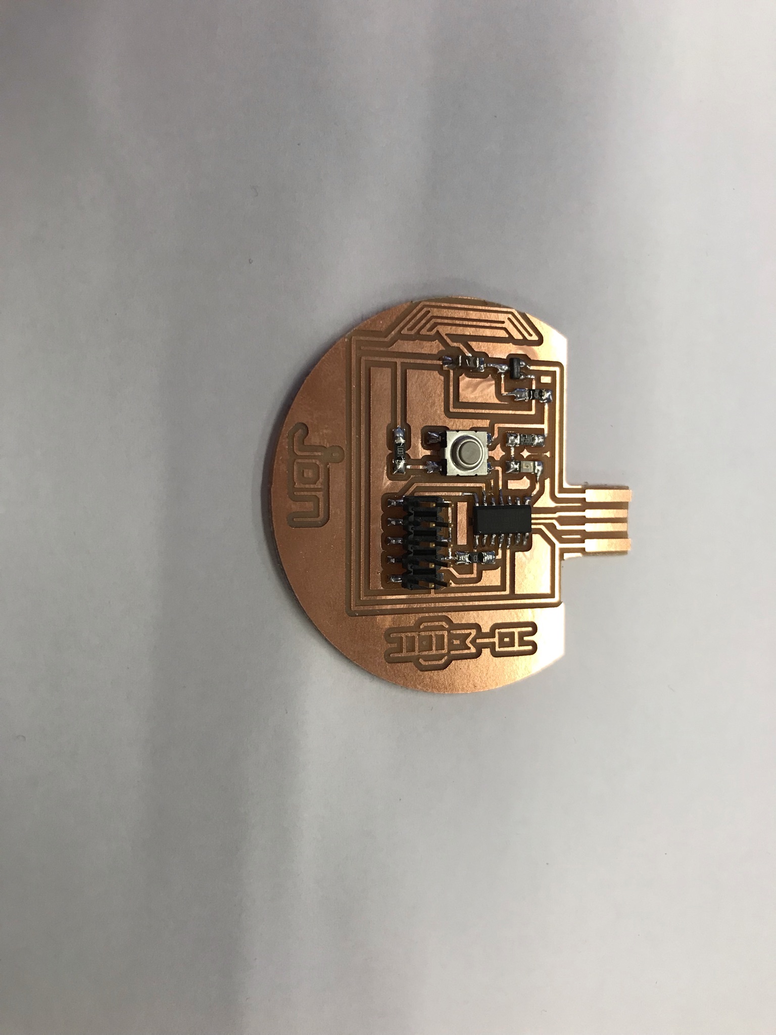
After milling the finihsed PCB can be separated from the FR-1 stock for stuffing.
PCB Stuffing
The cleaned up PCB before and after stuffing, that is, the soldering of electronic components onto the board.