
Got a bit of a late start this week, and wasn’t able to start working on this until Sunday afternoon. So I wasn’t super ambitious.
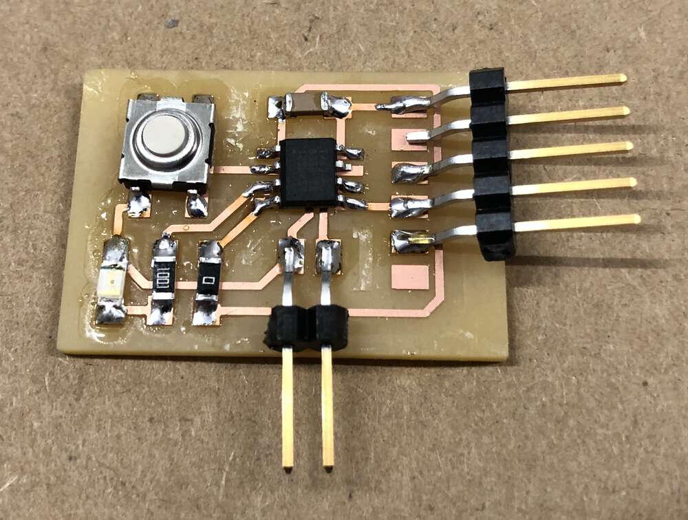
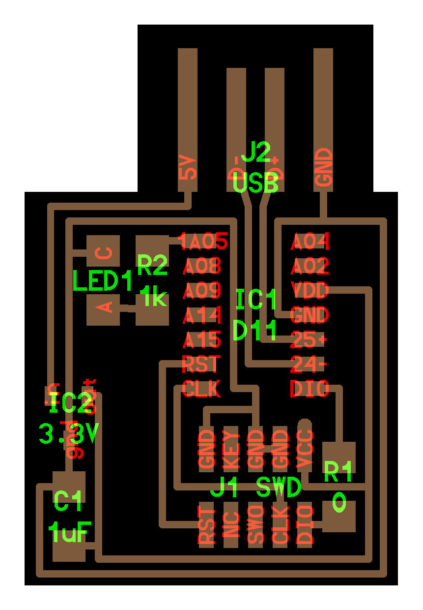
I was hoping that issues I ran into during Week 3 would actually give me a leg up. I wasn’t able to get my programmer working, so I decided to make a different board and make a (successful!) blinky. Which means that I already have set up an LED.
As a warmup, I decided to recreate that D11C blinky in KiCad, just because I was already familiar with the layout. And I’m glad I did! Because I learned a bunch of things to be mindful of.
The schematic went pretty smoothly. The Power_GND label was super helpful. It took me a sec to figure out the logic around the capacitor getting to ground, just because the schematic of that feels quite removed from the footprint.
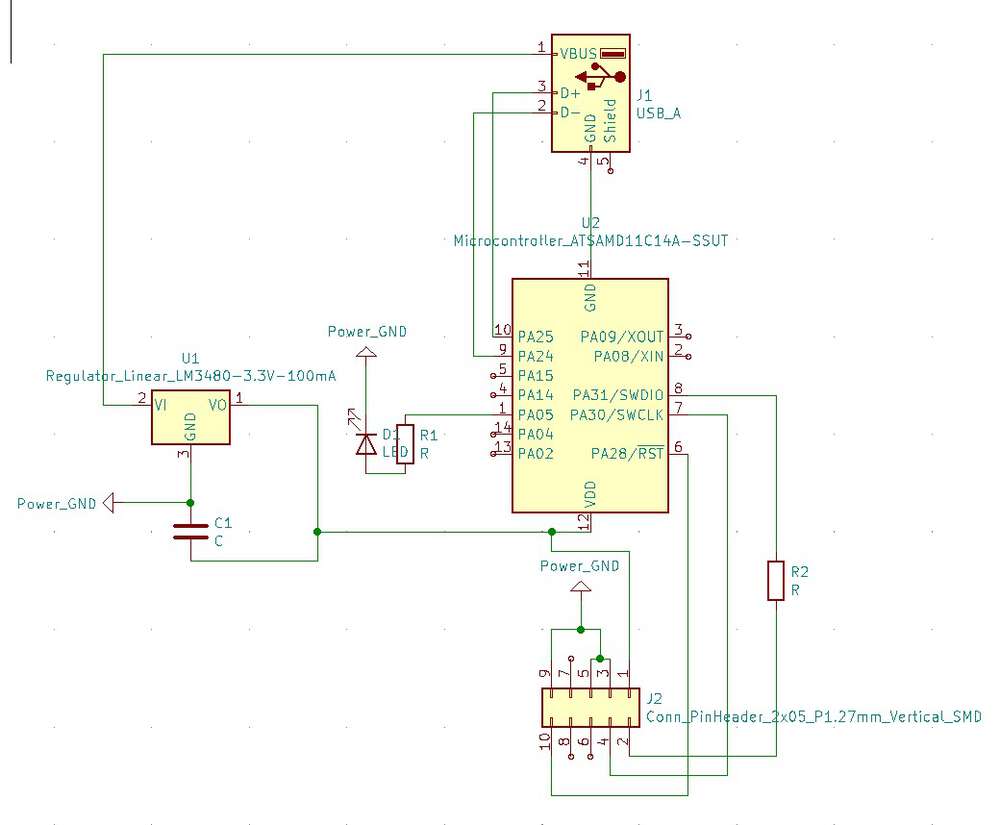
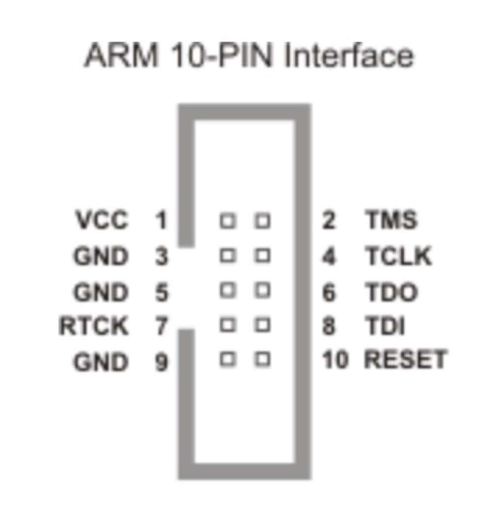
The fab schematic for the 2x5 connector is unlabeled, but it was pretty easy to find schematics for ARM 10-pin interfaces online.
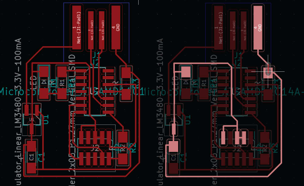
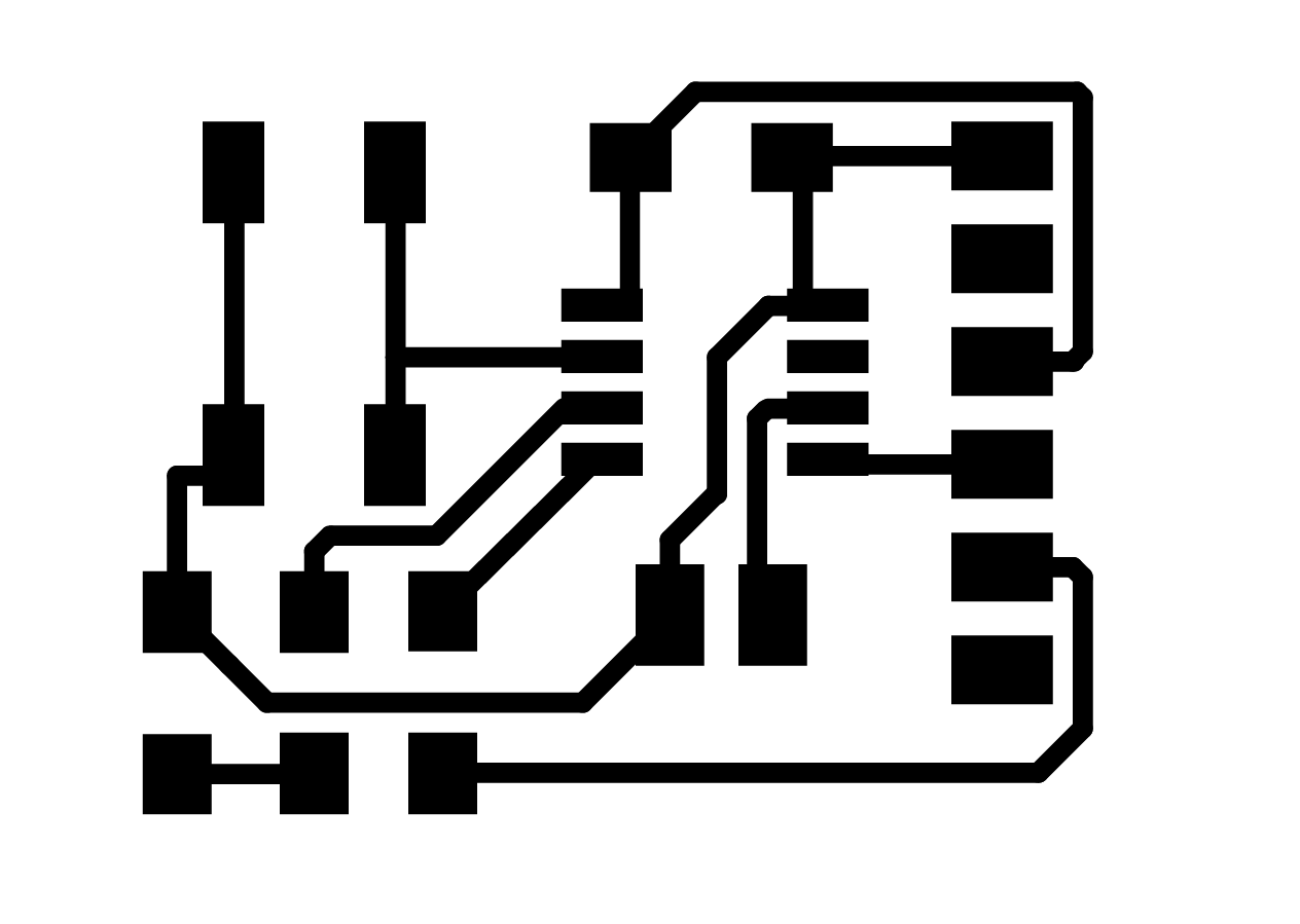
Laying out the PCB was more of a challenge. I was using 0.5mm for both my tracks and clearances, which was Zach’s recommendation during recitation. But that made it totally impossible to snake four traces underneath the microcontroller, which is how it looks on the example board. I also couldn’t send a trace underneath the regulator.
Basically, I learned to be careful about trying to match the example boards that Neil has already made. TA Rob told me that he’s using narrow traces, and also using alternate, smaller footprints for components.
I dropped my trace width to 0.25mm and my clearance to 0.4mm, both minimums. And I was able to find an alternate footprint for the regulator, but not for the microcontroller. With these changes, I was able to mostly match the example, although I could only get three traces under the controller and I had to add a jump resistor to get that fourth ground trace cooking. Look at my nice ground path! Don’t look at my sloppy labels.
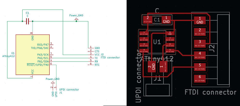
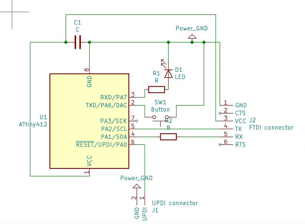
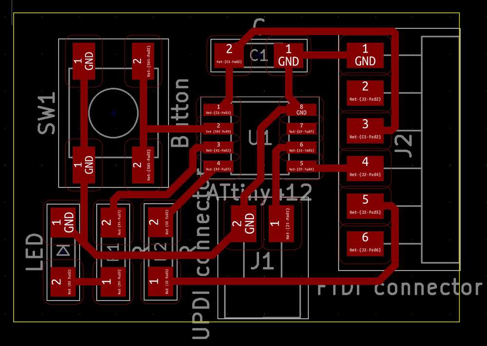
Ok so now for the actual assignment. I decided to start with the Tiny412 echo board with added LED and button.
Laying out the echo version was fun. Despite a sort of janky looking interface, I actually find KiCad quite easy to use. It reminds me of QGIS, which is the chunky open source software I’m most familiar with. I also took labels more seriously this time so they didn’t clunk everything up.
For a while on Sunday night I was thinking that I was going to try to connect my button and LED in a circuit, so the button controlled whether power went to the LED at the hardware level. But I didn’t really know how to do that, and also I realized that it was sort of antithetical to the workflow I’d eventually be using in this class. I’d rather connect all my components to the microcontroller and handle all my logic in software instead of hardware.
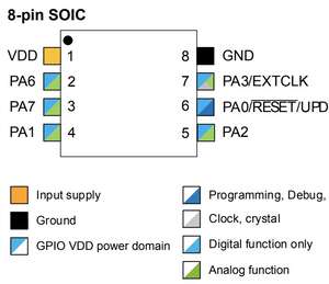
I still had to figure out how to actually connect the button and LED to my microcontroller. Looking at the echo board example, I realized that ports 6 and 7 were open. Looking at the data sheet for Tiny412, it looks like ports 1, 2 6 and 7 all were the same, so I figured they might be interchangeable for random components.
I double checked against Nadieh Bremer’s extremely detailed documentation for her own experience with HTMAA (I admire her data viz work), and saw that she was taking a similar approach. So ports 6 and 7 it was. Here was my final schematic.
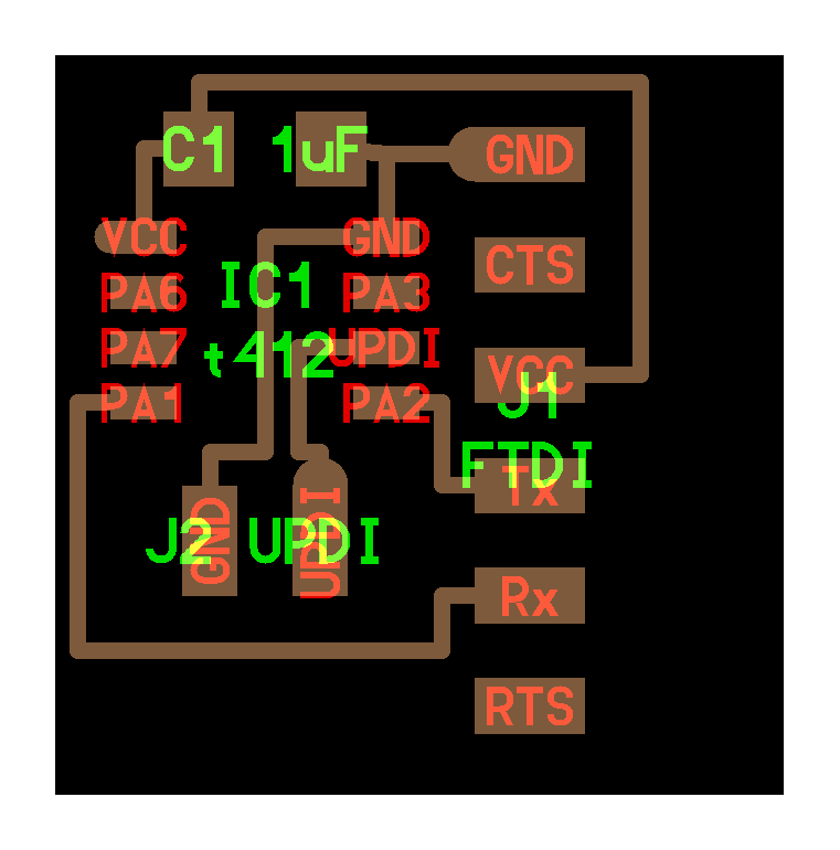
I laid out my PCB, and spent a lot of time trying to figure out if I could route my traces in 1D without a jump. Here’s where I got to, with one missing ground route. I’d switched back to the 0.5mm trace/clearance recommendation.
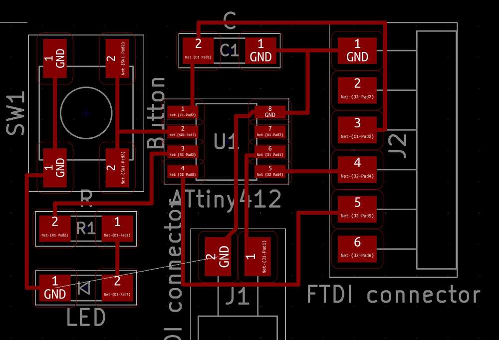
Eventually I gave up. I’d love to learn more about the topology/networks of circuits so those situations would be more immediately apparent. I ended up adding a single jump resistor to make it work, and was quite happy with the final output. I was boring with my outline, and drew a rectangle.
I initially exported my layers SVGs, which was the workflow that Zach laid out. I realized this meant that everything was easily editable in Illustrator, which is a program I know really well. I didn’t end up doing anything crazy, but I did clean up some paths that were bothering me.
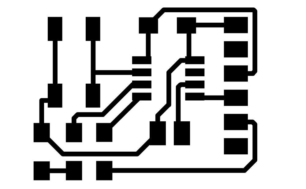
On Monday, on the advice of my labmates I exported them as PNGs instead (I went with 1000 DPI). My TA Nathan took a look at my logic and said that it seemed ok. So it was time to mill.
Remembering tribulations from Week 3, I made sure that my board was pressed down tightly, and that the 1/64 bit was pressed down snugly at the start of the cut. And it came out really clean, but I made a totally new mistake – my copper layer was flipped. Whoops!
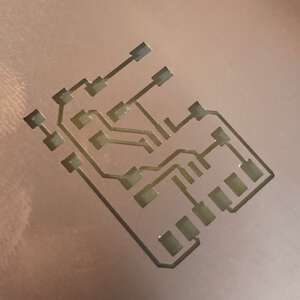
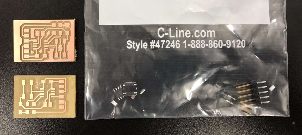
But I fixed it and was able to get a clean board. It had a lot of leftover copper, so I decided to make a backup board with an offset of 6 instead of 4. I messed up on the first one of these (the board wasn’t adhered enough and it bounced) but eventually I ended up with two nice looking boards. Two out of four for milling is frankly a pretty good run for me.
I collected my parts, and made one slight adjustment. We were out of six-pin male FTDI connectors, but I realized I wasn’t using the bottom pin anyways. So a five-pin worked fine. For completionist sake, I also razor bladed all the extra copper out of one of my boards.
Tuesday afternoon it was time to solder. I hadn’t touched a soldering iron for two weeks and I felt it, I started with my microprocessor and couldn’t get anything going. I switched to a different iron and had much better results, sometimes that’s all it takes.
Compared to two weeks ago, I felt like I had a much easier time placing the tiny components like resistors. So progress on that front. I also worked smarter not harder, and left a microprofessor pad and FTDI pad unsoldered because they weren’t actually connected to anything.
Overall I’m pleased with the progress of my joints, and the fact that I finished in ~1 hour 15 minutes. Here’s my spiky little guy.
On Tuesday night I took my board to get tested. There was a little line to get Rob’s help, so while I waited I used the multimeter to perform a beep test on my board. With the caveat the signals passed through a microcontroller can be misleading, I was able to confirm that my grounds were all hooked up correctly. Gabby took the lead on the group assignment and wrote out a more complete assessment of the testing tools.
Gabby was also able to help me start testing my board. She already had the Arduino IDE running on her computer, which I still need to do. We were able to hook up spiky to a programmer board, and, as a test run, install a blinky/button script. I still have a lot to learn about making PCBs, but I was able to identify the UDPI, ground and VCC pins we needed to use for this operation.
And it worked! Here’s my LED light permanently on, unless you hold down the button.
Echo did not work, unfortunately. The program loaded but it wouldn’t echo after we connected the FTDI for serial communication. This was probably a config issue somewhere, because Gabby’s echo board (a Tiny1624) also stopped working.
I waited patiently for Rob to free up, and I learned that even without that mysterious config issue, the echo we installed from Gabby’s computer wouldn't have run. We looked at the echo code for the Tiny1624 and thought it must be identical for the Tiny412.
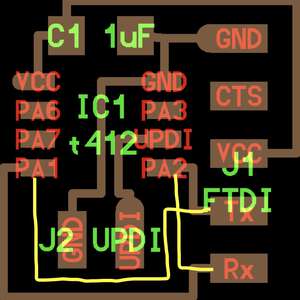
But there is a difference! The echo board example Neil drew up for the Tiny412 actually reverses the RX and TX ports. So the Tiny412 program has an additional line of Serial.swap(1) to trigger that alternate setup. The traditional setup would have looked like this, which I assume Neil didn’t do because it would make the routing on this very simple board a pain in the ass.
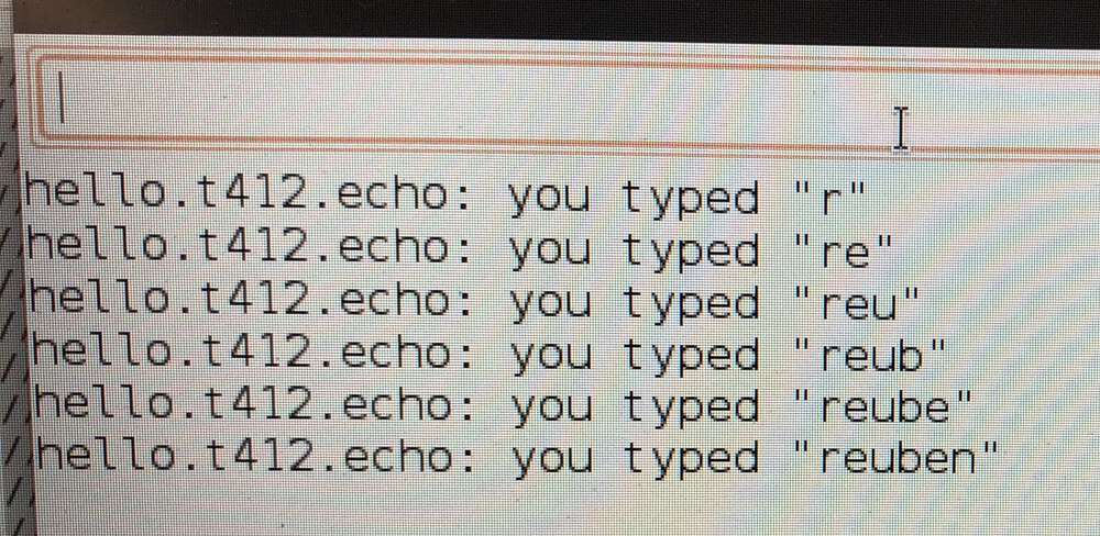
On Rob’s machine, and running the correct Tiny412 echo program, everything worked great. Here’s me getting to echo.
Files: Here’s my KiCad project for my Tiny412 (zipped), plus the final PNGs for my traces and outline that I sent to mods.