for input week, i want to play with light.
• create signals with photo transistors.
• harvest energy from a solar panel.
OP520DA phototransistors in archshop
1206 pad, similar to an LED to hook up.
the opaque lens seems to work within a narrower range of light wavelength.
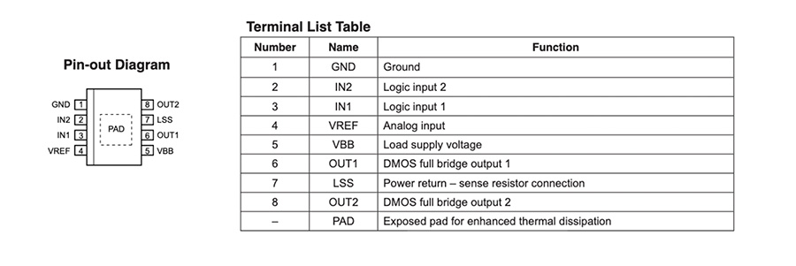
A4950 driver pinout
for output week, i want to work with motor drivers. these available drivers in archshops:
• ZXMHC3 - drawer labeled "MOSFETS (OLD)" - can't find package in eagle library
• A4953 - 40V 2A (8 Pin)
• A4950 - 40V 3A - same SOIC package
• A4982 - microstepping
reference of fabacademy project using A4950
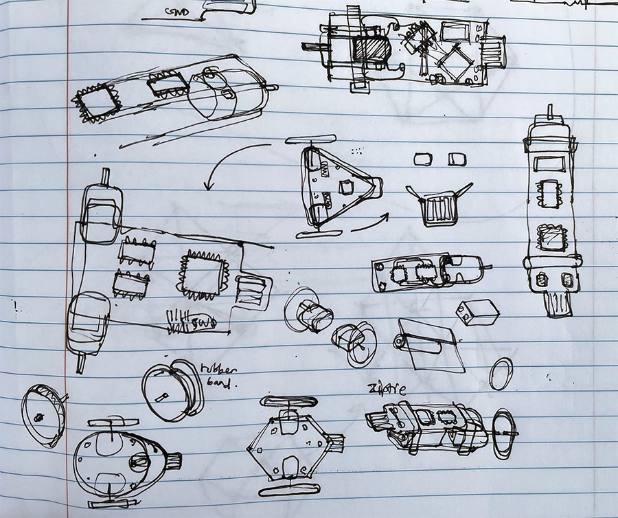
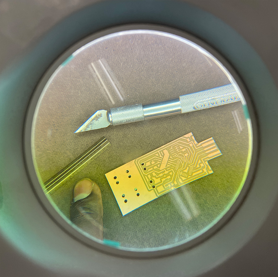
beam bot concepts - pcb as chassis
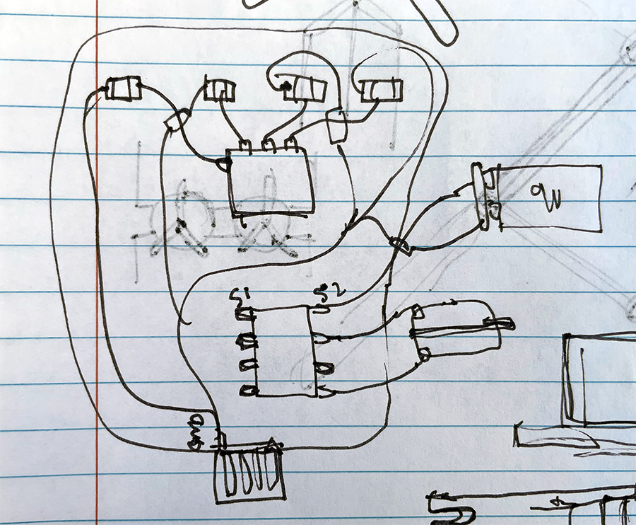
phototransistor and driver on same board
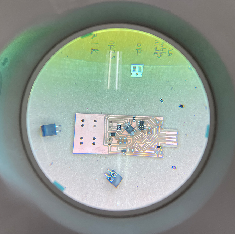
board design
i'm inspired by junk bots / beam bots.
particularly solar engines or solar harvesters.
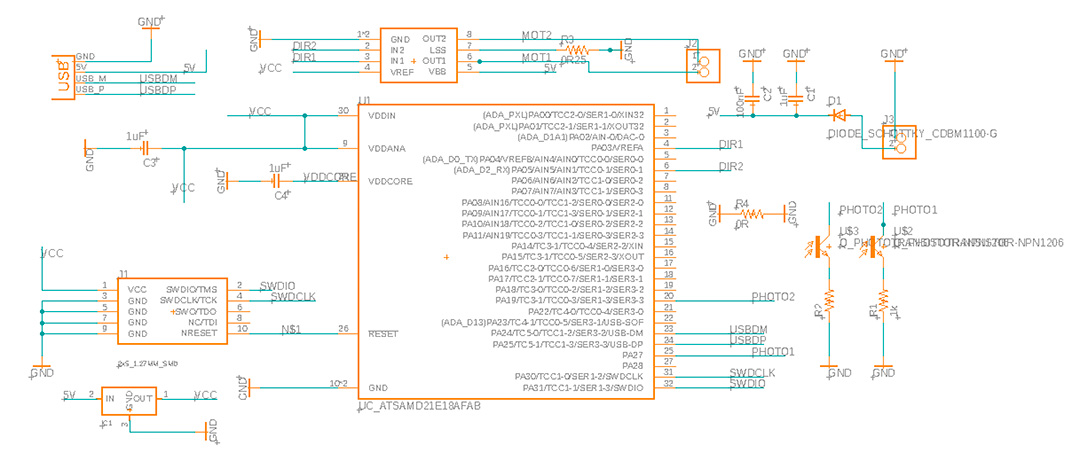
• SAMD21 mcu
• h-bridge / mosfet driver
• JTAG / SWD
i want to consider mobile power supply
such as solar panels and capacitors
questions:
• how to adjust pwm in c++
• how to design in a solar panel as external power supply
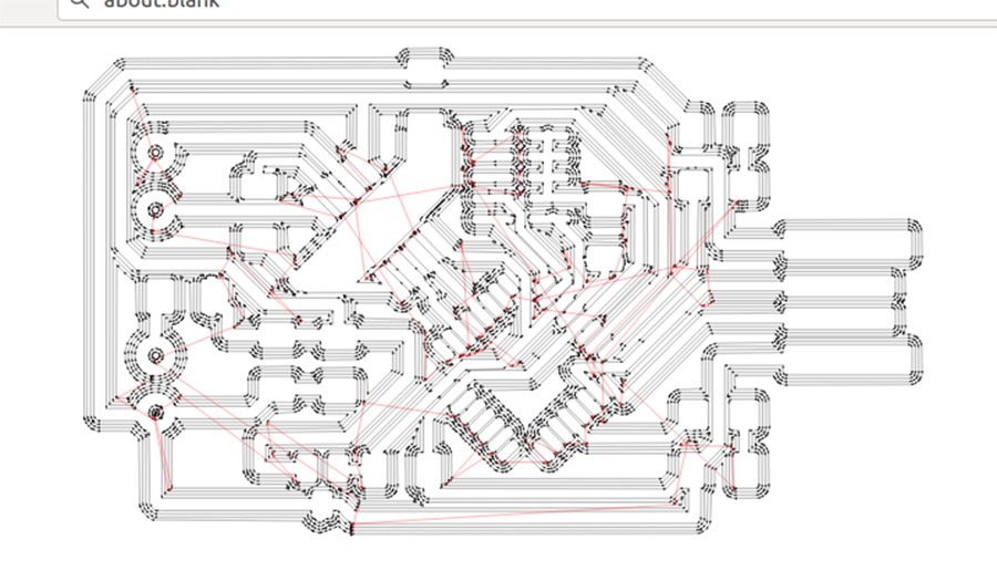
• how to route input, mcu and output into same board?
"ph-driver" schematic
to do:
• cut 3.3V vcc line for JTAG SWD
• move photo transistors onto mcu side of board
• place driver ic's on far side of board
• SAMD21 pwm pins - not 2, 7 or above 13
couldn't find the specific drivers in the fab library,
so i found a 8-pin SOIC packages, use Search in libary manager
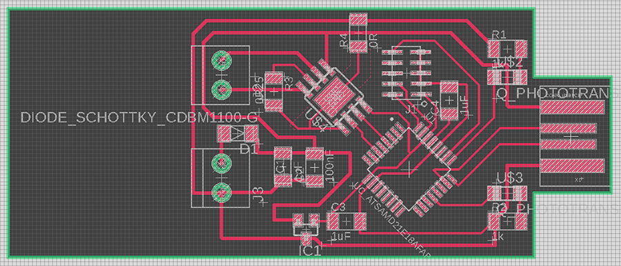
"ph-driver" layout
note: illustrator artifact

adjusting via hole size
made a mistake with my first board
export dpi was 150, not 1000
terminals for motors need holes or vias
i used illustrator to size some extra holes
wrong dpi
1000 dpi
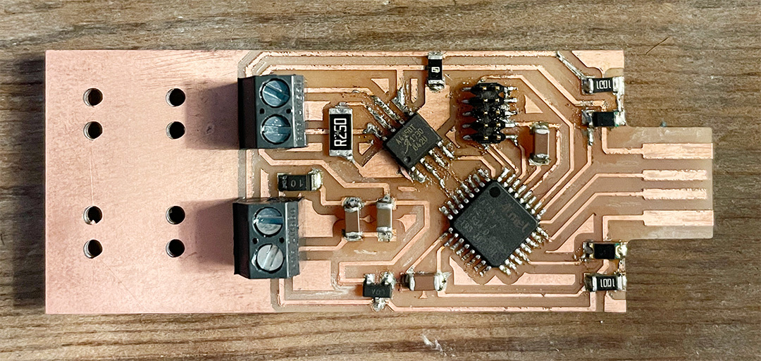
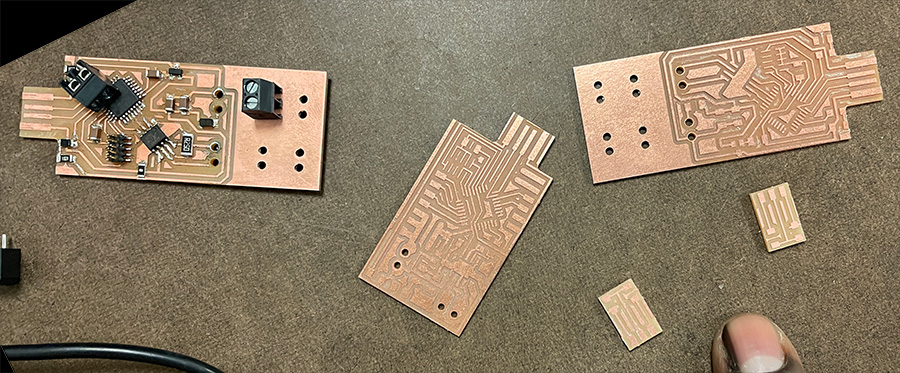
mill / stuff
milling the board
clean board
solder paste
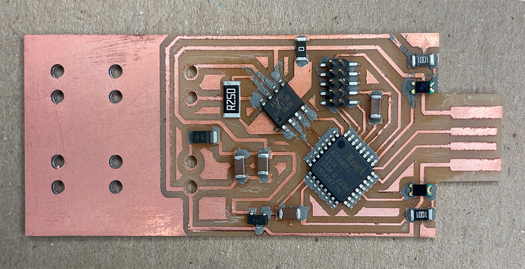
solder paste on board (too much)
reflowed
heating plate didn't work to reflow solder paste
my board got too toasty instead
tried to use solder paste on every component (not good idea)
so i touched each pin with the iron to reflow
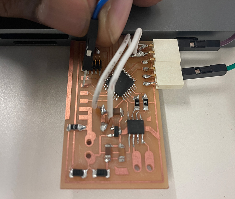
bootload
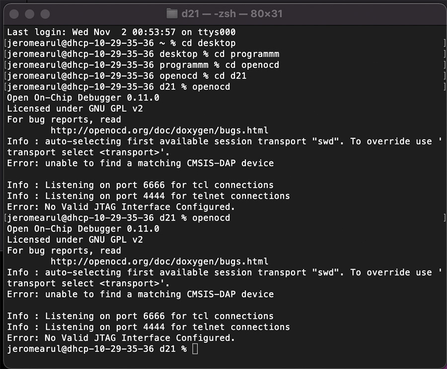
open ocd error : no jtag
no green light on ATMEL ICE
Error: unable to find a matching CMSIS-DAP device
Error: No Valid JTAG Interface Configured.
ugghh...
Assume there's no power to the board, or short somewhere
checking shorts with a multimeter, everything's connected !!
i.e 5v is connected to GND !
reviewing my schematic, phototransistor is also wired incorrectly.
there is no VCC line.(see below
back to breadboard
back to basics
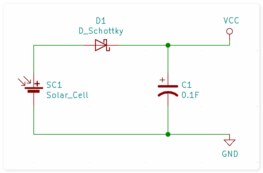
okay so plan b, let's just hook up this motor to a solar panel.
i have these 5.8V solar panels that were from a reject pile.
they work fine, the leads needed to be resoldered.
then wire in the diode (IN4007 instead of a schotty) and a capacitor.
on a breadboard.
source: bitbang
Ah is stored charge in battery
1 Ampere⋅hour = 1 Coulomb⋅hoursecond = 3600 Coulombs
Supercapacitor rated in Farads and Voltage
Ah= Farads*V/3600
= 1*5.5 / 3600
= 0.00152777777 Ah
= 1.53 mAh
Solar panel:
3.3 Wp 5.8V (imp: 567mA, isc: 613mA)
panel straight to motor
with capacitor and diode (not really)
resolved in week 10
pin out was wrong, need analog pins.
southside pins won't work:
pin 22 > PA23
pin 20 > PA19
pin-out northside:
pin 1 > PA00
pin 3 > PA02 - ANALOG
pin 5 > PA04 - ANALOG
pin 7 > PA06 - ANALOG
v1, v1.1, v2
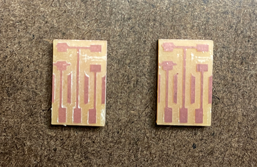
phototransistor breakouts
since i can't bootload both v1 and v2
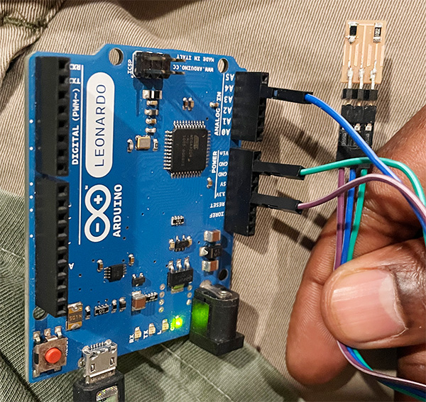
debug with leonardo
aren't burnt out
Leonardo: I can read voltage on the phototransistor breakout board,
but not through phototransistor
only use ANalog pins
phototransistor doesn't work, only resistor values
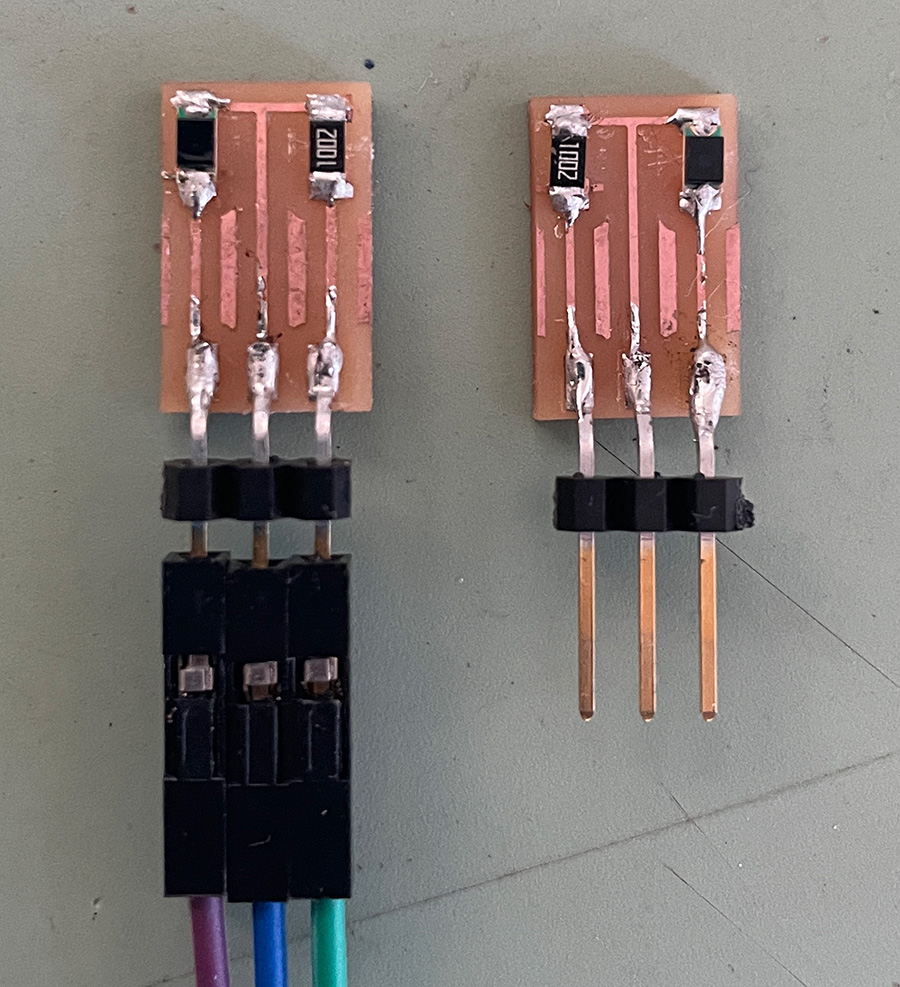
phototransistor breakouts
debugging with a Leonardo
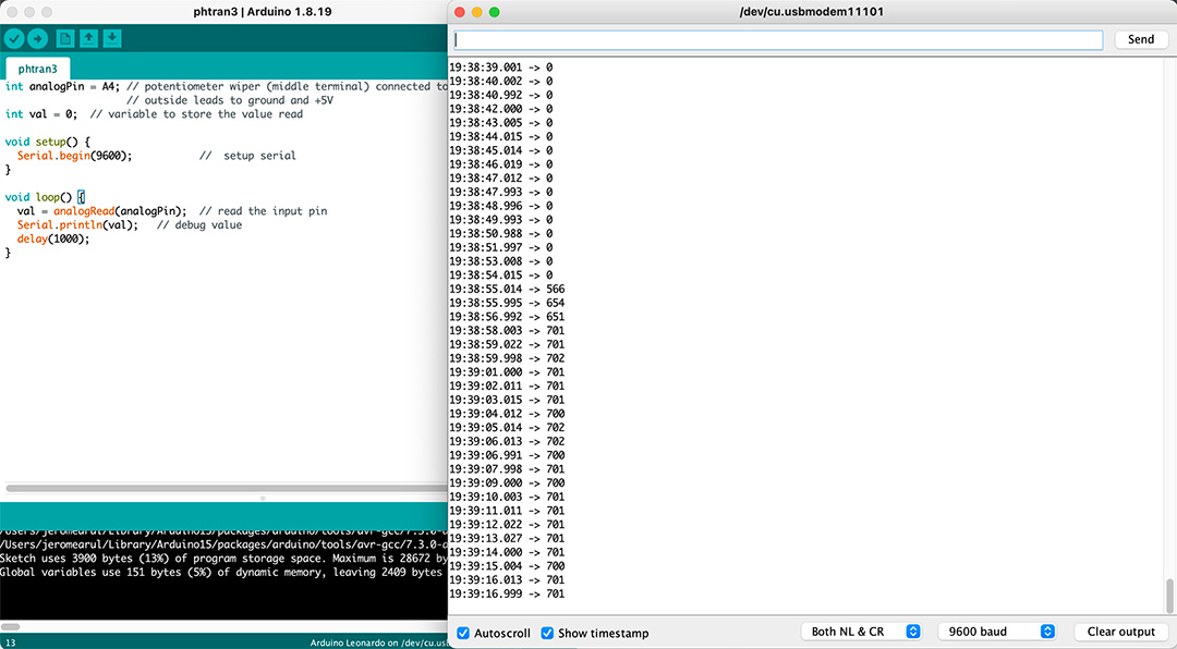
once bootload and serial print started working, it was easier to debug!
pinout to pin 2
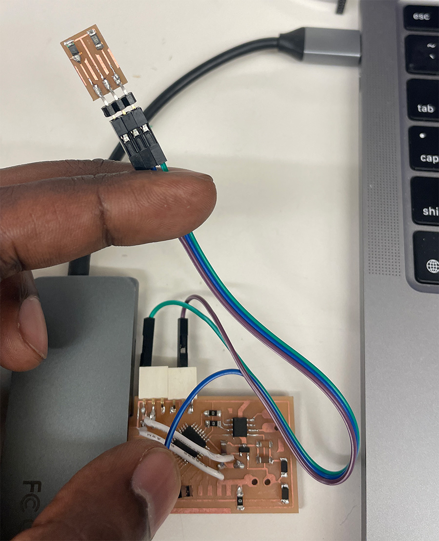
phototransistor breakout
had to use the northside pins
pin 2 was available and analog
also, flip the hot side and GND!
value is between 500 and 1024
resolution of ADC.
phototransistor test sketch
detects light!
check out week 10 for more on this board