Week 4,
Ideation Phase: The assignment for this week was to design a PCB. Naturally, I made the worst possible decision and started it at 1AM the morning of which it was due. I used Fusion360's electronics design software to first make my schematic which closely followed the hello-world board for the SAMD11C microcontroller, except our assignment included adding a button and a LED to the schematic. My schematic was so much messier than it should have been - complete with overlapping connections and not a single label - which I blame on my sleep-deprived state. If I were to do it again, I would incorporate labels and modules to make the schematic more readaable.
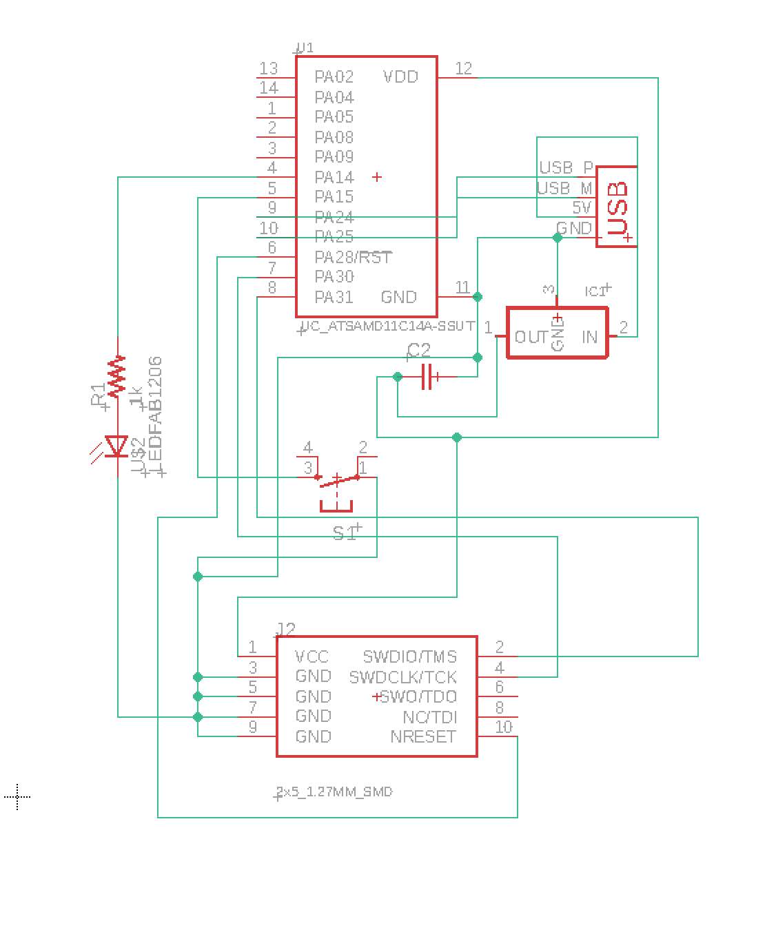
After that, I had to actually focus on the layout of the PCB. Basically, making the schematic creates 'airwires' between components that need to be connected together. After doing so, we still need to route the PCB itself and layout the components and draw the traces that will connect them all. This took quite a bit more time than I had originally intended. First of all, optimizing layout is like solving a puzzle except the puzzle takes place at 3AM in the Architecture shop while I remain unsure if I'm doing anything correct. Regardless, it ended up working out and I got to add some artistic flair by using rounded bends and fortunately, I didn't need to use any 0 ohm resistors which is a helpful trick to jump through a connection.
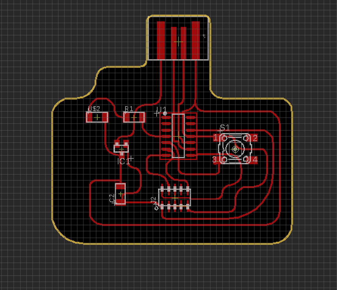
Execution Phase : As always, disaster struck (but luckily Anthony - shoutout to the EECS head TA - pointed it out) but my traces were too small. Instead of
the recommended 12mil, I had done 6mil traces. This wasn't a huge overhaul with the handy dandy 'change width 12' command by my side but it did mean I had to change my layout a bit to account for my necessary clearance and trace size. Once I'd done
that, I exported my PCB outline and trace layer as pngs (monochrome and 1000 dpi) and then edited my trace layer in Illustrator to add an octopus on a surfboard and a cute little phrase. In hindsight, I should have made them both bigger because on the
board, the images aren't really clear.
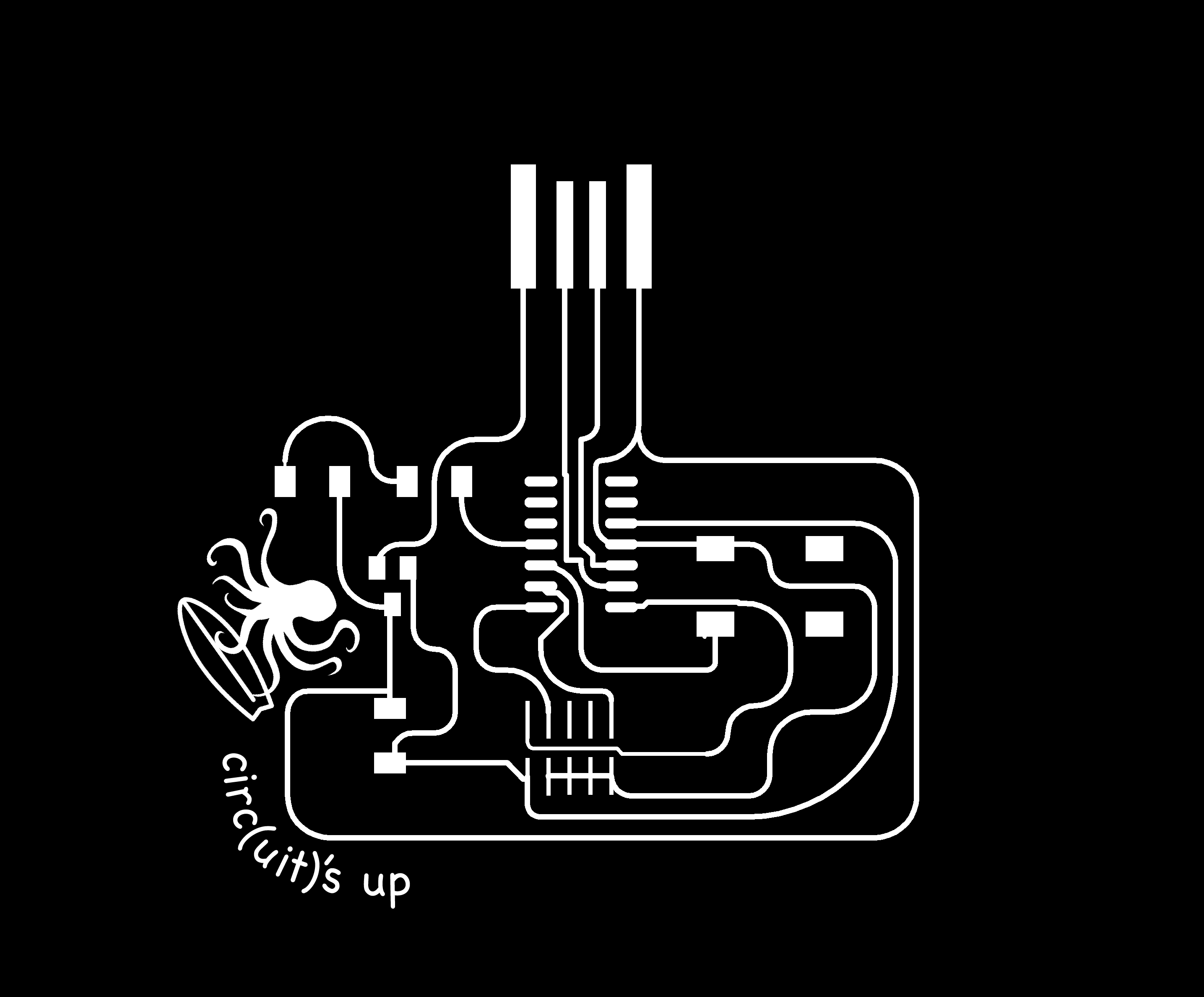
I hadn't used the Roland mill before and didn't realize how differently it operated. Instead of using gerber files, the Roland mill uses the pngs to make milling paths. I uploaded my pngs to the mill and analyzed the machine paths to see which
of my traces may end up being accidentally shorted or cut. Luckily, there were only a few iffy instances and those were corrected by modifying the expected mill size in the mods program to be a wee bit smaller.
Final Product:
This was my finished board:
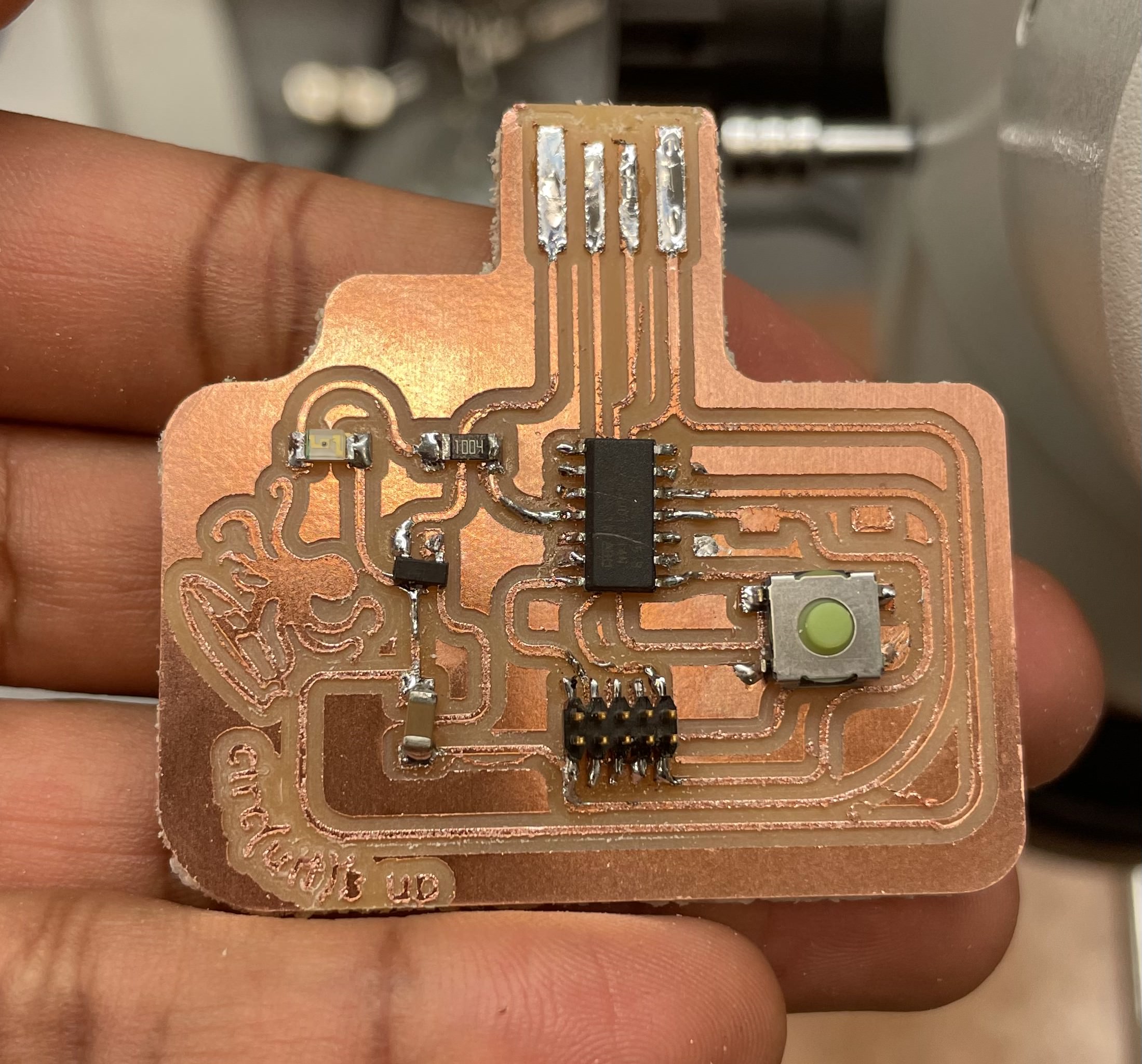
The board itself works and I tested it by uploading the 'hello board' program from the HTMAA website. Getting the board to a working state was no small feat. A few of the joints I'd soldered were simply not actually connected to the copper which
I found out through the use of a mutltimeter to test the connections between certain points on the board. Shoutout to the EECS team for our characterization of different testing
methods which ultimately came in handy. :)
- Alex