week 2: the pcb production pipeline
the CNC mill(s).
My section's lab space (EDS) has two mills: a Roland and an Othermill. These two mills function differently; the main difference is that the Othermill can't mill a board with a png file as input while the Roland can.
group assignment
This week's group assignment was to understand the design rules for the PCB production process. To do this, our section printed traces and cut spaces at varying widths. A png file was used for this linetest so we used the Roland to do the test. In the end, we discovered that starting from around 11 mil and lower, the integrity of the copper sheet begins to deteriorate.
The smallest space width that could be achieved was the width of the end mill (as expected). Additiionally, we found that in order to make efficient cuts, we could split milling between different end mills; generally utilizing the 1/32" end mill for thicker, batch cuts and the 1/64" for detail work.
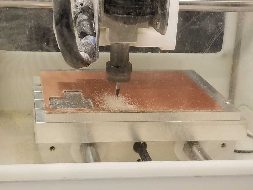
the milling process
Upon reccomendation by the lab TA, many of people in our section opted to use the Othermill over the Roland. The only issue with this choice was that the in-ciruit programmer circuit diagram provided for the assignment was given in png format, which the Othermill does not support :(
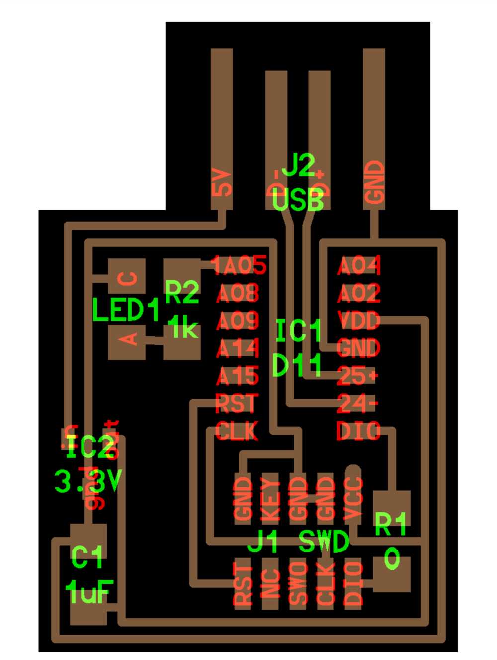
We talked about porting the design to svg or Gerber format, which the Othermill supports. Converting from png is tedious, and to maintain the size, correctness, and sharpness of the image, it would likely just have to be recreated. Our TA Anthony helped with this problem: he recreated the circuit in Gerber format and set it on the Othermill for use.
Anthony also changed the circuit design slightly: opting to separate a voltage regulator and capacitor in order to prevent a trace that leads to the capaitor from passing under the voltage regulator. The above pictures show the old design vs the new design.
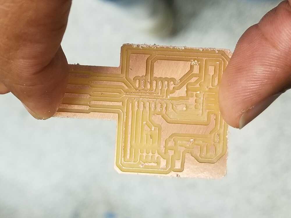
The milling process was completed in 2 parts: first with the 1/64 head for the detail work, and then the 1/32 head for separation and cutting the board out. This process took 11 minutes.
soldering
using a microscope to solder small parts changed my life
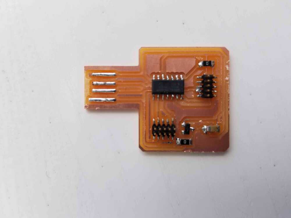
Next came soldering on the components (resistors, capacitor, voltage regulator, and swd chip). The eds lab has a microscope you can use so you can blow up the view of soldering process-- this made everything 200x easier. Anthony gave a good tip-- put some solder on the traces on the usb input for better contacts!
programming a programmer
make sure the edge of the usb is not shorted!
Before moving to programming, I had to be sure to scrape off the extra trace at the top of the design. This trace connected the usb traces, effectively shorting power to ground.
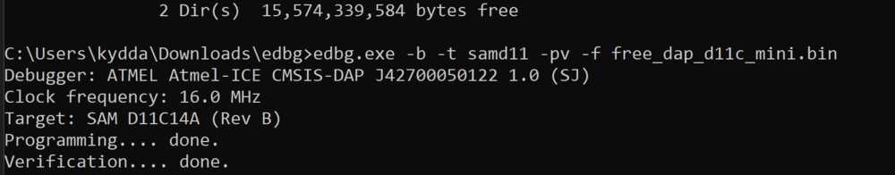
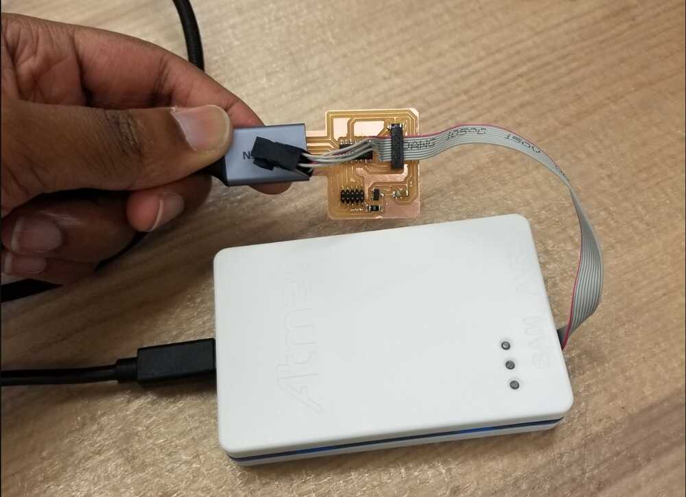
After scraping the copper off, I downloaded the programmer binary and used the Atmel programmer to send the program to my circuit. The above pictures show the program being loaded to my circuit. Whew.. worked the first time!
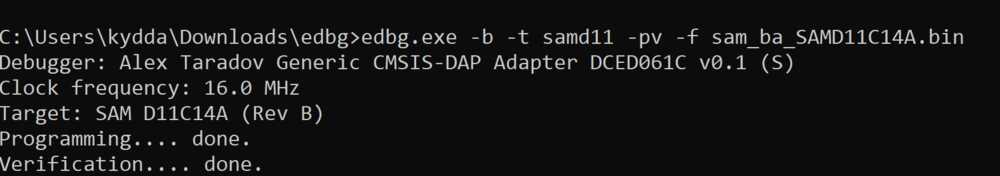
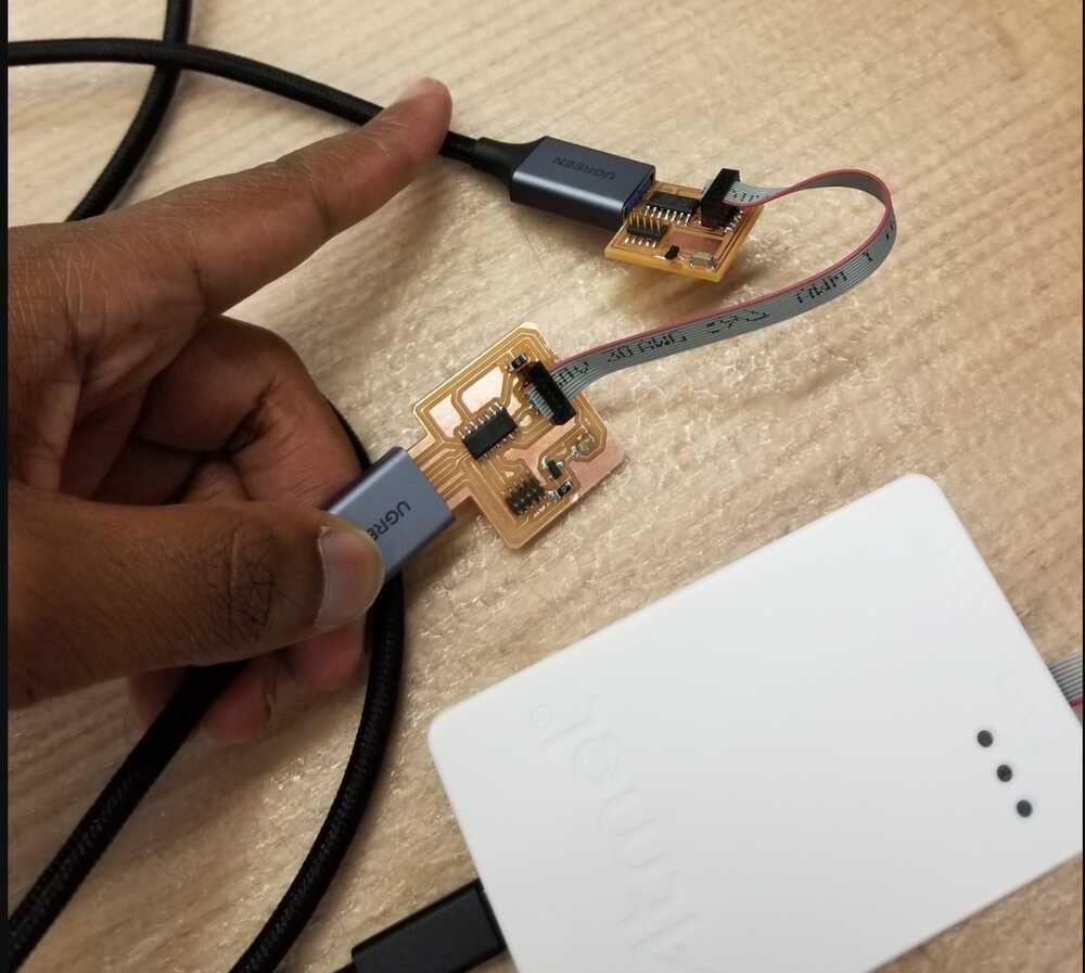
After this point, I used an example circuit for this assignment that was lying around and programmed it using my new programmer! The above pictures show my computer using my circuit to program another circuit.