Week 4: Electronics Production
Group Assignment
Group assignment answers can be found here: Group Assignments
PCB Design
This week, we had to design and then stuff a PCB that could then be programmed, and we had to verify that it was truly able to be programmed. At the minimum, we needed to add an LED (and the resistor that came along with it), as well as a button. After watching and reading through different tutorials, I started to design my PCB in Eagle (through Autodesk). I started off with the ATSAMD11C-echo board as a guide.
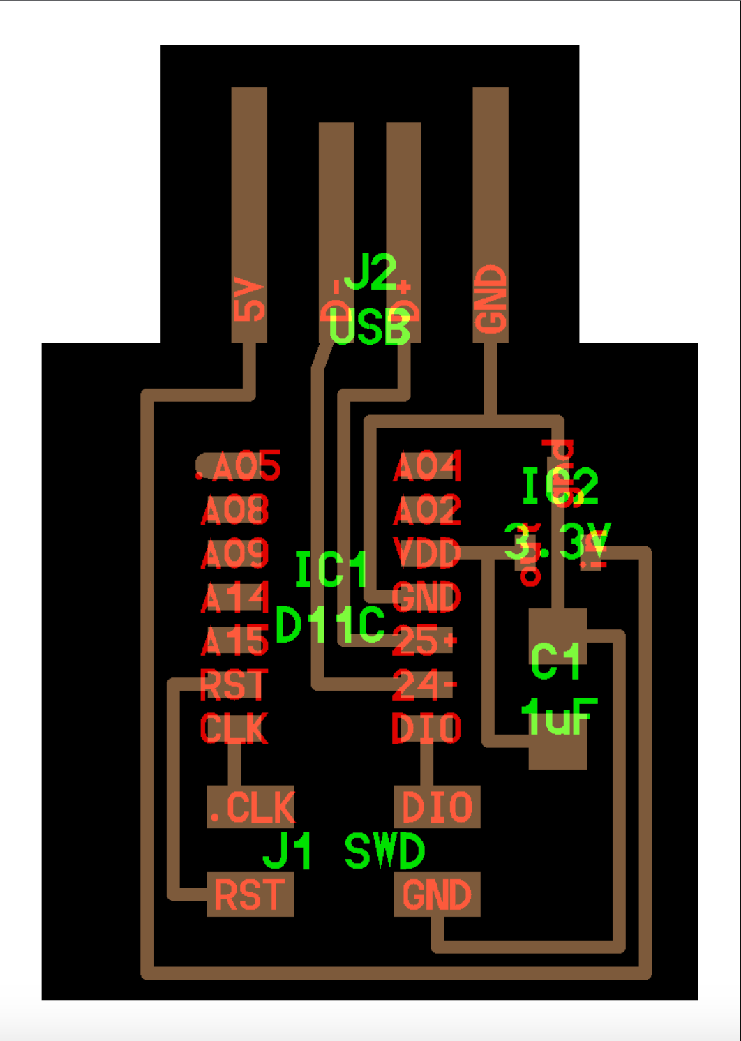
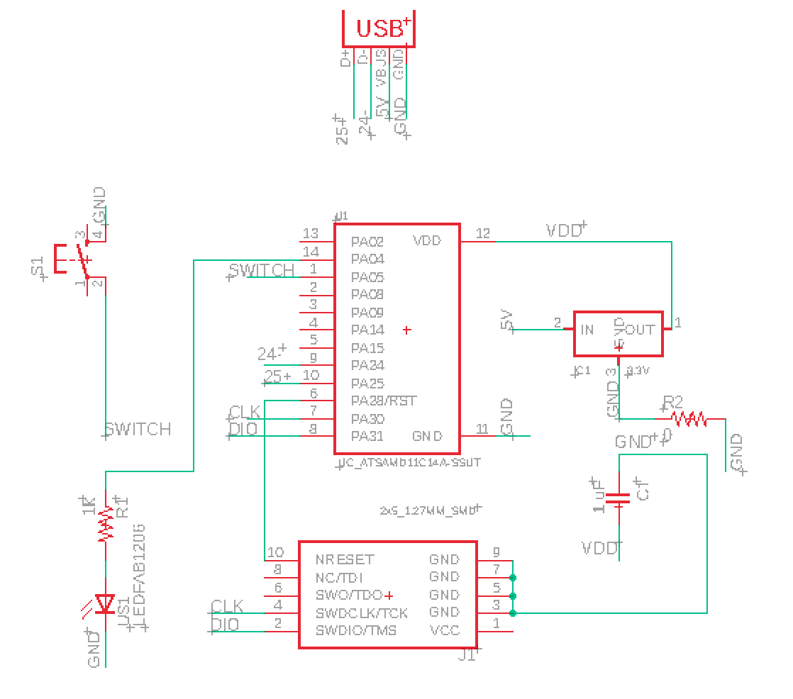
I placed the following parts down in my schematic: first, the ATSAMD11C microcontroller, 10-pin header, 1uF capacitor, USB port, and the 3.3V voltage regulator. Then, for the assignment, I added a button, a white LED, and a 10k resistor to go along with the LED. I made the necessary connections according to the template board. Then, for the parts I added, I made a connection between one side of the button to a pin on the microcontroller, another side of the button and ground, and then connections from the 10k resistor to a microcontroller pin that was analog or digital, a connection between the LED and the 10k resistor, and finally from the LED to ground. It took me a little figuring out to know where to connect the header pins to the microcontroller pins, but I figured out that there was a certain way of numbering the microcontroller pins (1-7 down the left side, then 8-14 up the right side). So I would just look at the template board and figure out what number the pin was on the microcontroller, and then make the connection to the pin with the correct corresponding number in my schematic. The SAMD11 datasheet also gave information on what type of pins they were. It was quite convenient to also have the naming function so I didn't have to have nets going everywhere.
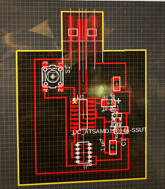
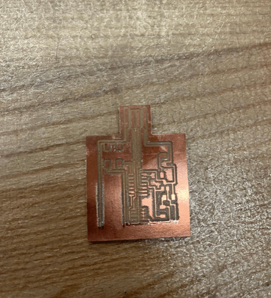
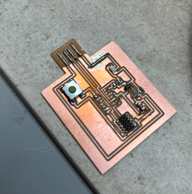
Once I finished my schematic, I started placing the parts on a board and attempting to arrange them to have the least crossovers. I started playing around with the routes, and went through lots of trial and error. I learned at this point to not use the mirror function, because that places the part on the back of the board (which I didn't realize until Anthony told me, I had thought it had just turned blue because the part was mirrored or something). I placed some parts following the template board, and then placed the additional pieces as I thought they worked best. I also learned that the closer some parts were to the center, the less likely there would be intersections of traces that would require a jumper (a 0 ohm resistor). While I was routing, I also learned about the convenience of being able to draw traces underneath some of the different parts. I had to go down to 8 mil for some of the traces that went underneath parts when there were multiple, but otherwise I used 12 mil for the trace width. As I was attempting to route, I realized I'd need to put one jumper in to get from the capacitor ground end to the voltage regulator ground end, so I went back to my schematic, put the 0 ohm resistor in and drew the appropriate connections, then placed it on my board. Once I drew out my board shape (making sure that the outline was snug along the USB port) my board design was complete!
I sent the board to milling, and waited for the board to be done.
PCB Milling, Stuffing and Testing
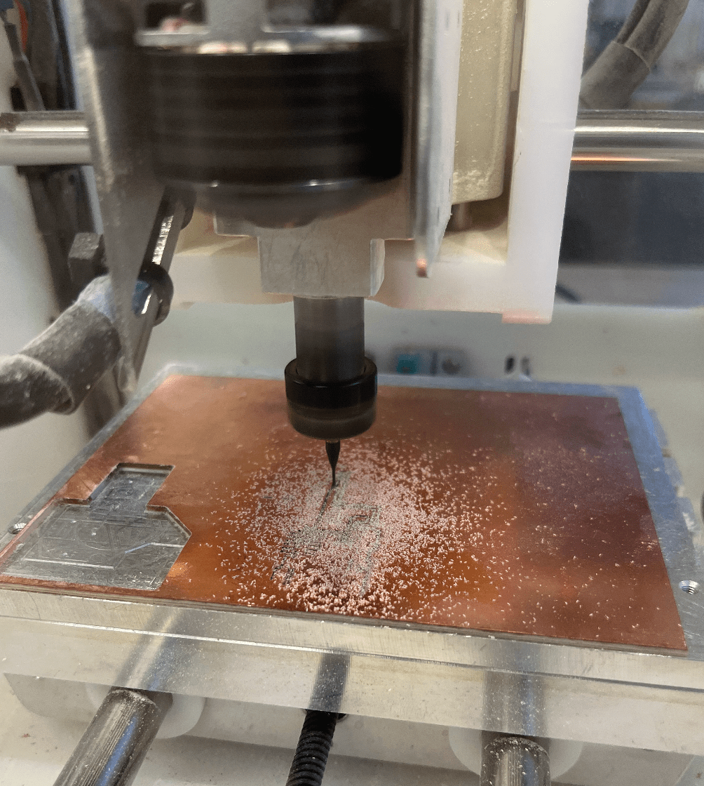
I changed the mill tip in the middle, then left for a bit. When I came back, the board seemed to be done milling, but when I looked at the board, the final traces at the bottom of the board were missing.
I found out that someone had taped the board down in an unideal way (the end of the board didn't have tape on it), so the bottom edge of the board had no tape. When the machine tried to mill the traces, the board bent down just enough that the mill tip was no longer in contact with the board. So, sadly, I had to re-mill my board, this time positioning the board a little higher up so I wouldn't run into the same problem again, since the entire board was already taped down into the PCB mill. I learned that a better way to tape the board was to use three-ish pieces, two for two edges and one in the middle. This would make it harder for a board to bend down like that, because it would be constrained on two ends rather than one. Anyways, my board got successfully milled the second time.
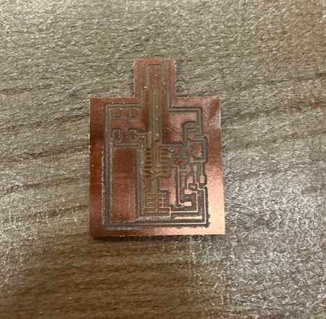
I proceeded to stuff the board with the correct parts. It was much easier this time than last time, because I had used a thicker mill tip when I could, so there was more space between the traces. It was then time to try to program the board and test it.
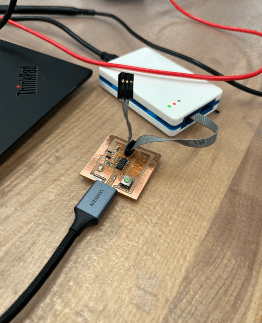
The first problem I ran into was that the board was shorted, and we found out it was because there was a small piece of copper that hadn't been milled away by the machine when it should have. However, that didn't fix the problem. The next thing I realized was that my board was missing a connection. I had went off of a board design with a 4-pin header, not realizing that a 10-pin header would have extra connections. So, I fixed this by taking a thin wire and making the appropriate connection from the header. However, it still didn't work after that. One connection that should have been made wasn't there. It had a trace going underneath the microcontroller, so I took the microcontroller off using the hot-air soldering machine and realized that part of the trace had been scraped off somehow, so it was missing. I wasn't sure when this had happened, whether it was during the milling and I just didn't notice when the board came out, or if it happened when I was soldering the parts down.
I tried first to fix this by putting a small wire along the trace. This did fix the connection, but when I tried putting the microcontroller back down, it was too uneven and I would have needed to bridge an air gap with solder to put the microcontroller back in. So, instead, I took the wire back off, put the microcontroller back on, and then connected another external wire. So now, my board had 2 external wires.
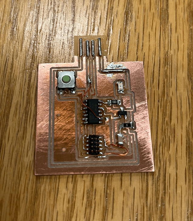
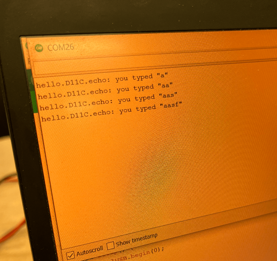
However, after this, all the problems were finally fixed, and my board was successfully programmed to echo!