PCB Design, Milling, and Soldering
PCB Design
This week we learned how to design PCB’s and fabricate them using a PCB mill. We learned that electronic products are first designed as a schematic diagram showing the connections between parts, then translated into a PCB using circuit design. Various software exists to do this: there’s Altium, which I’m familiar with, as well as Eagle and KiCad, which are free software that Neil suggested.
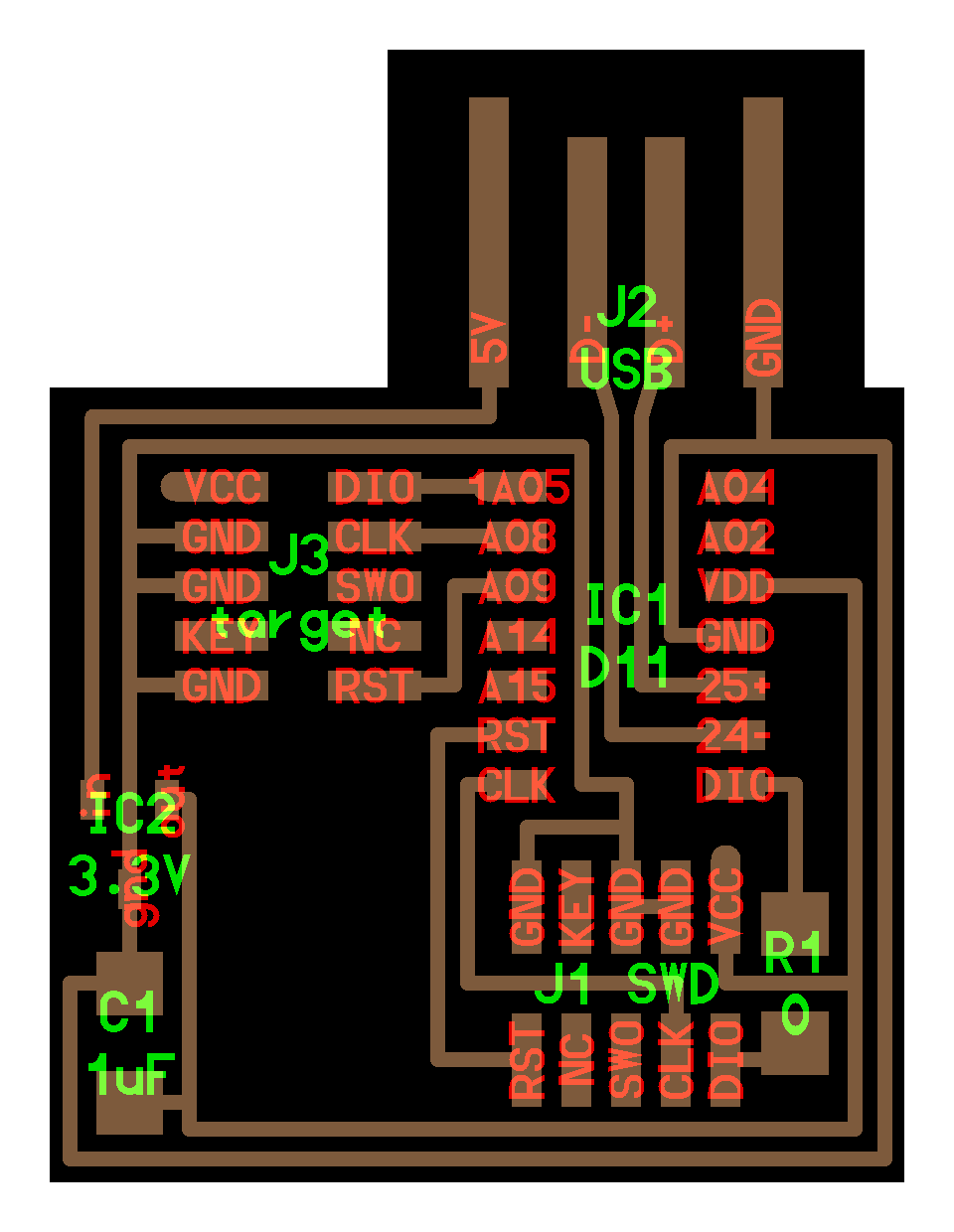
We were making a programming board for programming microcontrollers, so we pulled some existing PCB files from the class website. The files themselves were Gerber files, or a set of files describing each layer of the circuit board. Gerbers, despite being a very old standard, are the industry standard in PCB layout files. Another alternative explored in the class was using black and white PNG images to mark where to keep/remove copper from the circuit board; this is not common and the class uses custom software to do this.
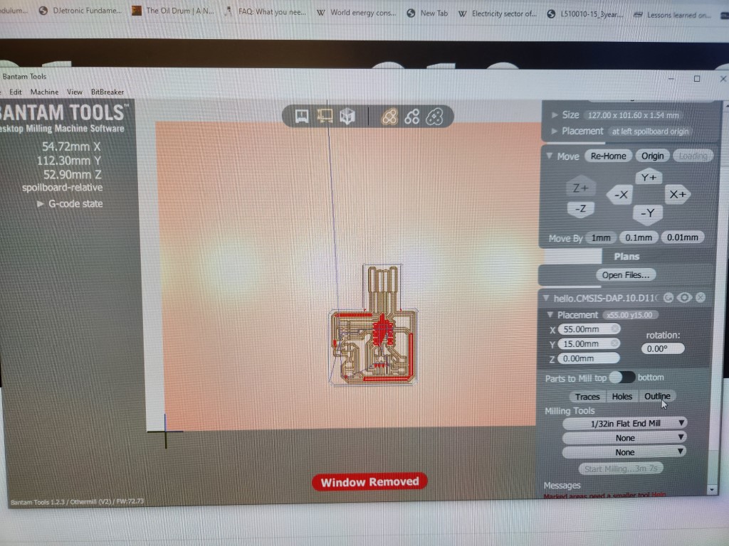
We loaded the Gerber files into Bantam Tools software. Momentarily, a rendering of our circuit board popped up in the software.
PCB Manufacturing
Before cutting the board, a group assignment was to characterize the PCB mill, particularly how small it could cut. The group cut a test board with traces of decreasing sizes; the conclusion was that minimum trace width is 10 mils. Link here.
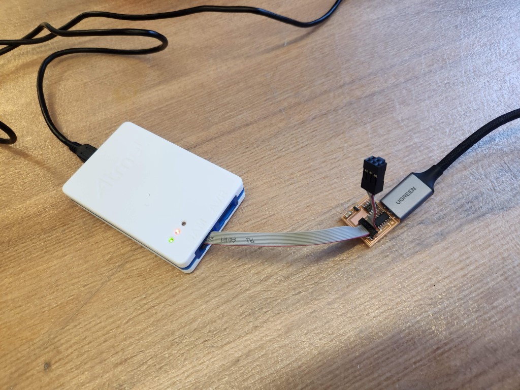
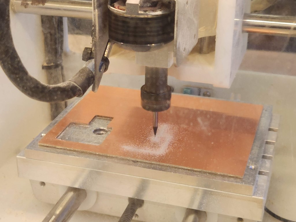
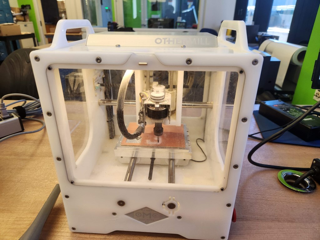
We used the Othermill PCB mill to make our boards. We loaded in a fresh sheet of FR-1 PCB material, swapped the endmill for the precise 1/64” tool, then hit play. The mill cut away the traces of the PCB smoothly.
We then swapped endmills for a larger 1/32” endmill to cut the outline of the board. With the board milled, we pried it from the sheet of FR-1.
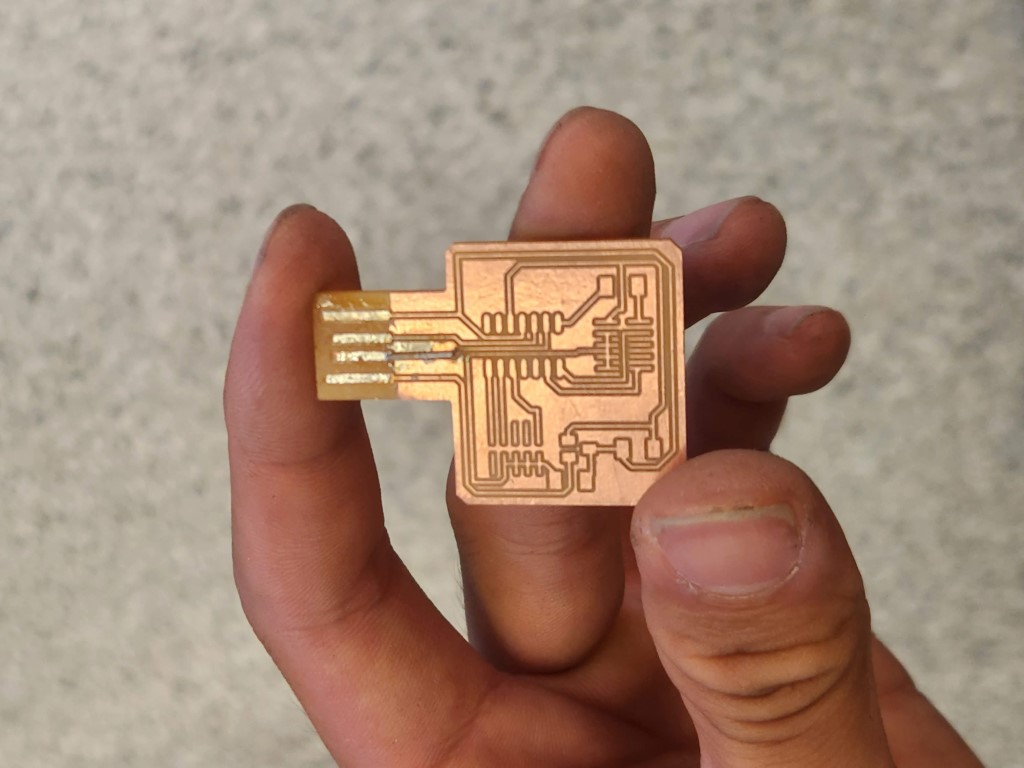
One issue is that the USB connector built into the design had a lot of copper surrounding it, which would cause a short circuit when plugged into the computer. We had to manually remove the copper around the USB connector using X-Acto knife, but I don’t see why we couldn’t have removed the copper inside the mill instead.
I sliced one of the USB connector wires by accident while removing the copper, so had to improvise a fix. I soldered a wire bridging the connection, which took some finessing. Electrically, the circuit was repaired.
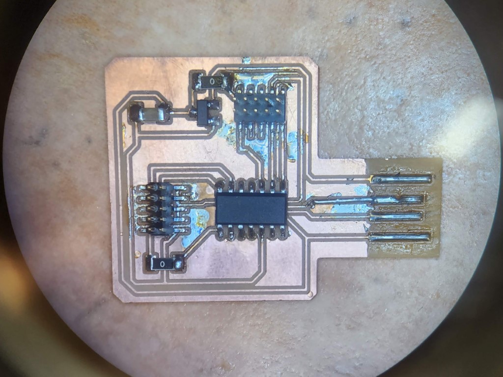
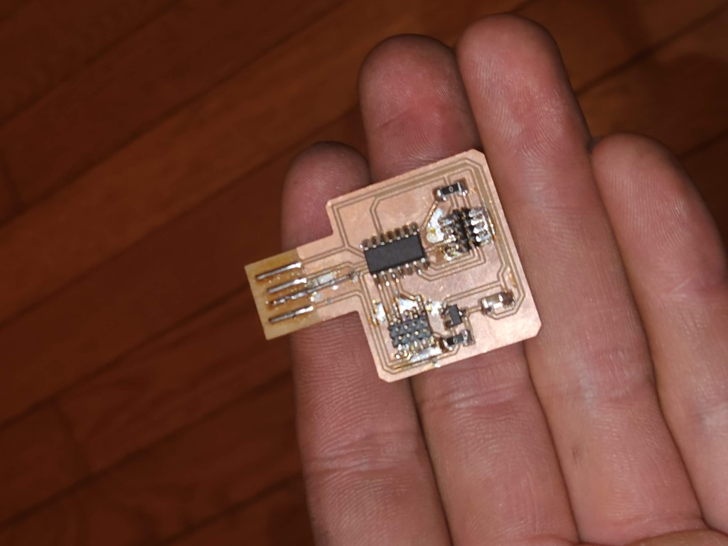
Then I populated the board with components. The components were all surface mount, meaning they sit on top of the board and are also soldered on the same layer. The components of this board included the microcontroller, a connector to the programming target, a connector to program the microcontroller itself, a voltage regulator, and a filter capacitor. There were also two 0-ohm resistors on the board acting as jumpers to help with layout.
PCB Testing
With a completed board, the next step was to upload the firmware to turn this board into a programmer. We used a pre-written firmware and the EDBG programming utility to program the board through an Atmel programmer. We used the command:
The board successfully programmed, and I was able to use my board to program another board!