Week 6 - Embedded Programming
This weeks assignments covered programming of the boards built in Week 4. Since I had several issues in getting my computer to recognize my board, this week's assignment took a little longer than anticipated and also included milling and stuffing several other boards. Luckily, I anticipated some setbacks and only targeted designing a simple board with a button and LED, such that the button turns the LED on through software. I figured once I can get that to work, more complex setups are simple and can be left to the final project.
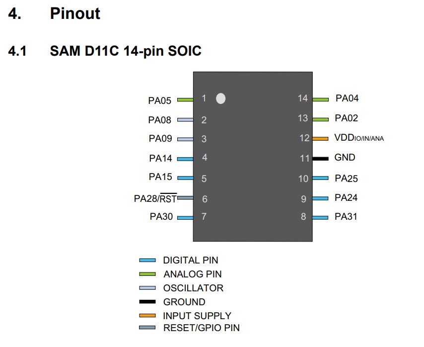
The first thing to note before design the board is the pin layout of the selected microcontroller, the SAMD11C14A. This pin layout can be found in the datasheet of the device. A reference design for the bootloader board was used to for the pin header connections to the microcontroller in order to make it programmable via USB. The pin layout from the datasheet is shown below.
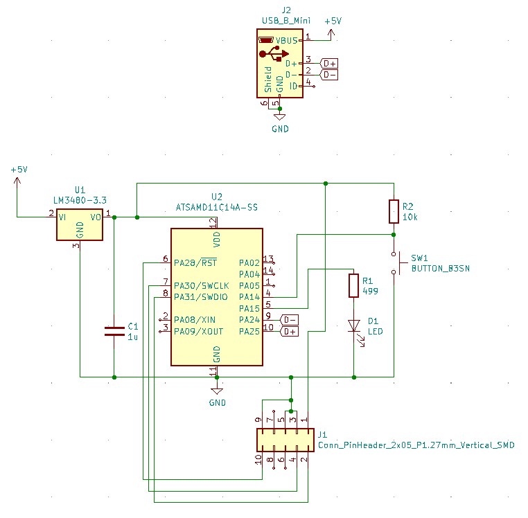
With this pin layout in mind, the schematic for the board layout, a simple button and LED setup, was generated. Pins 9 and 10 (PA24 and PA25) are designated as the data lines to and from the USB. For integrating the button and LED, two of the available digital pins are used, one for each component. Pin 5 (PA15) is an available digital pin used to output to the LED. A resistor of 499 Ohms is used as a current limiter in series with the LED. Pin 4 (PA14) is an available is an available pin used to read the voltage from the button. One end of the button is connected to ground and one end of the button is connecting the digital pin on the microcontroller. However, that pin must also be connected via a high resistor to VCC. The large resistance means that no current flows and no voltage drops across the resistor, essentially tying the pin potential to VCC instead of having it float when the button is not pressed. When the button is pressed, the voltage at the pin is ground. The circuit schamatic in KiCad is shown below.
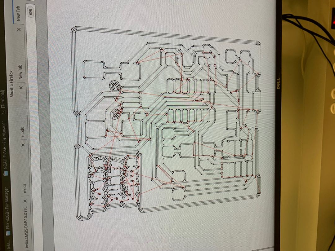
The board was exported as a SVG in two layers. The first is the copper layers and the second is the outline. This SVG was imported into mods' SVG to PCB program and the traces were generated, shown below, before sending the file to the Roland mill in the EDS shop.
The result of the board milling was strange as can be seen below. The edges were cut to close.
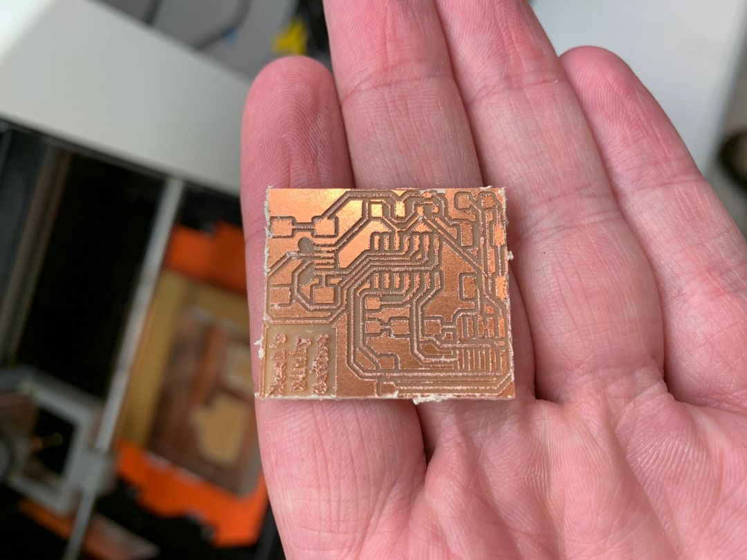
Upon further investigation I found that the board loutline was cut on both sides since it was not a copper fill, it was just a line.
Regardless, everything seemed to be electrically intact, so I proceeded with stuffing the board.
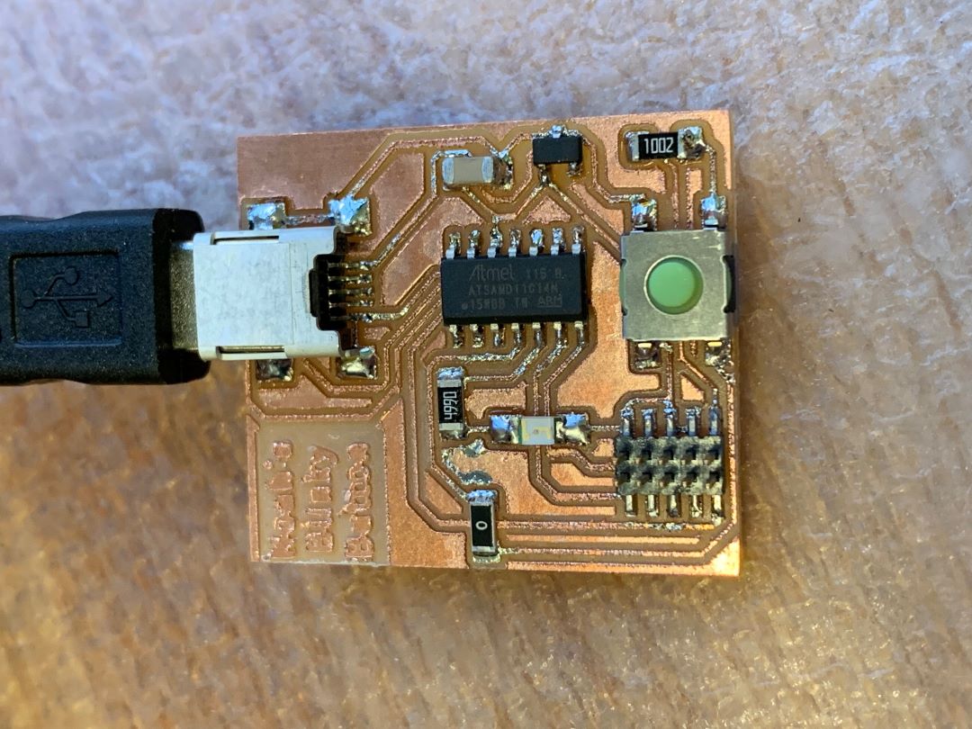
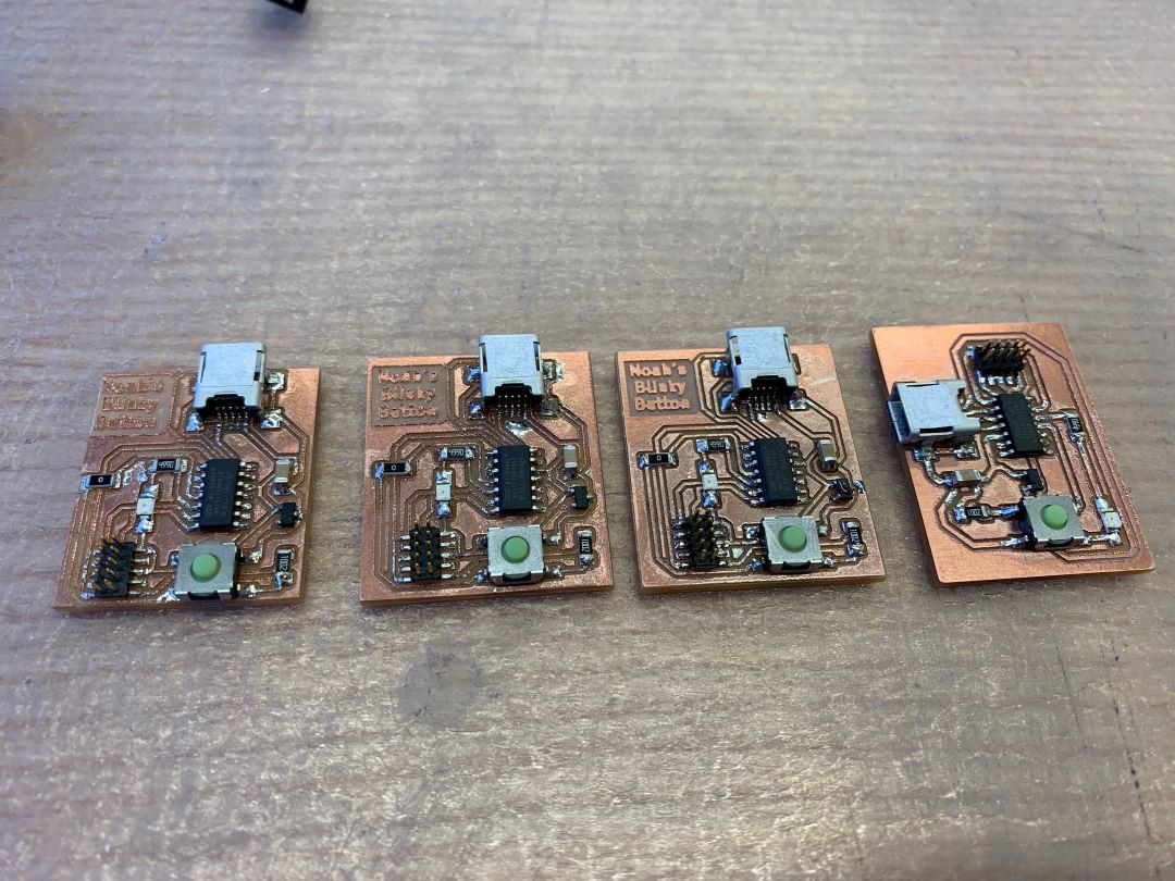
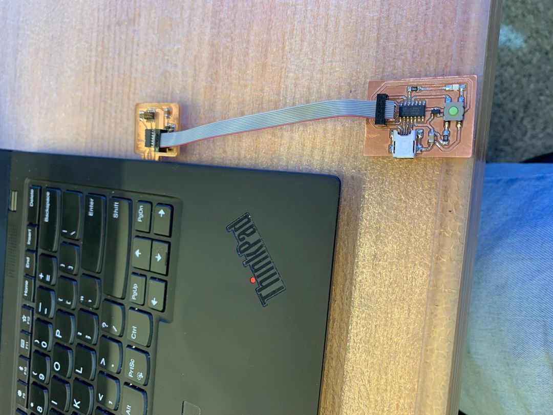
It turns out the board didn't work for several reasons (as I will go into later). I ended up making a total of 4 boards for this weeks assignment in order to debug what was wrong. The first reason the first board didn't work is because the data lines, which travel underneath the mini USB connector, were shorted together. This is because the outer casing of the mini USB connector is at ground potential and the traces are directly in contact with the case when they travel underneath it. I used the mini USB connector instead of the USB connector because I didn't have the footprint for the USB traces. So I eventually figure this out and made a second board. This time I placed electrical tape (in the future I would use Kapton tape) underneath the mini USB connector. This board (supposedly) loaded the bootloader successfully, but my computer didn't recognize the microcontroller. So I made a third board thinking I must've shorted something while soldering (even though I double checked continuity). This board I built in the same fashion, but I actually did short something while soldering (underneath some component), so the third board didn't work. Finally, I redid the PCB and trace layout such that there were no more traces underneath the mini USB, larger traces for milling reasons, fewer traces under components (and opportunitites to short something out), and 0 Ohm resistor jumper. This board worked in the end, but no initially. I suspect the 2nd board would also work.
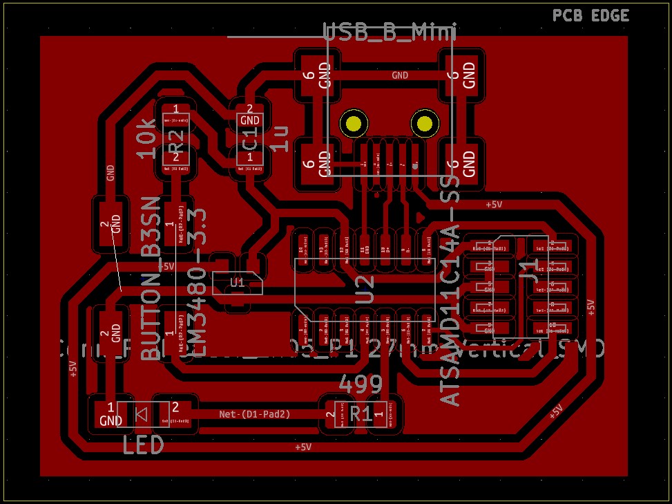
Final PCB layout.
So why didn't the two boards work immediately. For a couple reasons: some are my fault, and some are the result of misleading verbose software. The first reason is that I did not initially provide power to the board via USB during bootloading (see below). I thought that the 3.3 V and GND from the bootloader board were transferred through the header to the board that's being bootloaded. This means that the microcontroller was not being powered during bootloading and couldn't have successfully been bootloaded.
However! The edbg and binary file that I was using printed out that the bootloading was successful, even though it wasn't. Further misleading me.
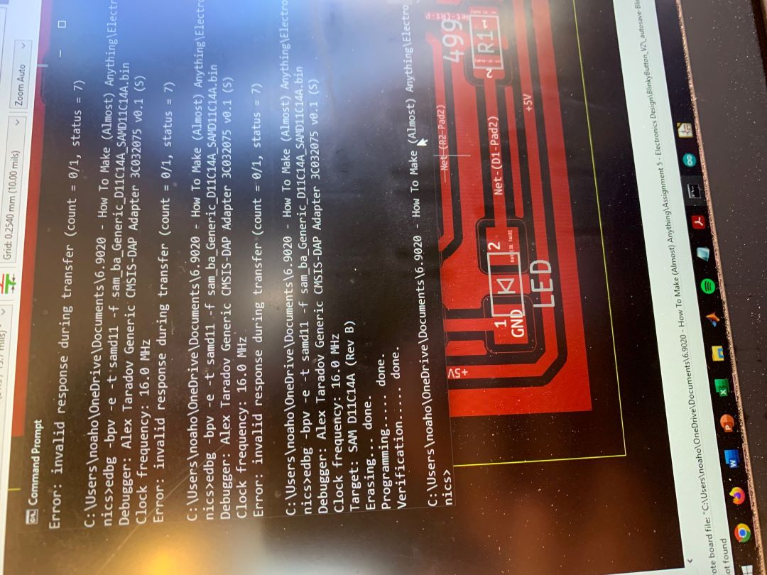
This confused me however, because when I went to plug in the board and program it through Arduino, my computer didn't recognize the board.<\p>
After I fixed the power problem by plugging in the USB during bootloading, I still had the problem that my computer didn't recognize the board. Finally, with the help of Anthony, we figured out that the binary file that I was using and found on a fab academy website was totally different from the one found at https://github.com/qbolsee/ArduinoCore-fab-sam/blob/master/bootloaders/zero/binaries/sam_ba_SAMD11C14A.bin. I downloaded this one and ran the following command in Windows' command prompt: edbg -b -t samd11 -pv -f sam_ba_SAMD11C14A.bin. After doing this, my computer and Arduino successfully recognized the board.<\p>
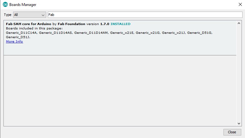
Next, to program the board using Arduino, the board manager needs to updated to recognize the SAMD11C14A. I used the following link to update the board manager.
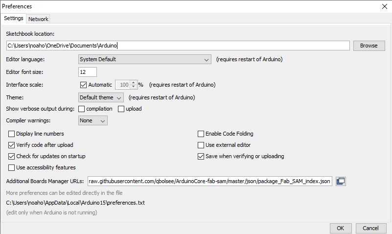
I then went to the board manager and found the microcontroller list that I wanted and installed it.
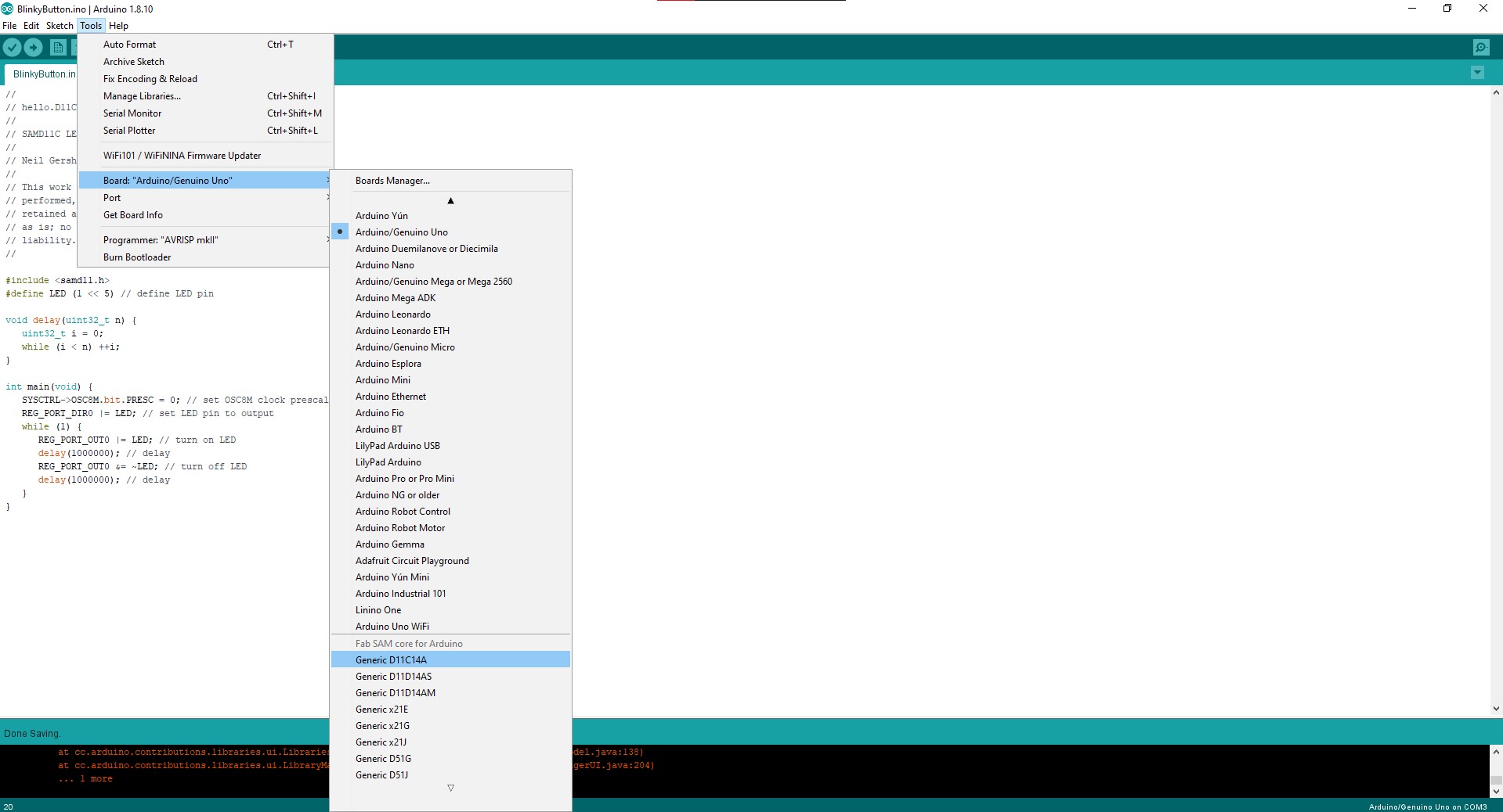
I then set the board to Genertic D11C14A.
Next I wrote up a simple program that reads in the button digital potential and outputs the LED. I have some experience programming in Arduino, so this was fairly straightforward and actually worked on the first try, however, the tricky thing to get right is the beginning definitions and counteracting the bouncing affect in the software. The button and LED pin numbers need to be defined and the pin mapping set to standard so that arduino know I'm using the PA numbering system to correlate physical pins. The two pins need to be set to input and output respectively in the setup. In order to counteract the bouncing, a timer is set to wait for the next press after some time to alow the button to settle. Each button press should toggle the LED.
#define BTN 14
#define LED 15
#define PIN_MAP_STANDARD
int start = millis();
int curr;

void setup(){
	SerialUSB.begin(9600);
	pinMode(BTN,INPUT);
	pinMode(LED,OUTPUT);
}

void loop(){
	curr = millis();
	int BTNStatus = digitalRead(BTN);
	if((BTNStatus==0)&&(curr>(start+20))){
		digitalWrite(LED,HIGH);
		start = millis();
	}
	else if((curr<=(start+20))){
		digitalWrite(LED,HIGH);
	}
	else{
		digitalWrite(LED,LOW);
	}
}
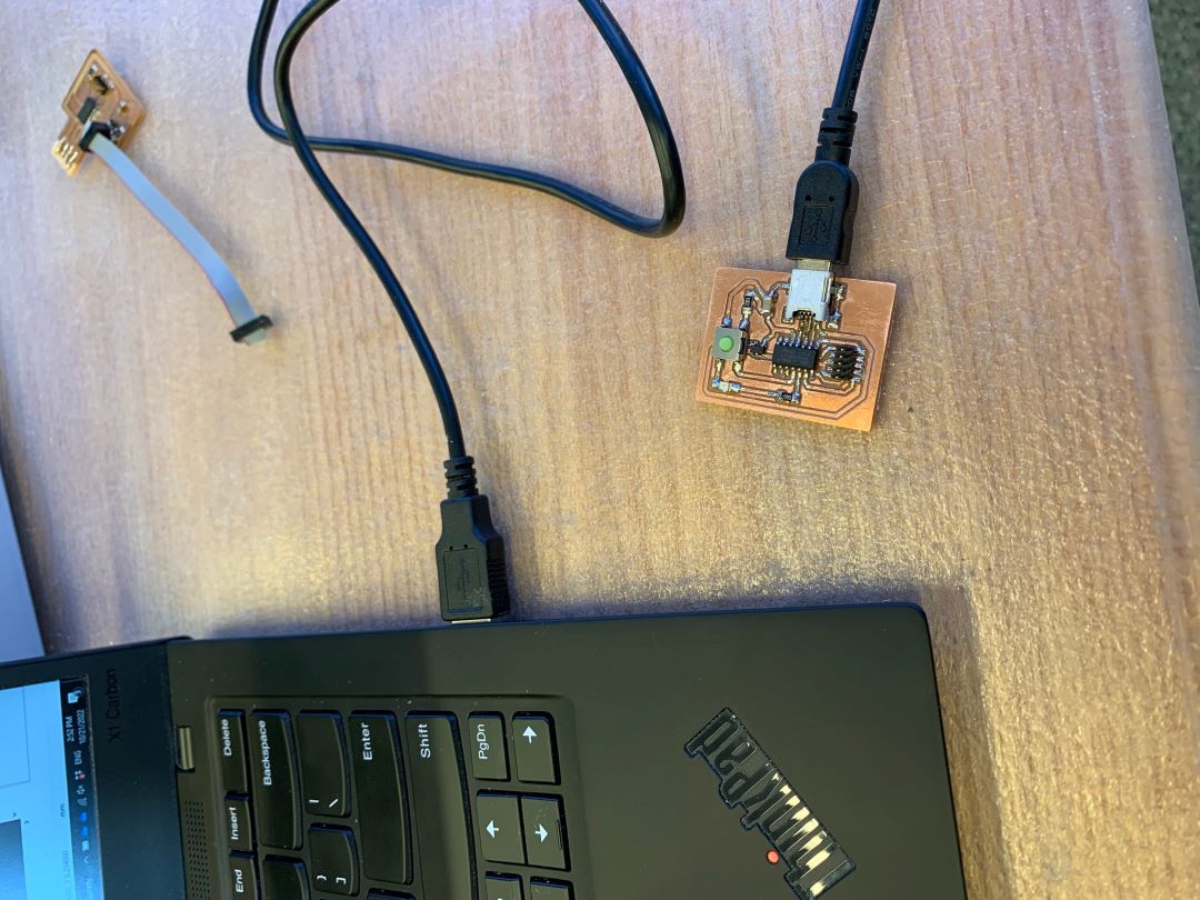
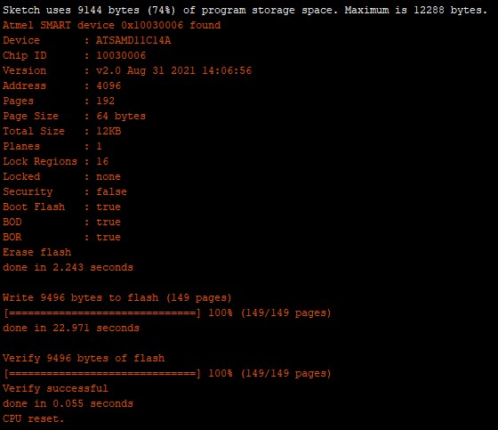
The program was loaded to the board successfully....
And here it is working on the first try!
Design files for this week can be found here.