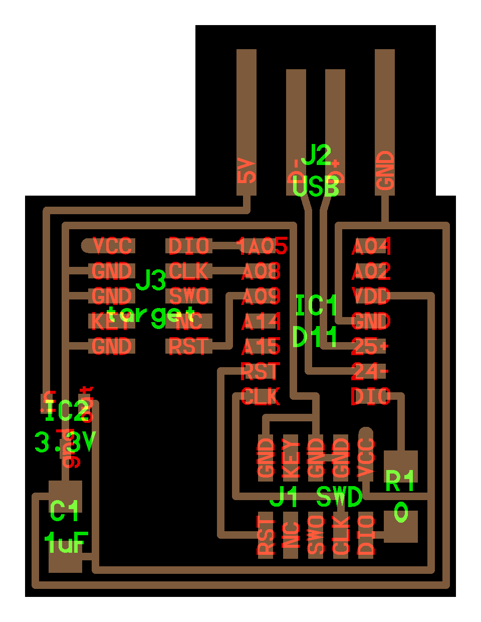
If last week was utilizing my little knowledge in CAD software to design and laser cut my puzzle cube, this week was much more challenging in that I didn't even know what PCB was or did. Still, through this week's project, I am proud to announce that I have successfully built my first PCB! The PCB contains one 1 uF capacitor, two 0 ohm resistors, a USB port, two connectors (J3: a target for the device I'm programming & J1: to program the chip itself), and one microcontroller.
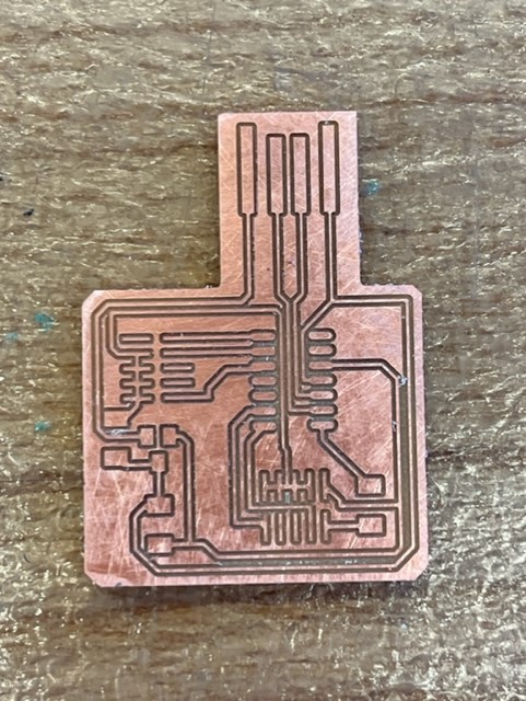
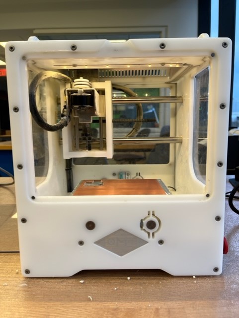
I printed the circuit using the given design. I first taped the PCB onto the milling machine and adjusted the xyz coordinates to initiate the PCB fabrication using OtherMill. During the machining process, 1/64" bit was used to mill the circuit traces, and 1/32" bit was used to mill the PCB outline. Then, I cleaned dust using a vacuum cleaner and removed the board from the plateform using a screwdriver. Finally, I filed the surface to smoothen the etched copper. The board looked great without any damage to the circuit!
When I first heard about soldering in class, I was intrigued by the idea of melting lead to connect different circuit components.
When it was my time to solder, I was surprised by how small and delicate each piece was, particularly the resistors and the capacitor.
Therefore, I used a microscope for easier visibility.
1. I applied flux on the regions of interest (where soldering will occur).
2. I gently placed the heated solder (750F) near the component on the printed board.
3. Bringing lead wire close to the tip of the solder, I melted the lead and soldered the component onto the board.
4. Repeating this process, I completed making PCB. Throughout the process, I accidentally dropped the lead so using the solder wick, I cleaned the surface.
5. To enhance the USB connection, I removed the copper near the port using an Exacto knife.
*Additional note: The flux serves as the wetting agent that helps uniformly spread the lead & The flux also removes oxidation and prevents airflow to the lead, preventing further oxidation (wouldn't want rust/corrosion to damage the PCB!)
First Failure :( |
Second Failure :( |
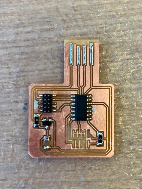
My Success! |
I accidentally switched the orientation of the microcontroller, which was unfortunate. I attempted to remove the piece (with the help of Dave in the EBS lab) but ended up deciding to make a new PCB. Nonetheless, I was very proud of my very first PCB (pretty good for a newbie)! 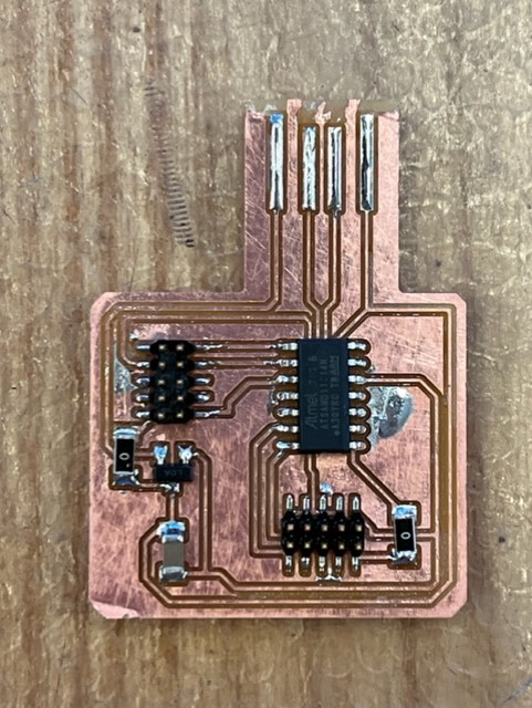
|
I thought I successfully made my 2nd PCB. All components were soldered in the right orientation and location. During the testing, I used the EDBG software to program the microcontroller (the programmer). The programming was successful, but when I removed the Atmel-ICE, a type of CMSIS-DAP device that can write programs into the microcontroller, J1 SWD (Serial Wire Debug) was also removed, indicating cold solder joint. I must have not properly heated the copper along with lead, leading to improper joints between the SWD component and the board. As shown in the picture below, copper remains. Nonetheless, according to Anthony (EECS section instructor), I was very lucky because SWD was disengaged after the programming was successful (I guess I'm a pretty lucky person)! 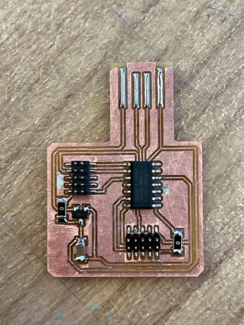
|
While it was temporarily fine for me to use my 2nd PCB, I wanted to give a final try and remake the board. I soldered thoroughly to ensure joints were connected and the result was awesome! After completing the board, I again tested/ programmed it using the EDBG software and my PCB device is now fully functional :) 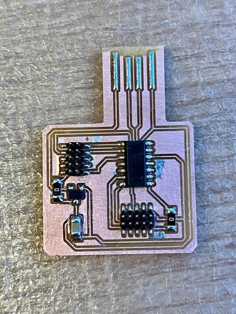
|
|---|
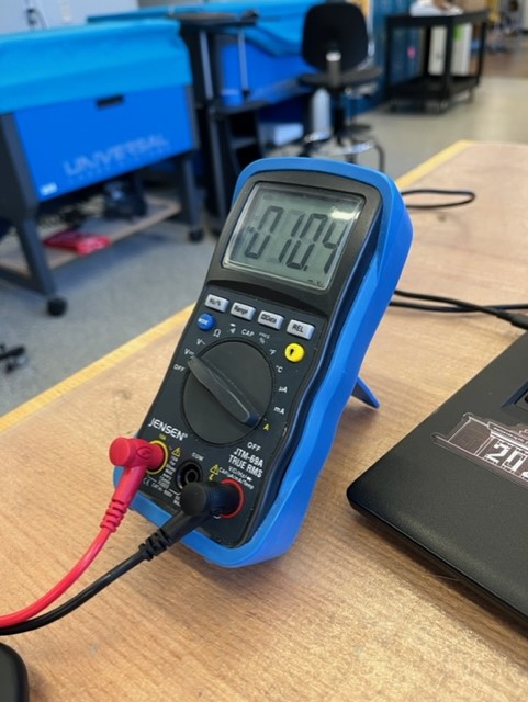
Again, using the process described above to confirm my PCB functionality, I confirmed that it successfully connected to my laptop. However, during the Jensen multimeter test, I found out that the clock was connected to the ground using "continuity test mode" (test to confirm if wrong connections are made on the board). While programming PCB worked successfully because it wasn't relevant to this week, this would be an issue in the future weeks when I'm using the target connect to program other devices. Therefore, I used an air-heating reflow machine to heat the particular piece and gently moved it to the correct position.