Week 04 - Electronics Design
1.1 Group Assignment
1.2 Individual Assignment
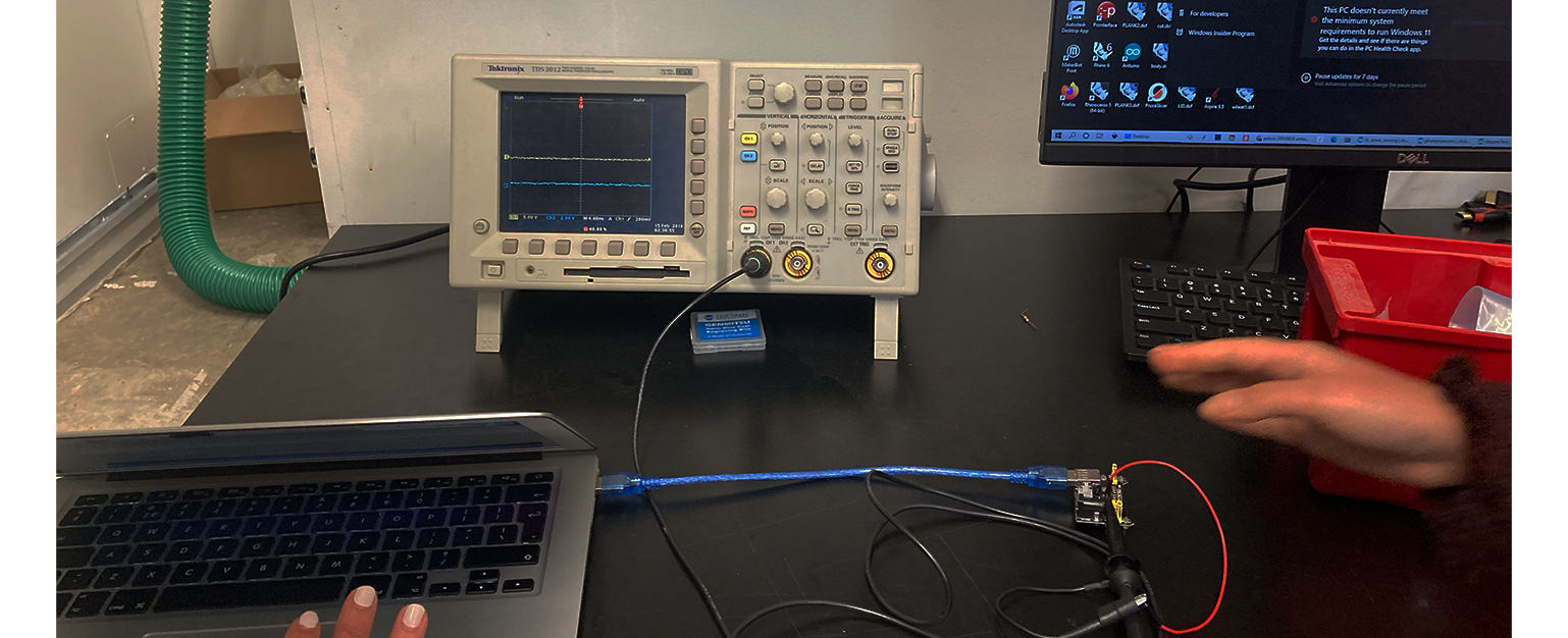
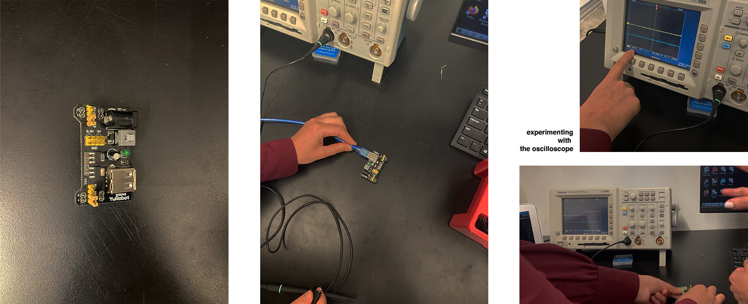
This week's group assignment was to use the test equipment in our lab, the oscilloscope to observe the operation of microcontroller circuit boards. After Leo introducing us how it works, we went ahaed and tried experimenting with it as a group. We picked up a board we found in the lab and wired it up to the oscilloscope. In order to observe the voltage fluctuations, the wire connection had to be between the ground and Power (5V in our case).
We were able to see how the operation signals as we turned the button on and off, which was very informative and interesting in understanding how the power visually behaved in cirtuit boards.
1.2 Individual Assignment
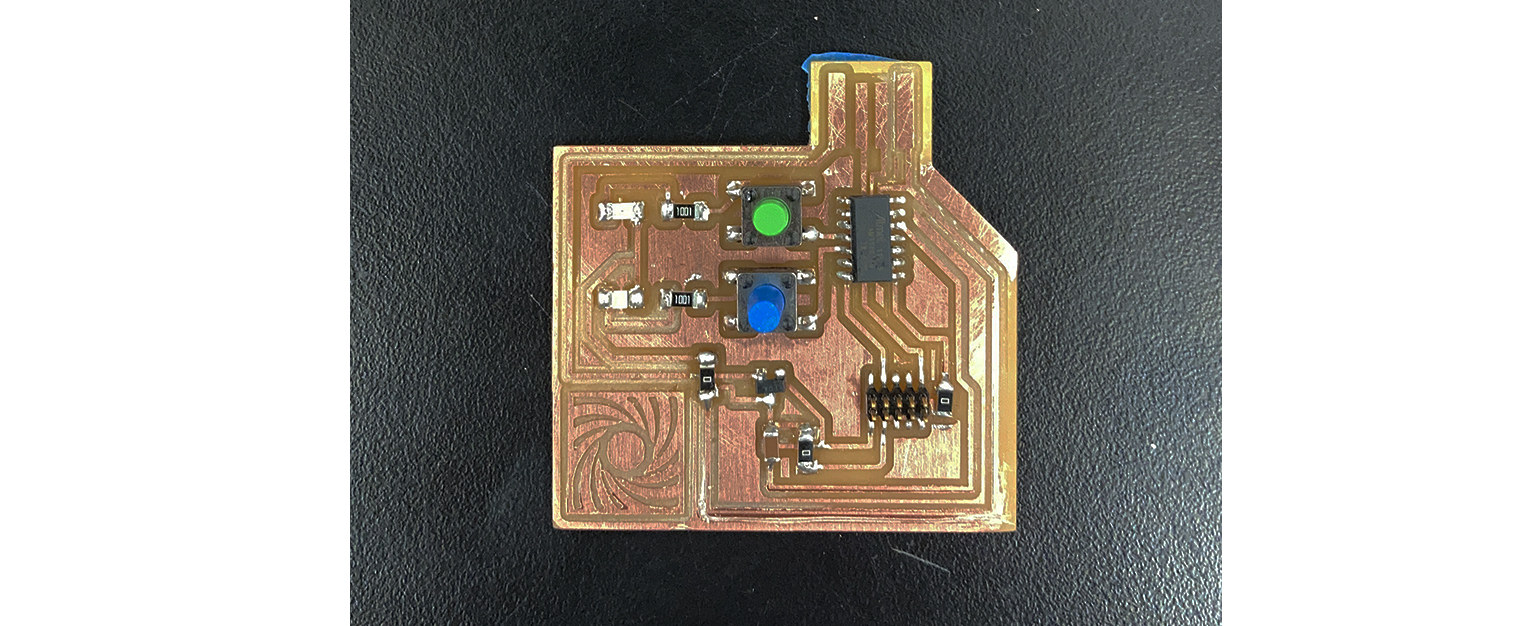
The individual assignment of the week was to redraw an echo board an add at least a button and a diode (LED)(I took the 'at least' part very seriously and ended up adding two buttons and two LEDS)
The first step was to determine which ECAD software to use, which was way overwhelming than I thought. After seeing Quentin and Leo's software in the recitation, I first was very excited trying their software but since Leo was not going to be in the lab throughout the week, I wanted to feel 'safer' in my decision and be able to watch tutorials if I had to. Thus, I decided to use Eagle, a PCB sofware compatible with Fusion 360. Since I am an AutoDesk user for a long time, it felt like it was a good choice to start with.
After watching the introduction video I found on the ECA site, clicked on the 'new electronics design' and playing-with-the-software process be-gun...
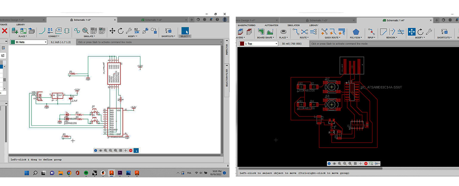 I have questioned how friendly Eagle's User Interface was thorughout all this weeek, even though part of the software made everyhting so simple (accessing the library, checking if there are errors etc.) the other part of it made it hard even to drag the components from a place to another at times. The week was also about adjusting to the software, since I was working with two tabs that had to be synched (schematic and board view).
Let me explain how it all went step by step:
1. Designing and Deciding What Board to Design:
1.a. I first downloaded the fab library, which was shared with us through Anthonny Pennes's mail. I was able to access all of the components I needed.
1.b. To make the process a bit more understable since it was my first PCB Design, I decided to use the microcontroller chip ATSAMD11C board, instead of the tiny's, which are more intricate to work with.
1.c. I layed all of the components to my schematics tab, and here is the list of all the components I first used apart from the chip I have mentioned:
I have questioned how friendly Eagle's User Interface was thorughout all this weeek, even though part of the software made everyhting so simple (accessing the library, checking if there are errors etc.) the other part of it made it hard even to drag the components from a place to another at times. The week was also about adjusting to the software, since I was working with two tabs that had to be synched (schematic and board view).
Let me explain how it all went step by step:
1. Designing and Deciding What Board to Design:
1.a. I first downloaded the fab library, which was shared with us through Anthonny Pennes's mail. I was able to access all of the components I needed.
1.b. To make the process a bit more understable since it was my first PCB Design, I decided to use the microcontroller chip ATSAMD11C board, instead of the tiny's, which are more intricate to work with.
1.c. I layed all of the components to my schematics tab, and here is the list of all the components I first used apart from the chip I have mentioned:
I. USB Connector: CONN_USB
II. Pin Header: CONN_05x2_ARM_DEBUG
III. Regulator: VR_REGULATOR-SOT23
IV. Capacitor: CAP_UNPOLARIZED
V. Diode: LED
VI. Resistors: R_1206 (both 1 ohm and O ohm)
VII. Button or a Switch: SW_SWITCH_TACTILE_6MM (a confession: I tricked the system and used another one)
VIII. 5V, 3V and GND to regulate the power dynamics within the board (not components but connectors, we shall say)
1.d. A night dedicated to adding nets: I spent some time trying to arrange a sense-making schematic. I decided to add the buttons to different pins for them to have different functions later on, and decided to use a fancy LED, which had RGB diodes. Then, I thought it was too risky and changed all of it again. (I know...) Next time, next time. I also added my LED's to anaglog pins at first, but then learned that they should be connected to the digital pins (P14 and P15).
1.e. Routes: I moved from the schematic view to the rendered board view. This part is one of the parts that took most of the time for me, since I was not used to design with such components. I ended up adding two jumps (0 ohm resistors) to connect the routes correctly. I also checked my design rules and changed the clearance to 16 mm, as well as changing the thickness of the traces to 10 mm. (Quentin later said that we can even go for 16 when it comes to thicknes.). This step was crucial in regards to making sure that the board was milleable.
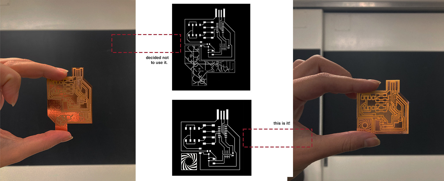
1.d. Here it was: My two button-2 LED board. To export, I followed the display none - activate top layer - export image - display all - activate bottom - polygon - export image steps. I also added the Boston T Line Map to the bottom part of the board, to individualize the design.
2. Milling
Milling part actually took lot more time than I could have ever assumed. I tried for 4 times and the machine did not mill correctly. It was not a file issue, the vectors were seeming fine in 'mods'. We believed that the problem regarding with the artificial layer bening overused, thus, uneven. However, I ended up finding a good milling area on the milling bed and managed to mill one board -which I did not like the way it looked unfortunately. I decided to come to the lab next day and try it again.
I came up with a simpler design this time, and milled it. Only one part of it was not correctly milled but I was able to carve it out with a knife.
 3. Soldering
First of all, Quentin: Franchement.. Merci beacoup pour tous vos efforts. He was extremely helpful during this process and I have learned a lot of details I have not applied in the week 2's PCB-making process. We made my board shiny using the sand paper, we washed it with soap, and made it ready to solder. We also used Flux pen for making soldering easier, which I haven't used before (Should I blame my past mistakes to my lack of knowledge? I didn't know better, I couldn't do better)
4. Checking if the Board Works
Quentin checked if my board was programmable and being read as a USB, and IT WORKS! Now, I need to program it with Arduino.
 Overall, it was a week full of experimenting-failing-learning. I cried once but thoroughly enjoyed even that part.