Week 03
This week I did Printed Circuit Board. The design was ready, I used the milling machine to print it, and I will show the steps of how I did that.
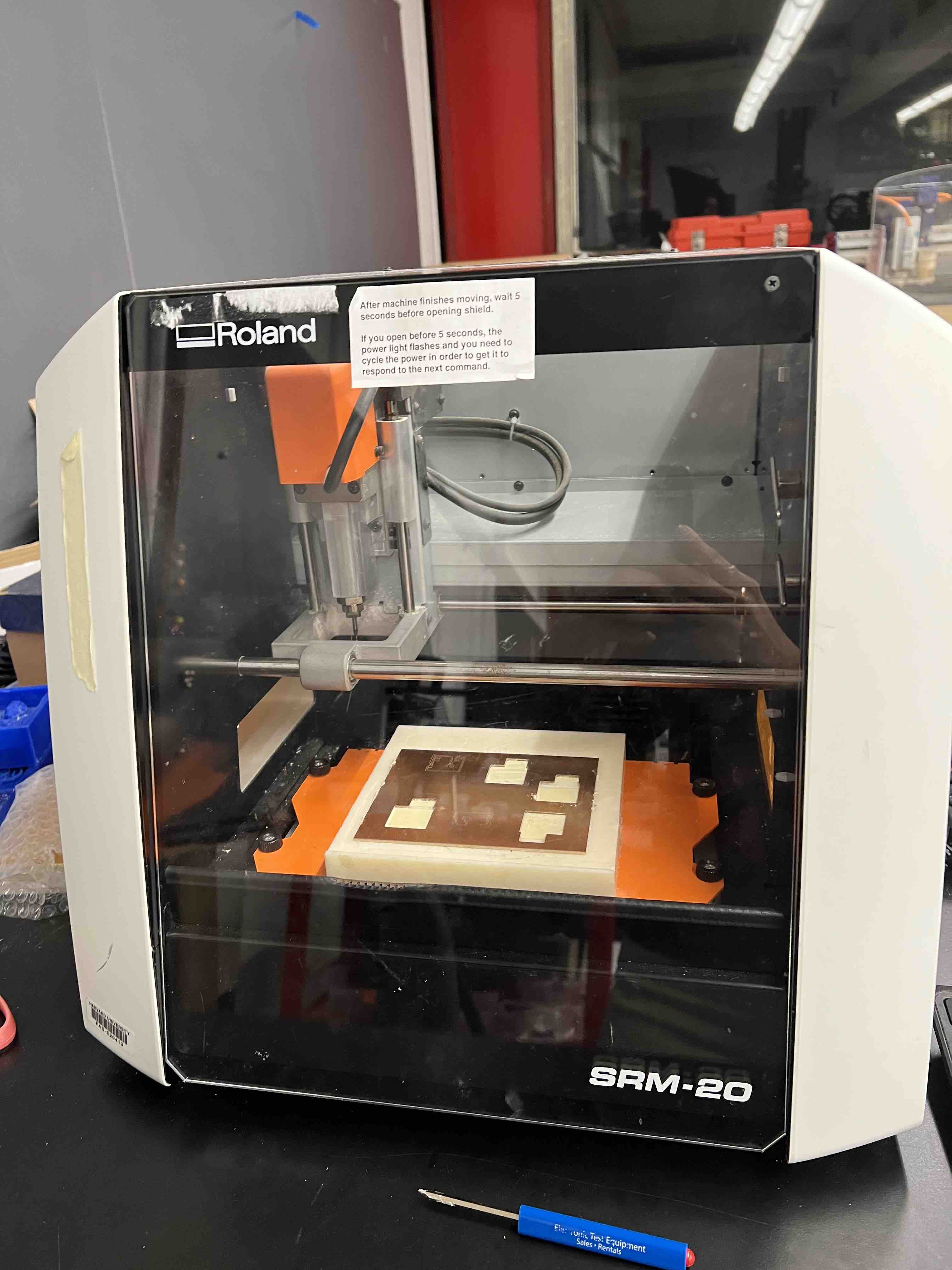 I used this machine at the lab to print it
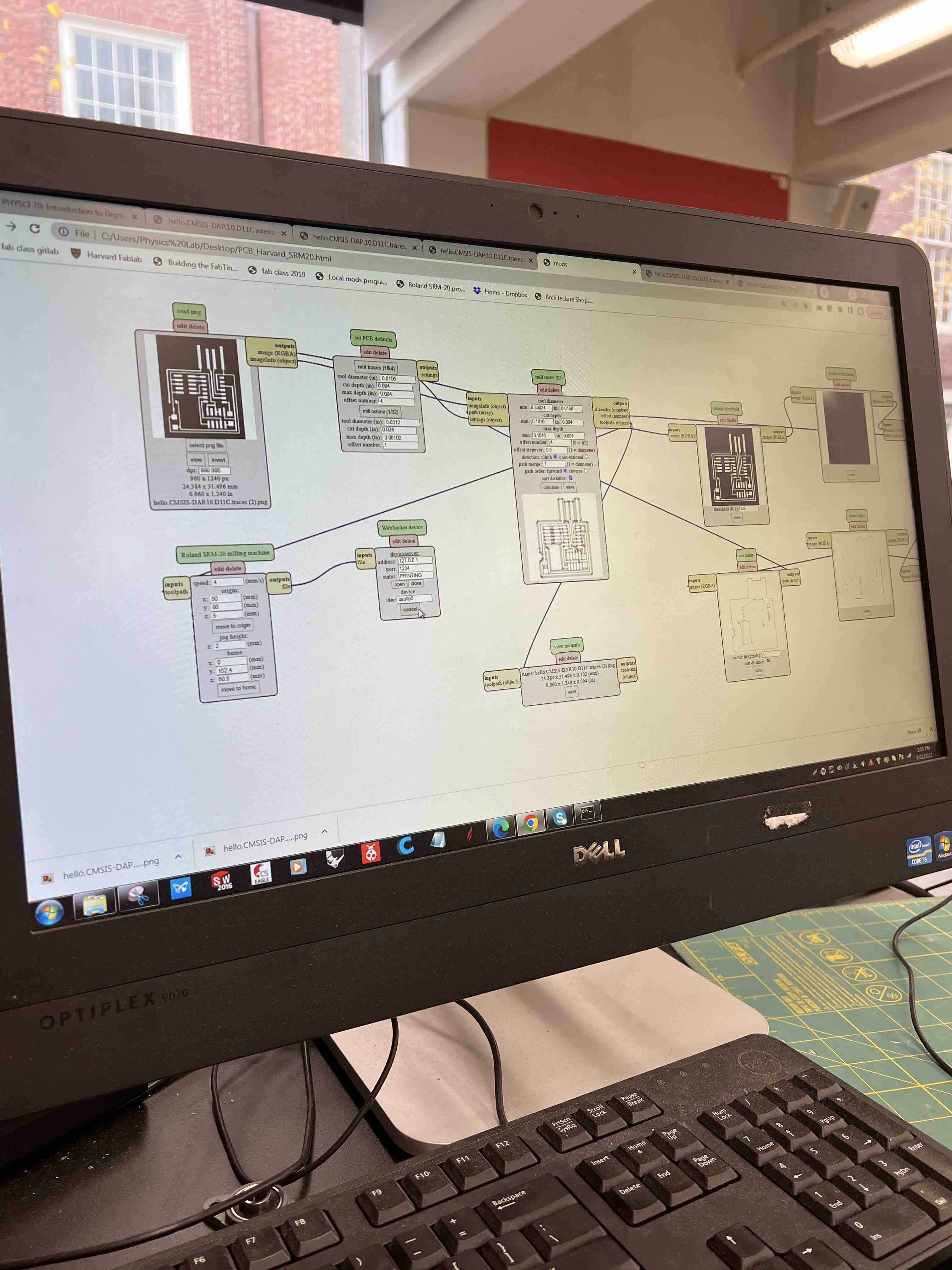 Then I installed the photo shown in the screen and put (mill traces) in thr commands, and then calculated the milling path.
 I used the small size (milling end "pit") to cut the traces, to be able to get all the destails milled, and so it will be small enough to capture the small lines in the design. If I used the large one then it will cut extra and over what I want for the desired design.
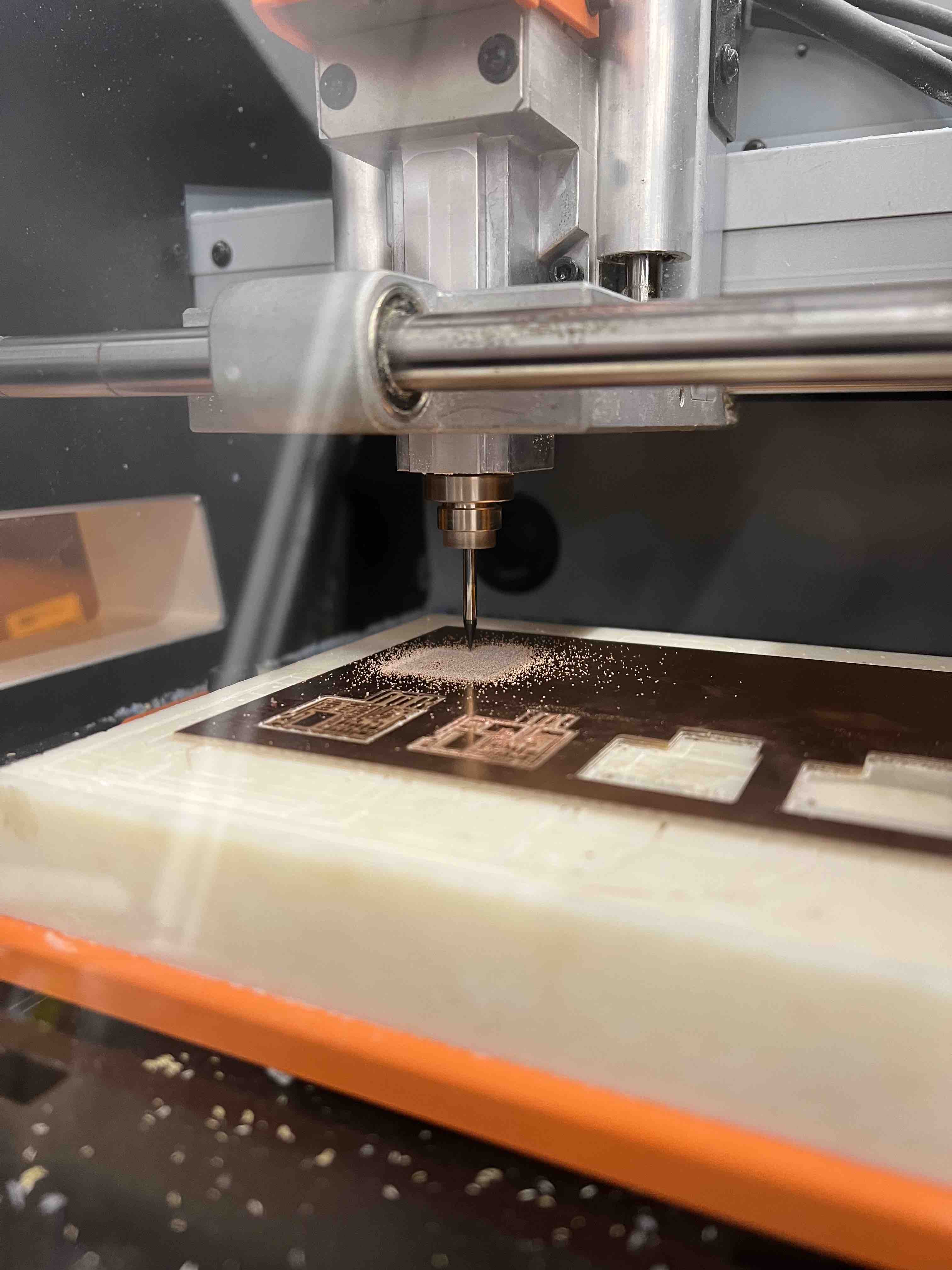 This is while the milling was being performed by the machine.
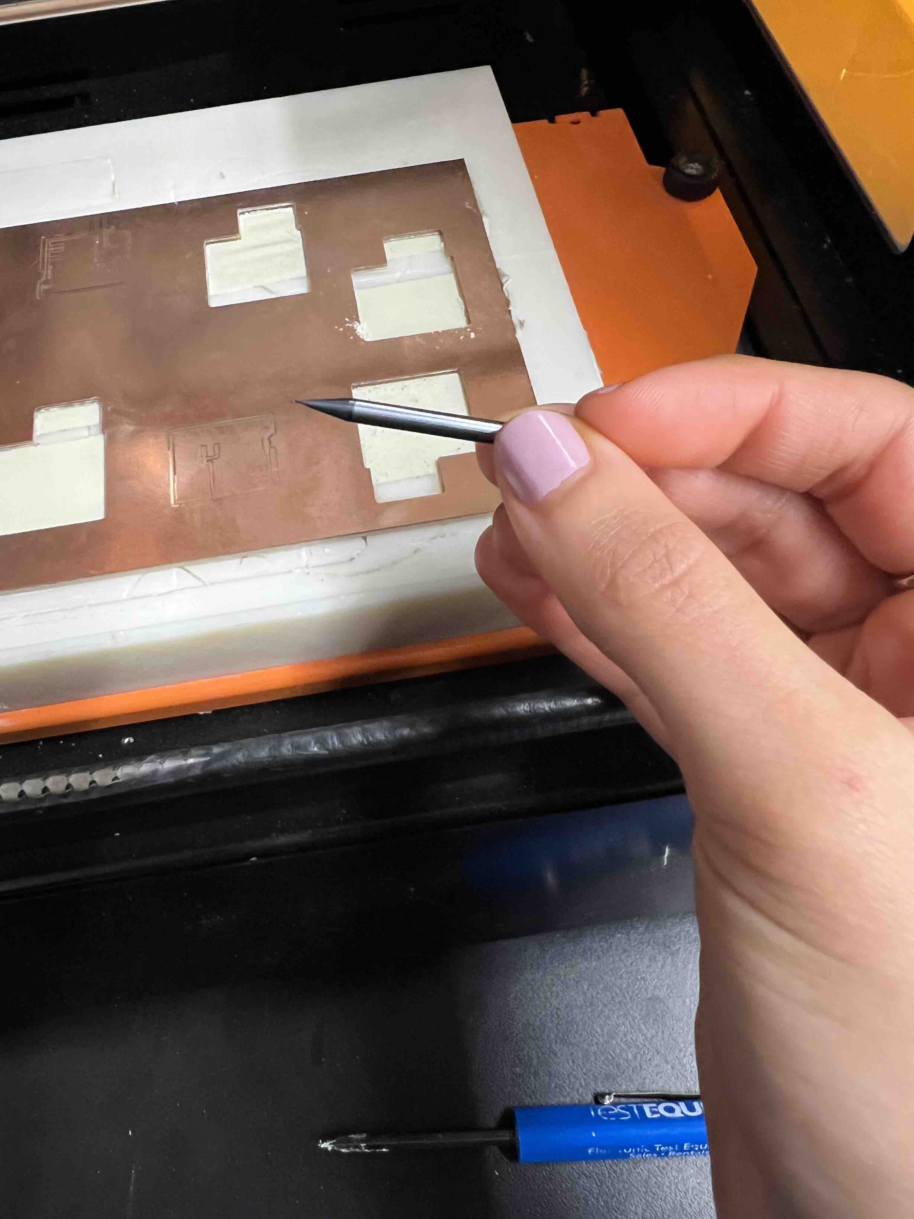
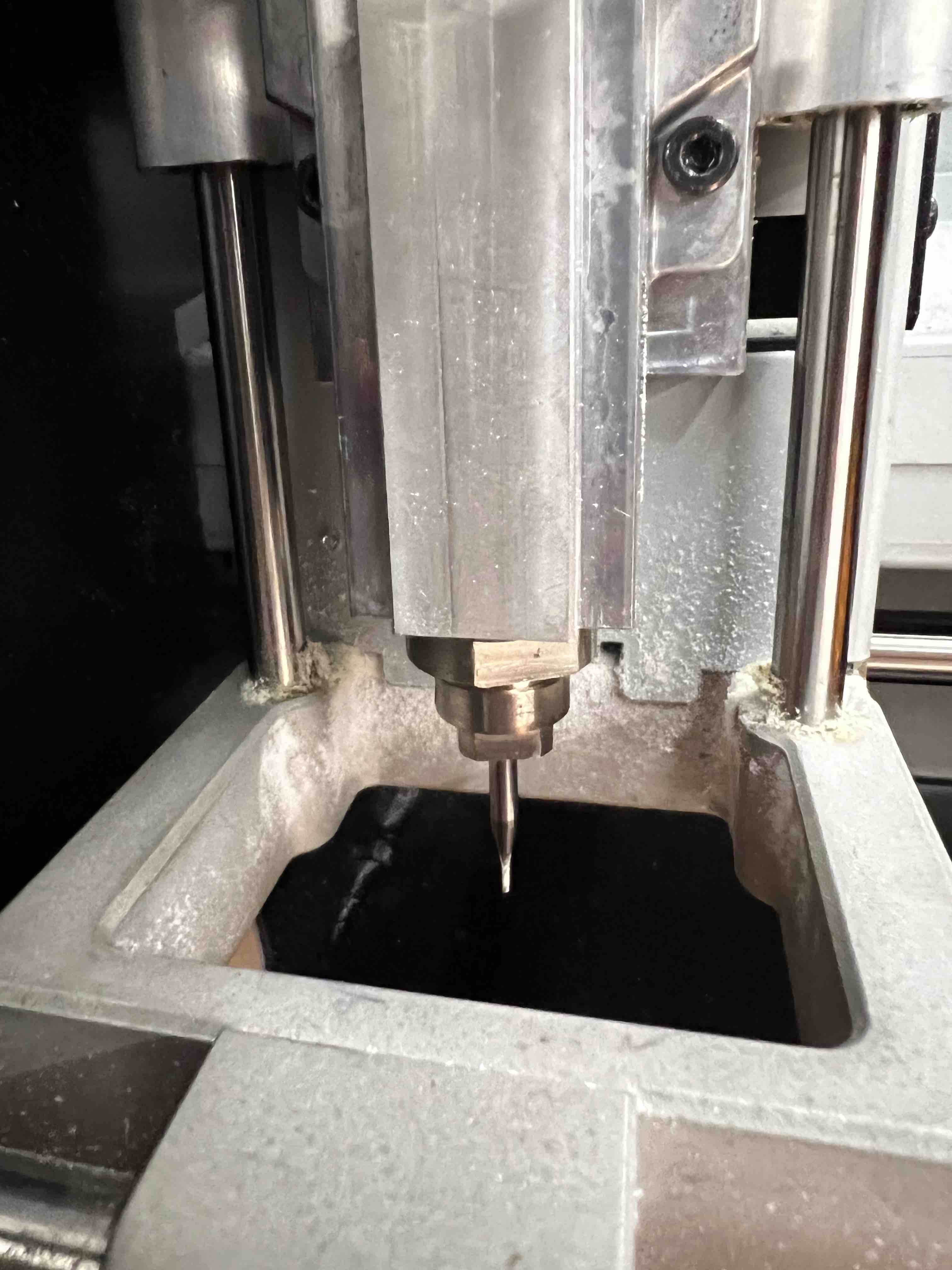 Then I changed the cutting end to the larger size, to cut the outline. I opened the photo of the outline, chose "trace outline" and calculated the path, and started to mill the outline.
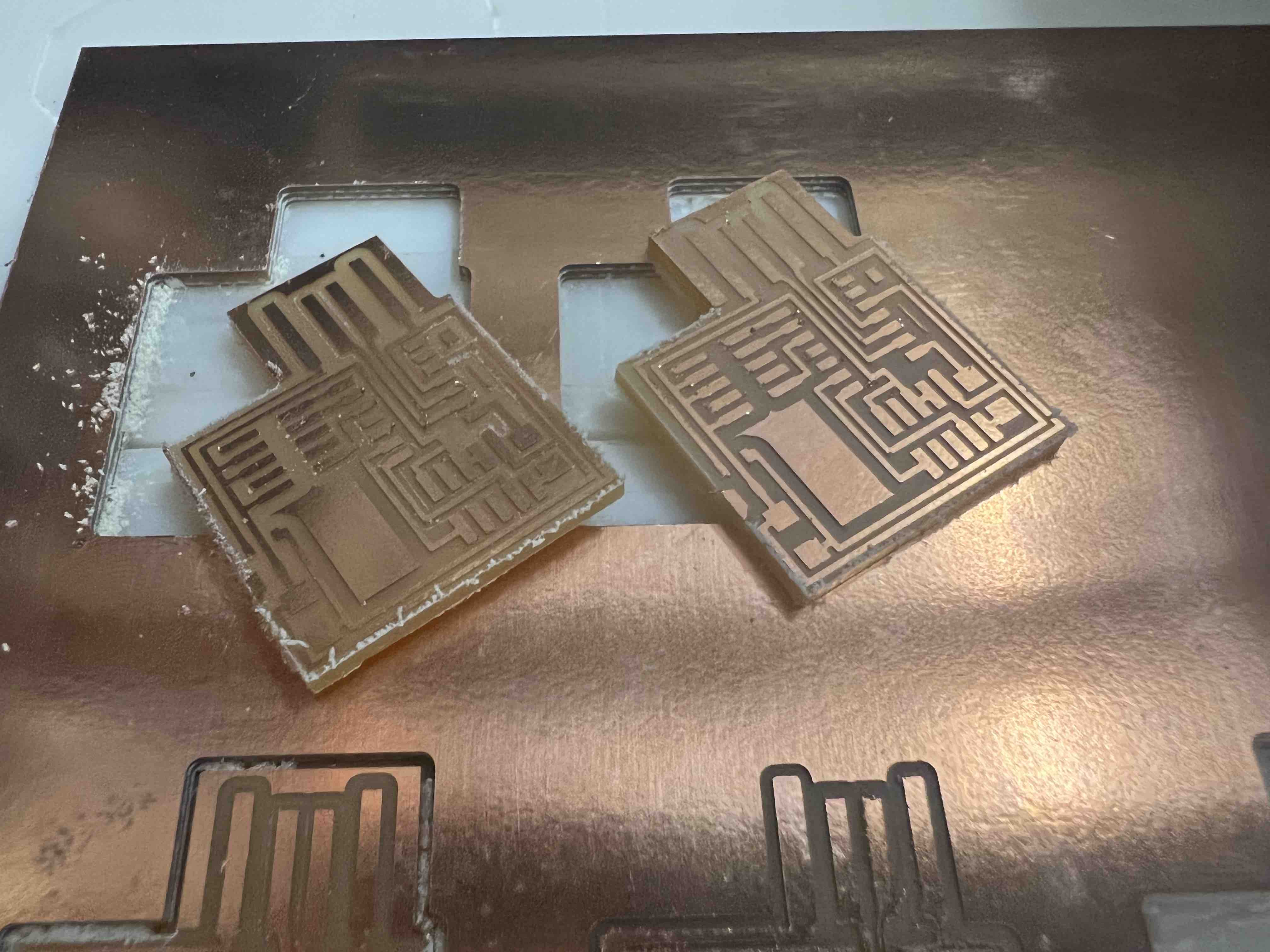
I cut 2 boards to be able to practice and solder all the fine details.
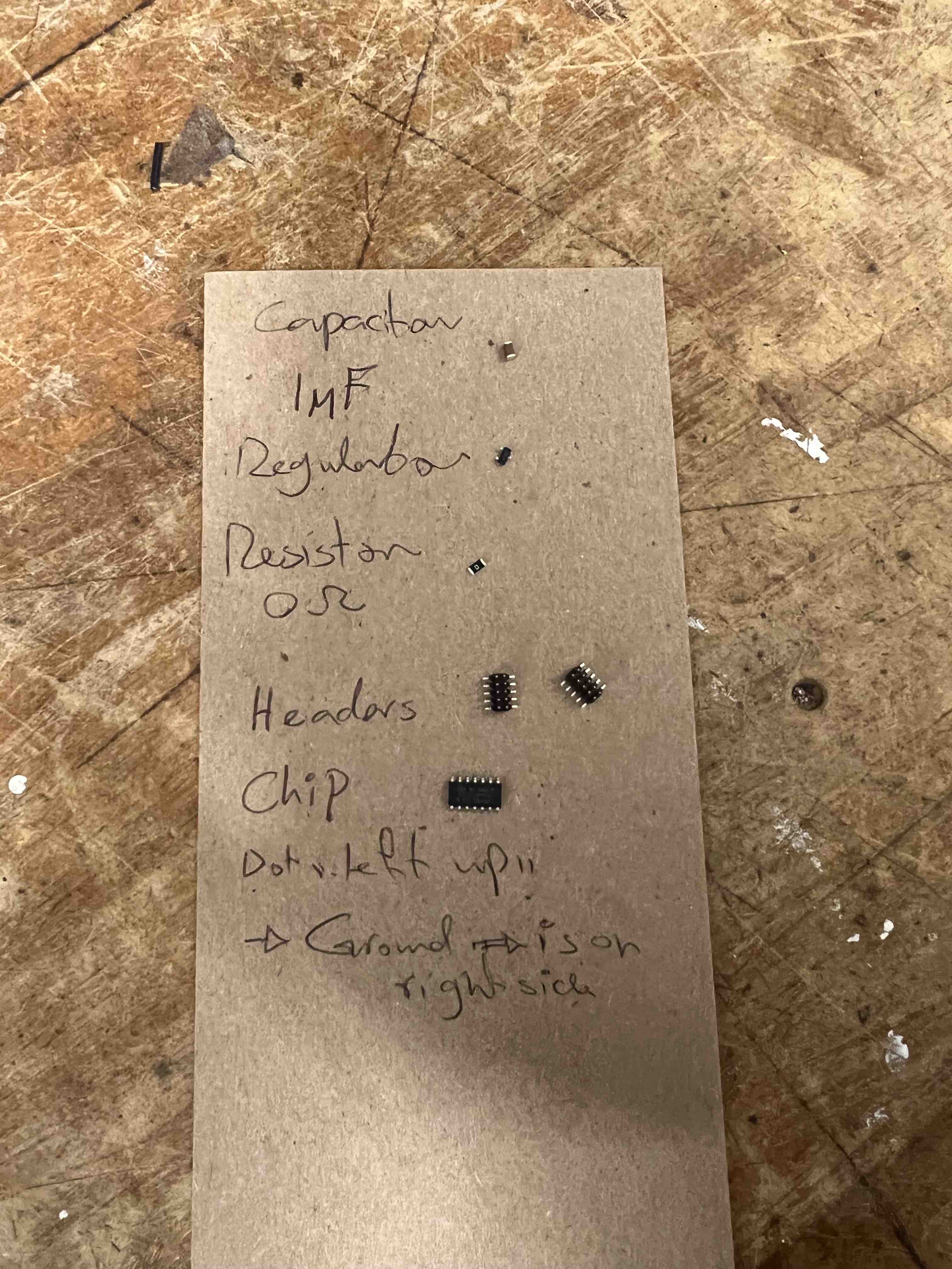 Then I got all the parts to solder them into the board.
 I assembeled this part first, because I thought it's the most difficult part, and then assmbled the rest of the parts using the solder at almost 750 degrees celcius.
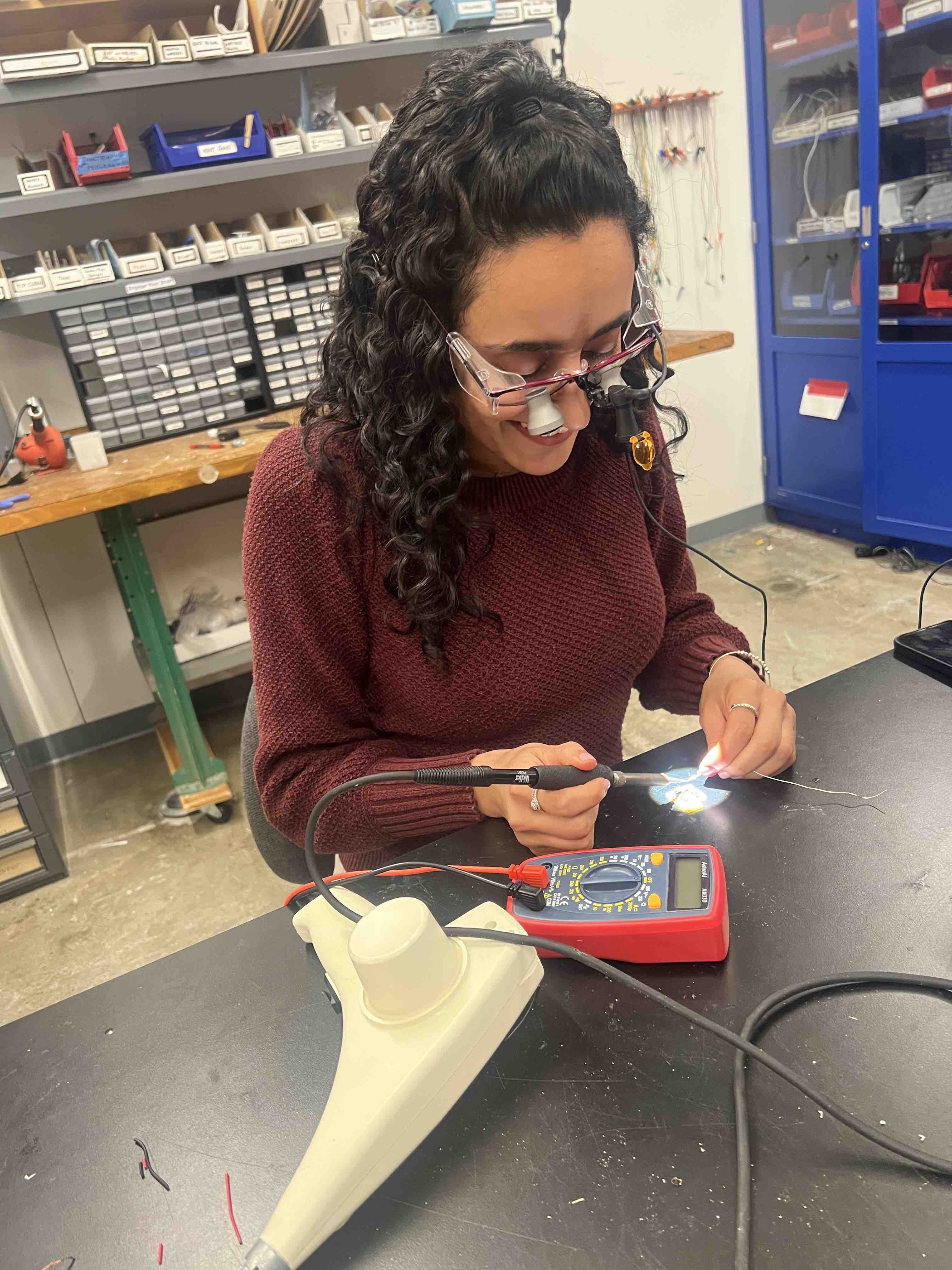 I used my dental luopes to help magnify the field for me to work, and be able to solder on point for all the parts. This was a fun part for me, as Ki had solder dental appliances before, and it related to my tactile skills that I developed with my work in dentistry.
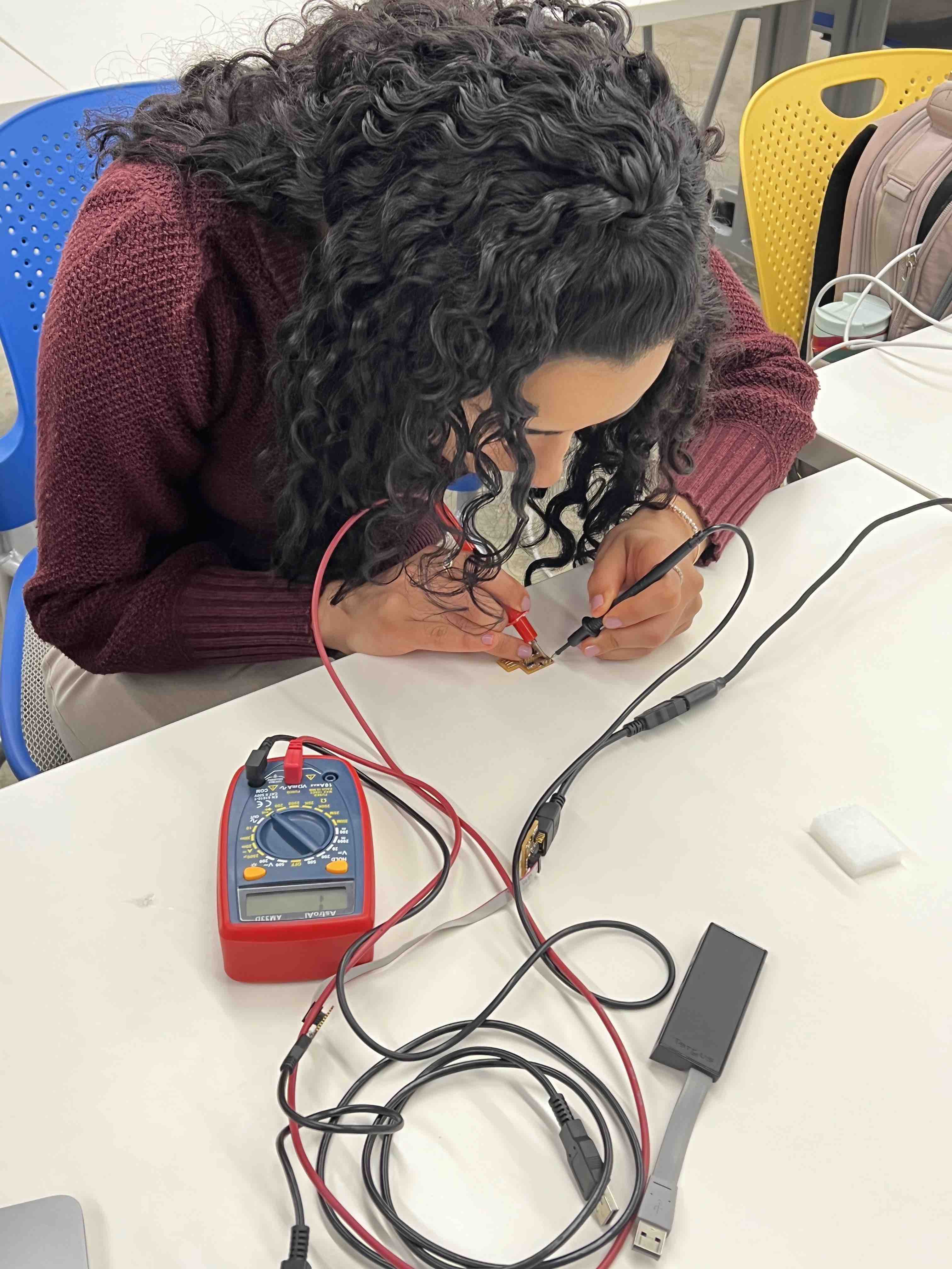 I used the multimeter to make sure that all the parts are connected, and every part is where it's supposed to be. The parts for where ground was showing, and the other connections
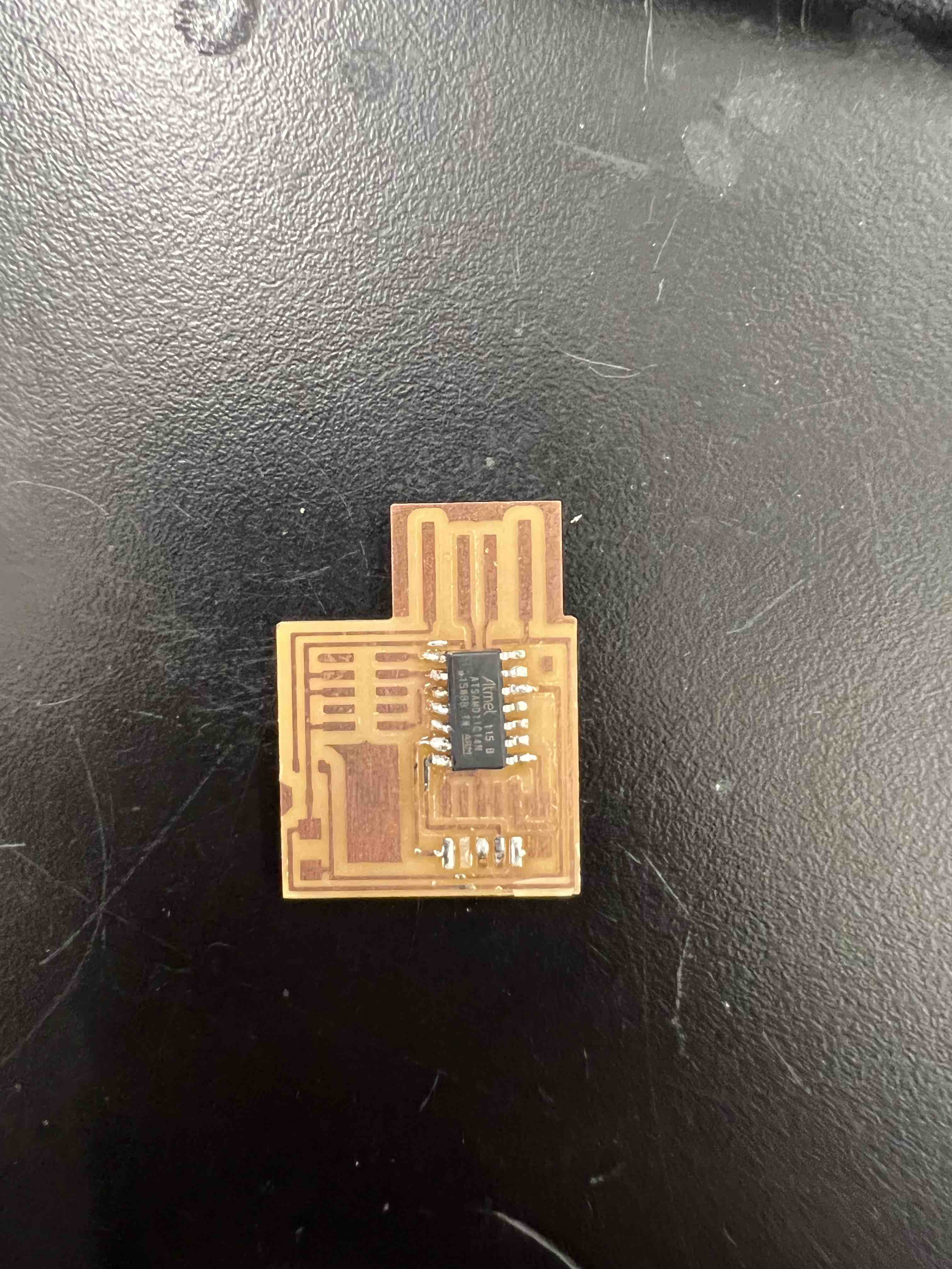
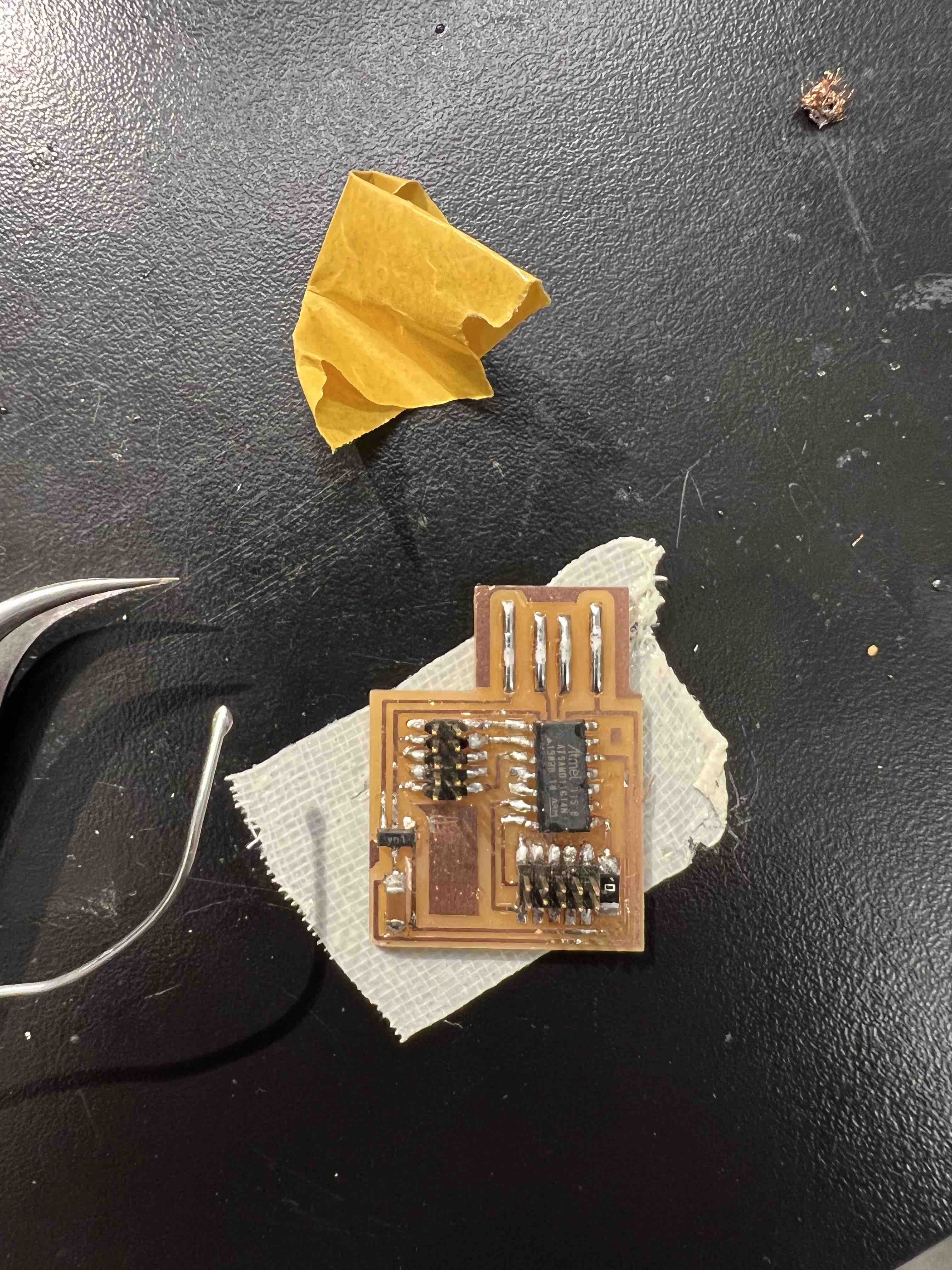 This is the final look after the soldering, verifying the connection with multimeter and the many trails of debugging.
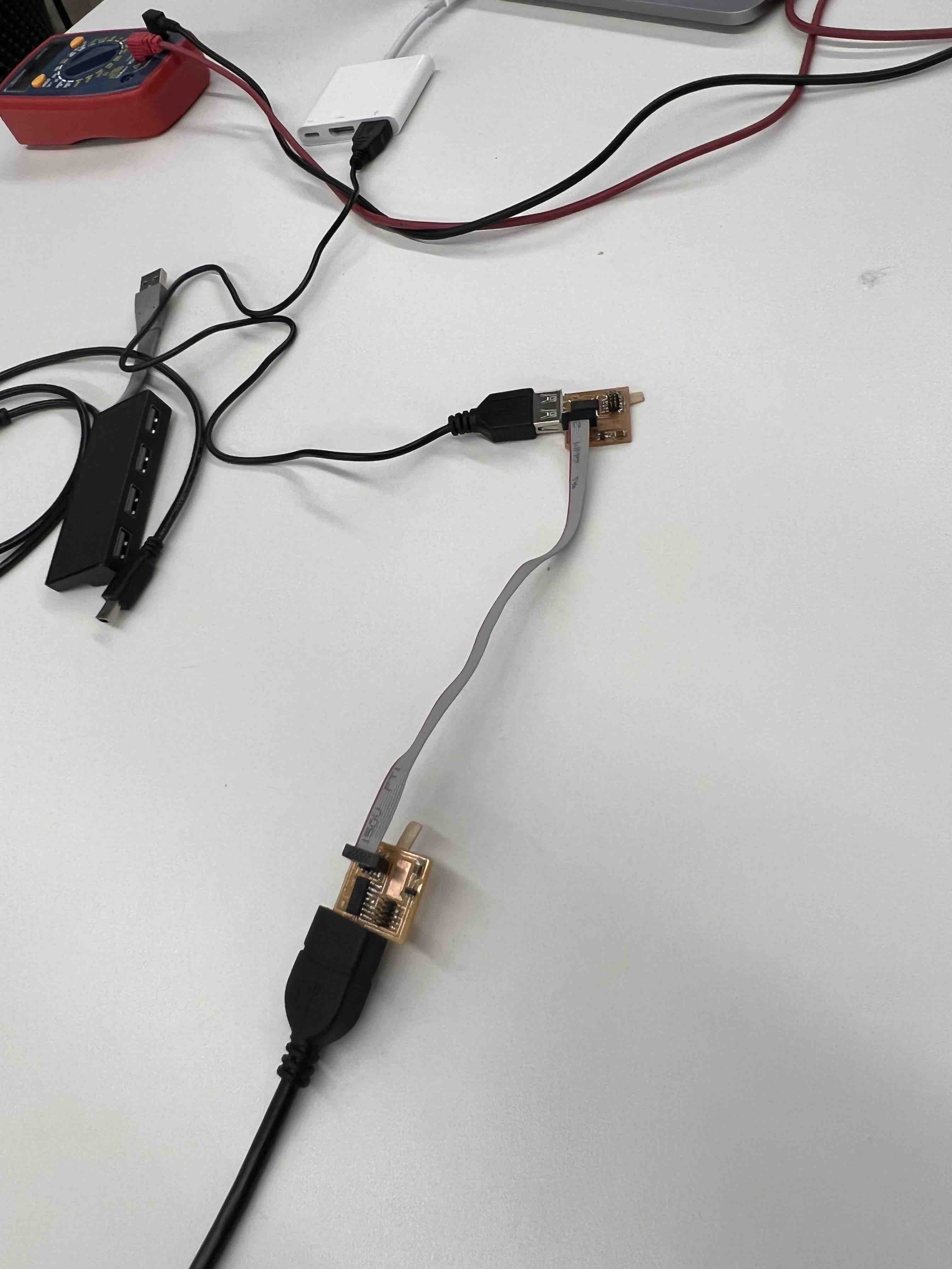 finally, and with the help of our amazing TA Leo, we were able to "program" my PCB, AND have it work as a "Programmer" for my colleagues at the lab!