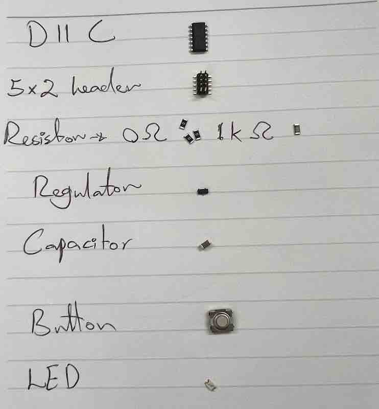
Week 05
This week I designed and built PCB using the D11C with 5x2 header as a guide.
First I started my design using Fusion 360 - New electronic design - and then installed "fab libarary" folder to use the parts in the lab for my design
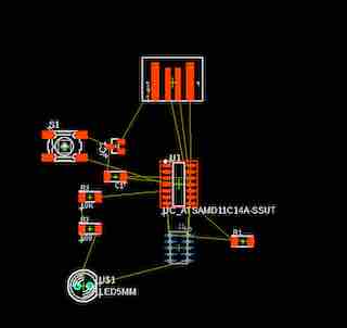
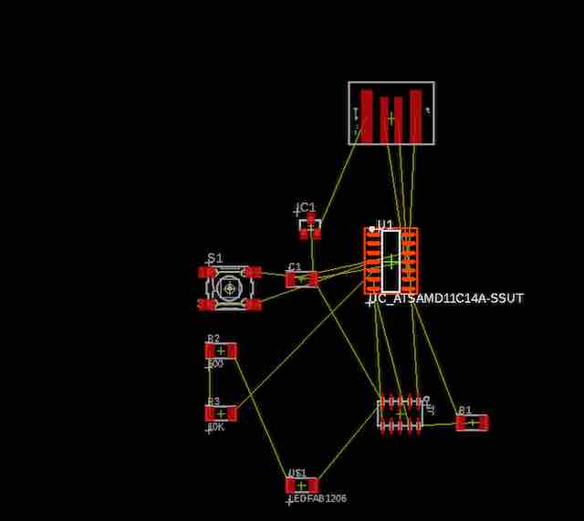
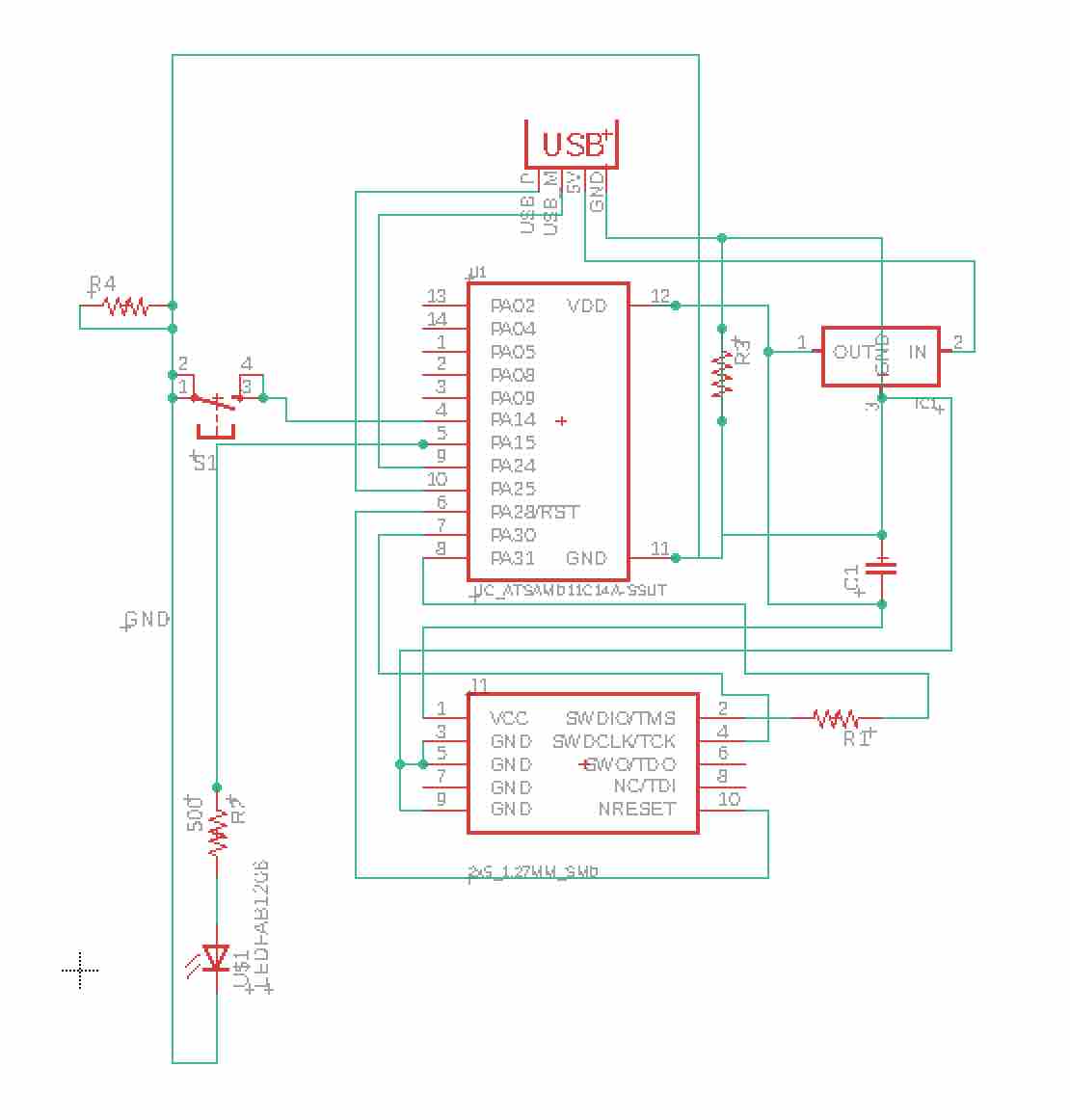
This a picture of the initial design with the components from D11C without adding any other components
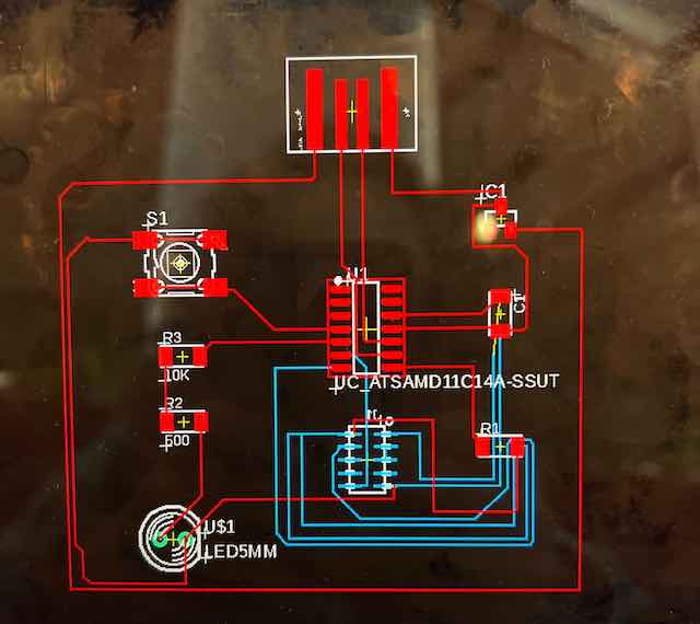
 Then I added the (Button) and (LED) componenets and did the tracing for them.
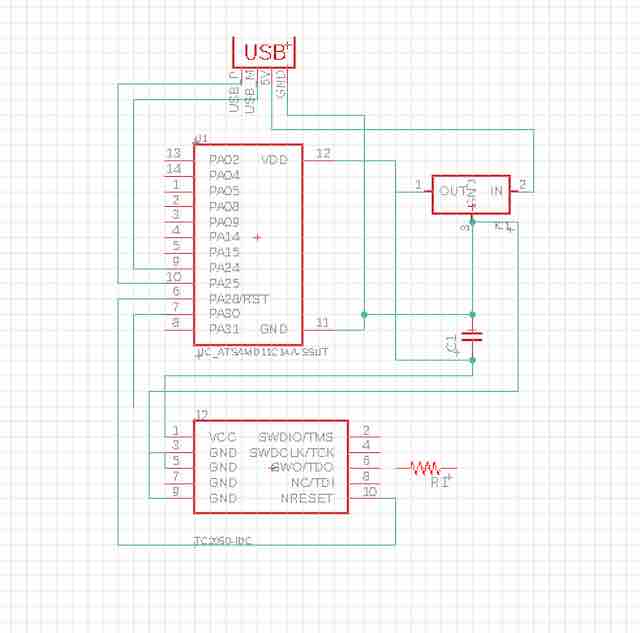
 I clicked on (switch) button in the schematic where it transferred the components to the other view to do the actual tracing for the milling. Notice the 5x2 header component is colored blue (I didn't know that but it means it's in a different layer, and I that it was placed in the second layer).
 Before I started the tracing, I clicked on (Rules "DRC/ERC" and put all clearnace to be 17 mil. I made the tracing, but I knew there was something wrong, so I went to the lab and I found out what it meant and I had to put it in the original (Top) layer.
 I did not want to delete my work, so I clicked on (mirror) to flip the whole schematic, but it changed everything. Even though it brought the 5x2 header to the top player but everything was flipped. And because it was my first time making PCB, I decided to stick to the regular setup of the components so I can trace back in case anything went wrong.
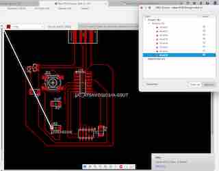 So I deleted the part that was placed in the second layer, and added a new one, and started doing the tracing all over again. I checked that my tracing was correct by looking for (Airwires) in the design. It showed me that I had 9, and it shows exactly where it was placed as you can see in the photo, so I corrected them all, and then finalized my design.
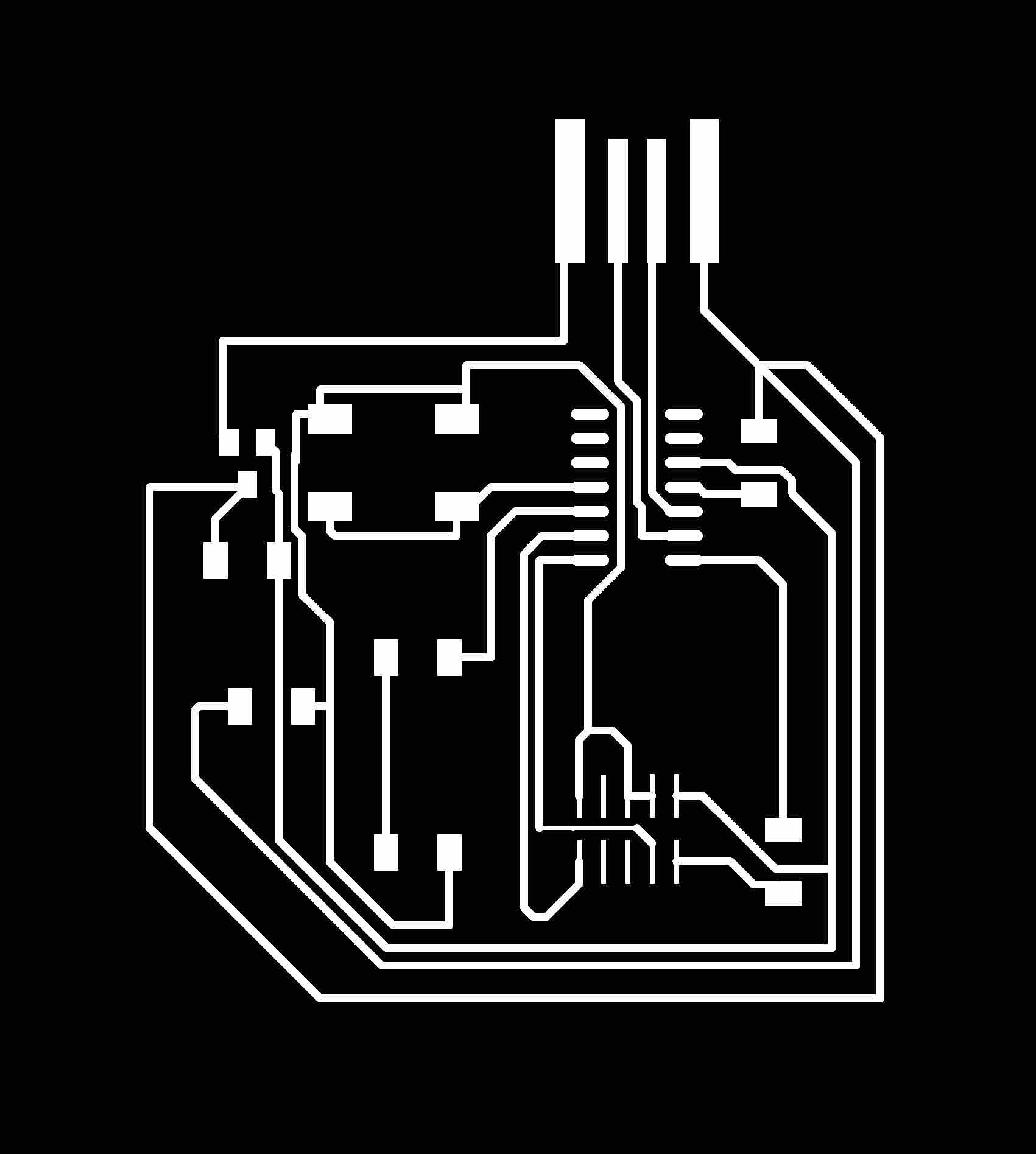
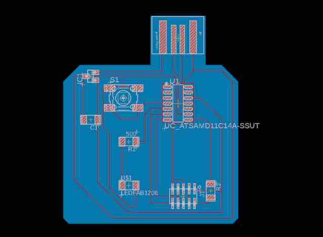 I made the tracing for all the components as shown in the picture, and drew the outline for my PCB.
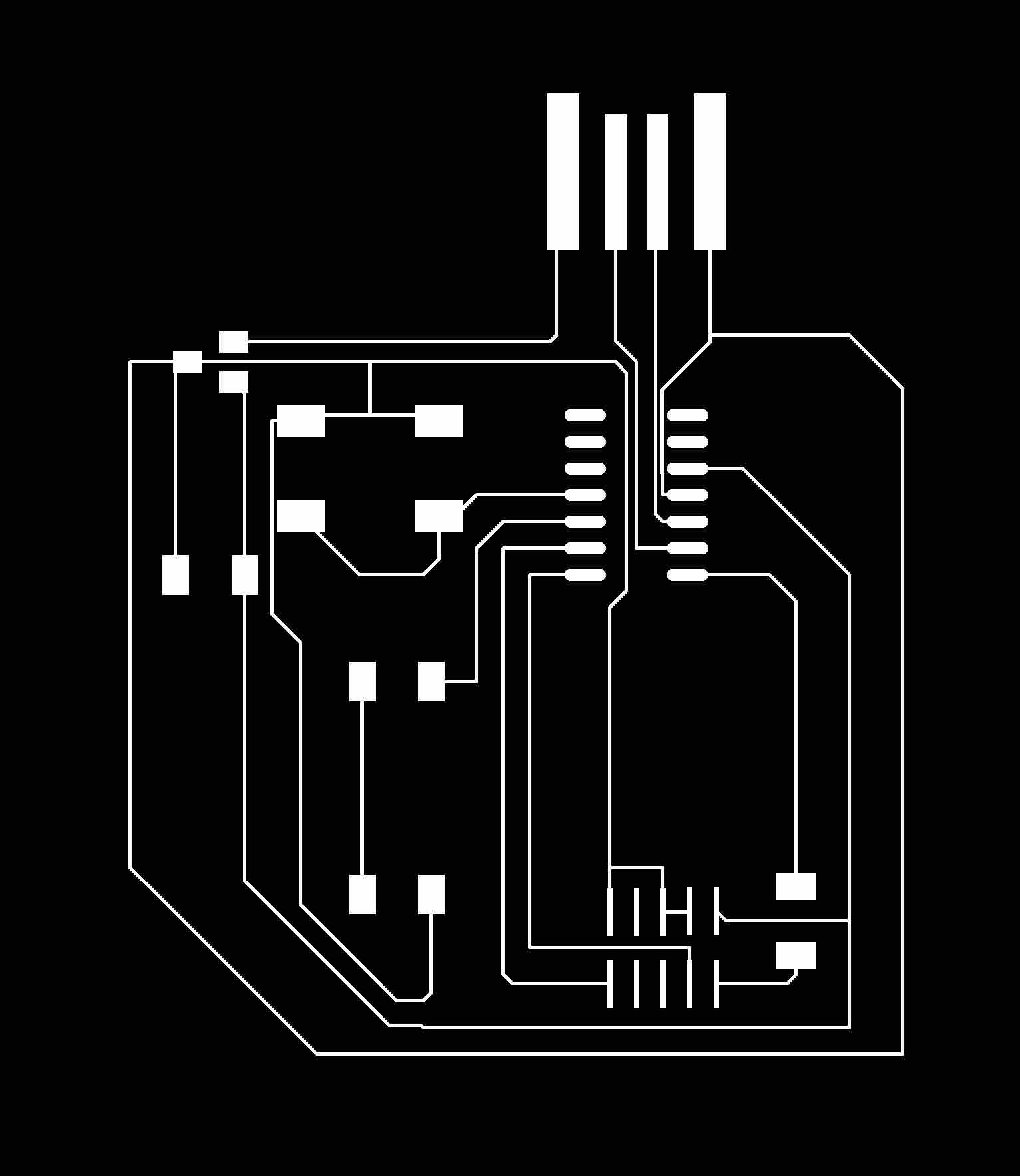 I exported the tracing as an image and clicked on (Monochromatic) so it will be black and white for the milling process to be clear.
 I exported the outline also, and made sure that both of them were matching using photoshop, and saved the image with 800 dpi and as png.
 I milled the PCB, but apparently when I deleted and re did the desgin the (clearance) settings changed to the default which was "6 mil" and that made some of the lines were connected and were not milled, They were very think, and I couldn't make them even manually with scalpel So I had to go back and change the lines thickness and the clearance to 16.
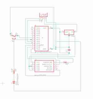
 When I made the lines bigger and increase dthe clearance there was not space for some of the lines to be in the same place I placed them initially so I had to re-do the tracing, and also becase of time I added 0 ohm resistors to bridge some of the areas where I wanted the lines to pass through and connect to their intended locations.
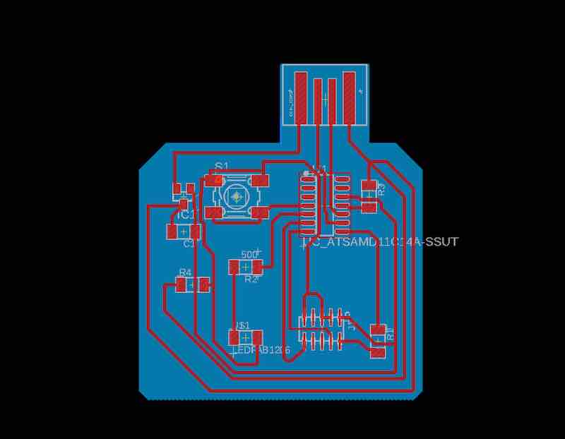
 This is the new schamatic for when I added the resistors and increase dthe width of the lines and the clearance
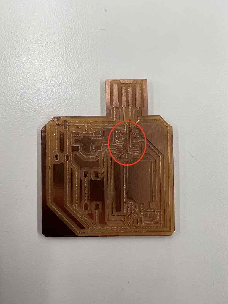
This is a final view of my tracing and design before I did the milling for my PCB
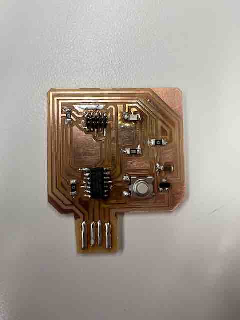
 I got the parts that I had put in the design to solder them.
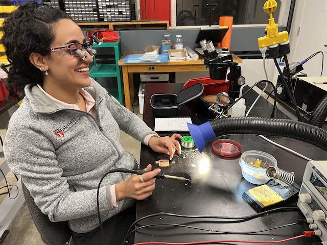 I started doing the soldering for the parts. I used my dental loupes to have a good view of the parts, very convenient!

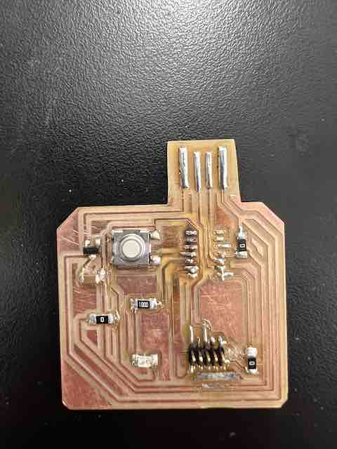
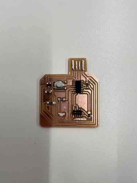 This is final view after I did the soldering
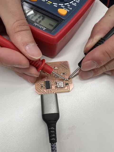 We made sure that it is connected and it reached around 3.28V, so that means it is getting the power through the USB.
 The programming however didn't work so we thought the microprocessor is not working, so Used the heat gun to remove it and add a new one.
 I re did the soldering for the microprocessor and the LED components
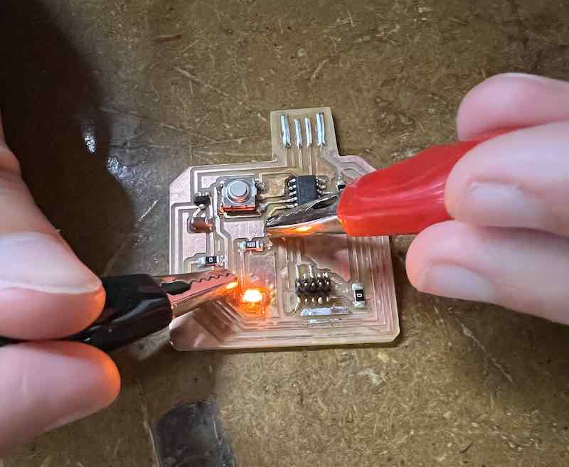 I did not get a chance to do the programming, but I tested it with th Power supply and it lights up!
Group Assignment
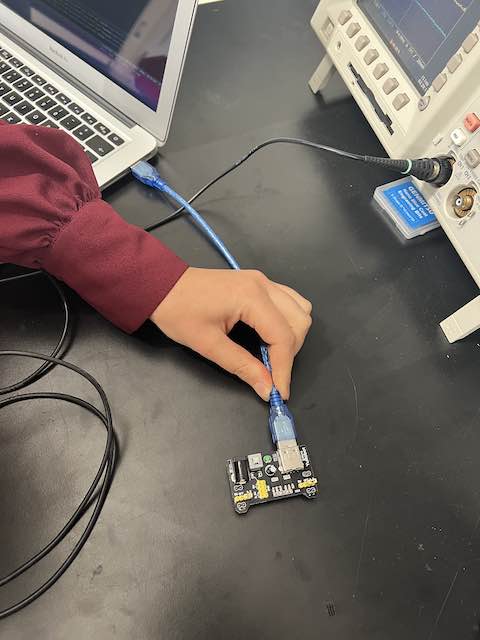 We got the parts to test a functioning PCB
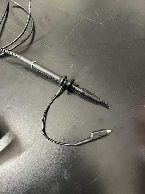
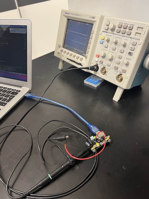 We connected this to the PCB to make sure that 5V passes by the circuit
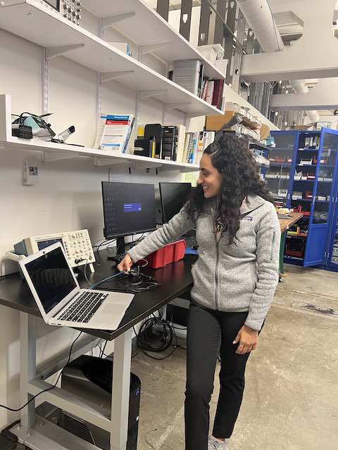 Whe I was trying the coonnection
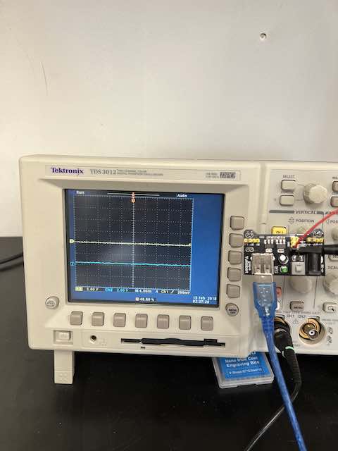 The baseline is at zero when the button is turned off, which measn no electricity is going through.
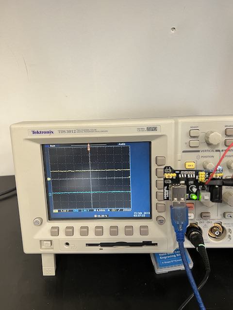 It goes up to 5V when we press the button and the power goes through.