Electronics Design
Board Selection
I noticed this person talked a lot about board selection. For simplicity, I chose D11C-echo, similar to what we did last time. Also, the pins are not very thin (not like D21), so I could probably solder easily.
Design in Eagle (Fusion 360)
I followed Jake's
tutorial as well as this website (There are some components that I'm not sure which one to
use, for example, I don't know the 2x5_1.27MM_SMD, that website gave me a good
guidance). Here are some of the Eagle tips that I wrote down:
down
Move:
- Click “M” on the keyboard
- Align mouse to the “+” cross sign on the component, click, see if it turns brighter
- Move
- If move multiple, first select them using the “window select” thing at the bottom right, then do 1, then right-click on the blank area and select “group move“
Delete:
- Click the “X” on the top bar
- Click the link you don’t want. This will delete it.
Others:
- Use “Net” to create wire (shortcut is "R")
- Use “Name” to name the wire, and also create those wires that can fly.
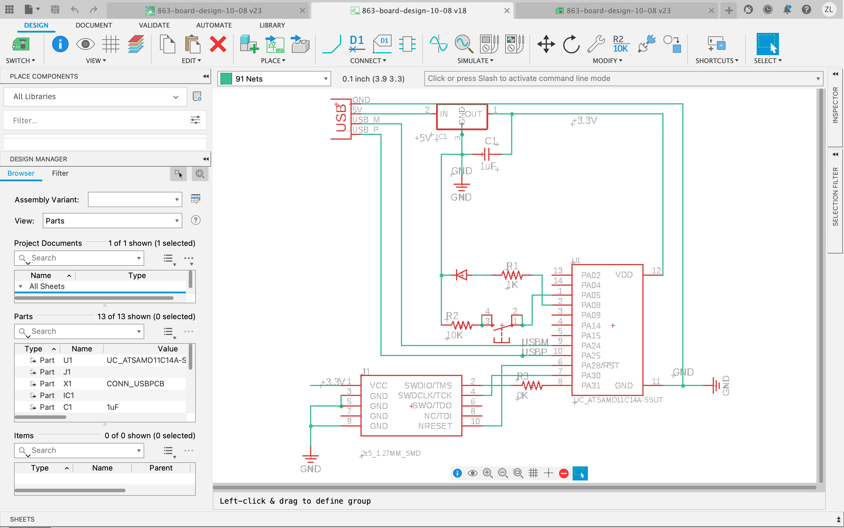
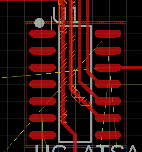
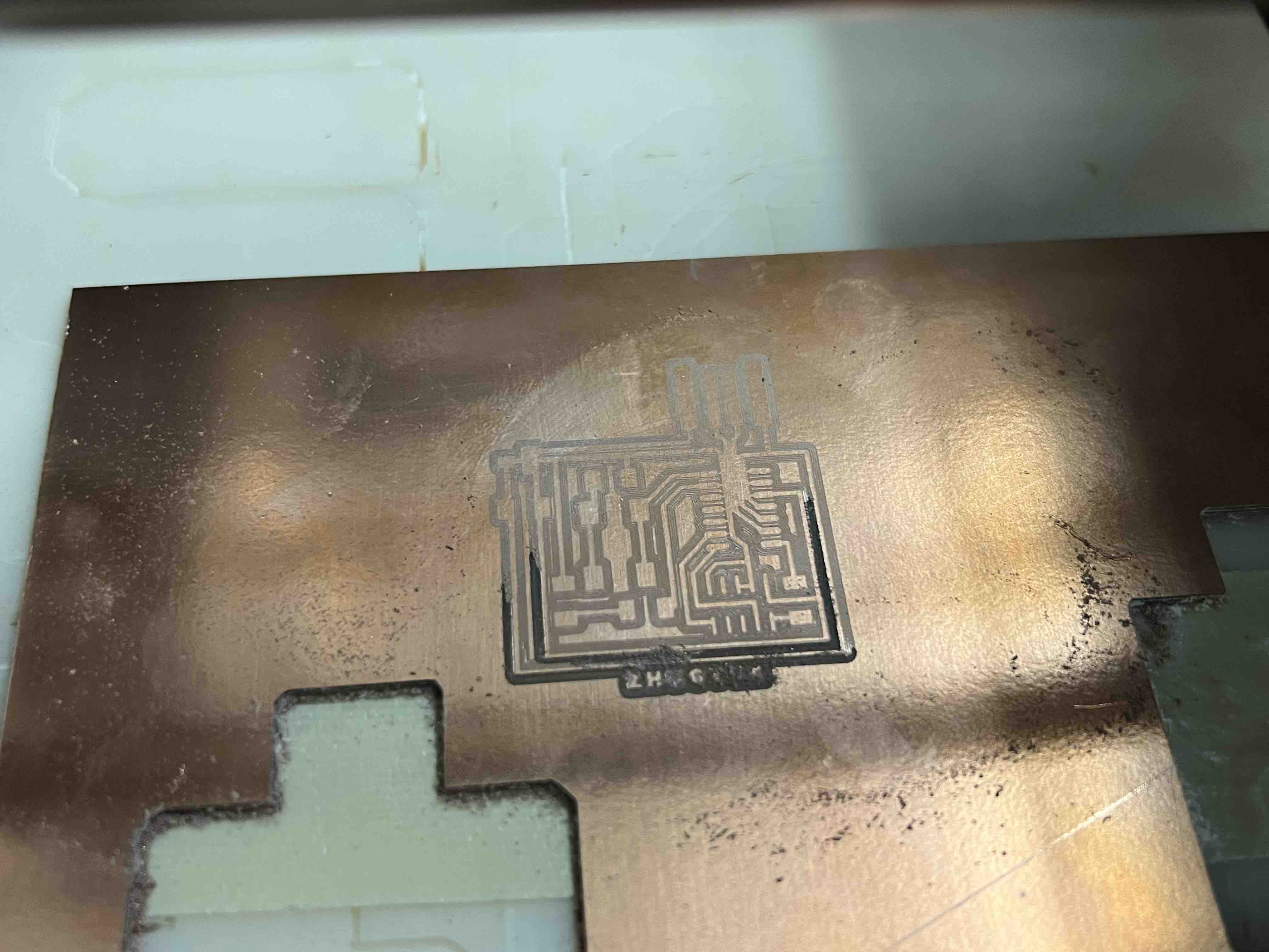
For the routing, the TA in SC 102 told me to stick to the original D11C plan and put the two new
components in the gap between them, so I did that (I used PIN 5 and 8). Also, we were suggested to
use the
fab.dru routing file before routing, but I noticed those four wires under the chip
(yes! the wire can go underneath the components!) were
too close to each other, so I had to lower the limit (I used 1mi) to get through. And I changed them
back before I milled it to check if everything was okay. (Tips: click the "/" key to activate the
command line, type in DRC to check if there are problems in the design)
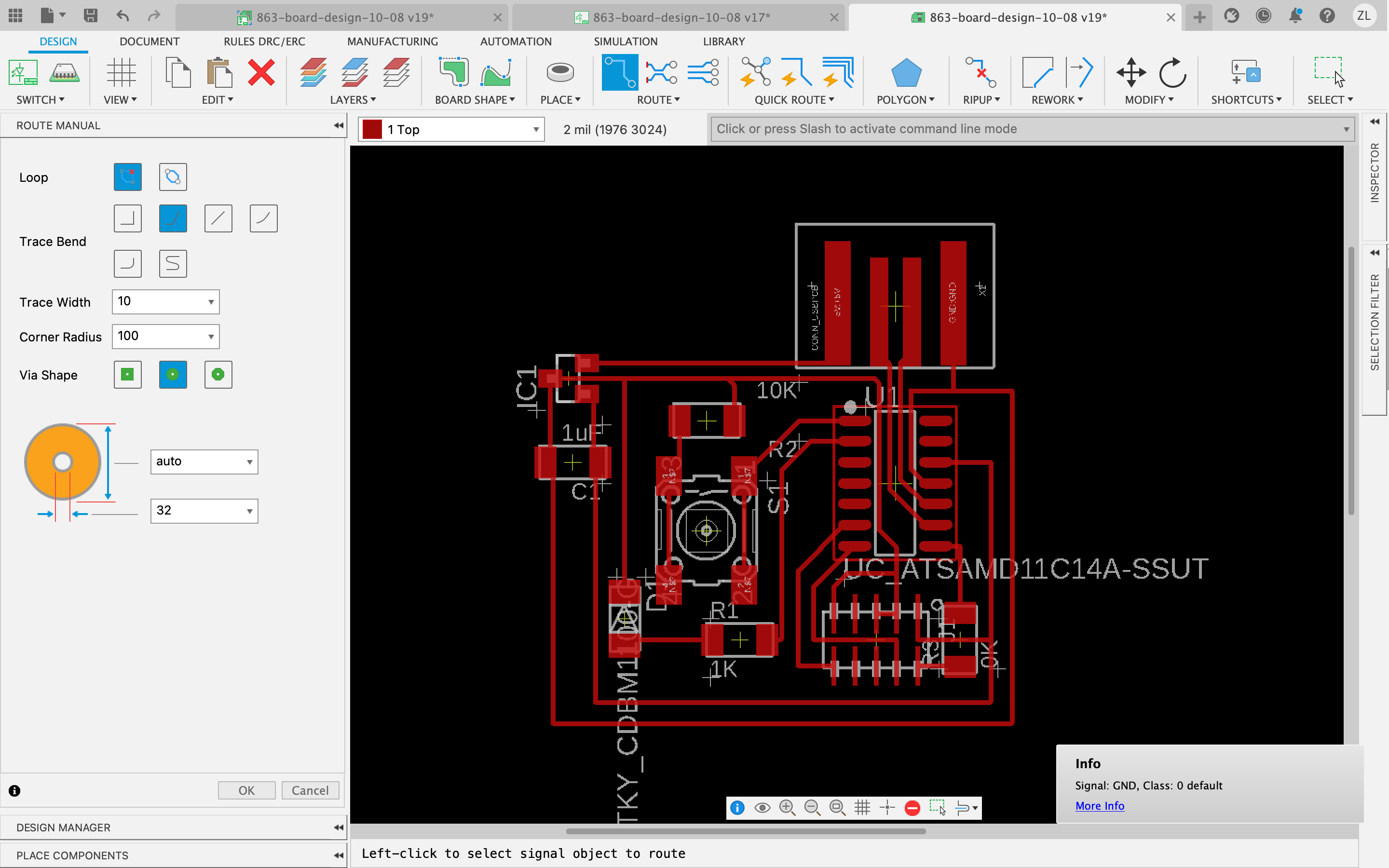
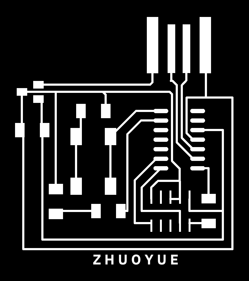
I added my nameZ H U O Y U E to the PNG as text using the Preview app
on my MacBook
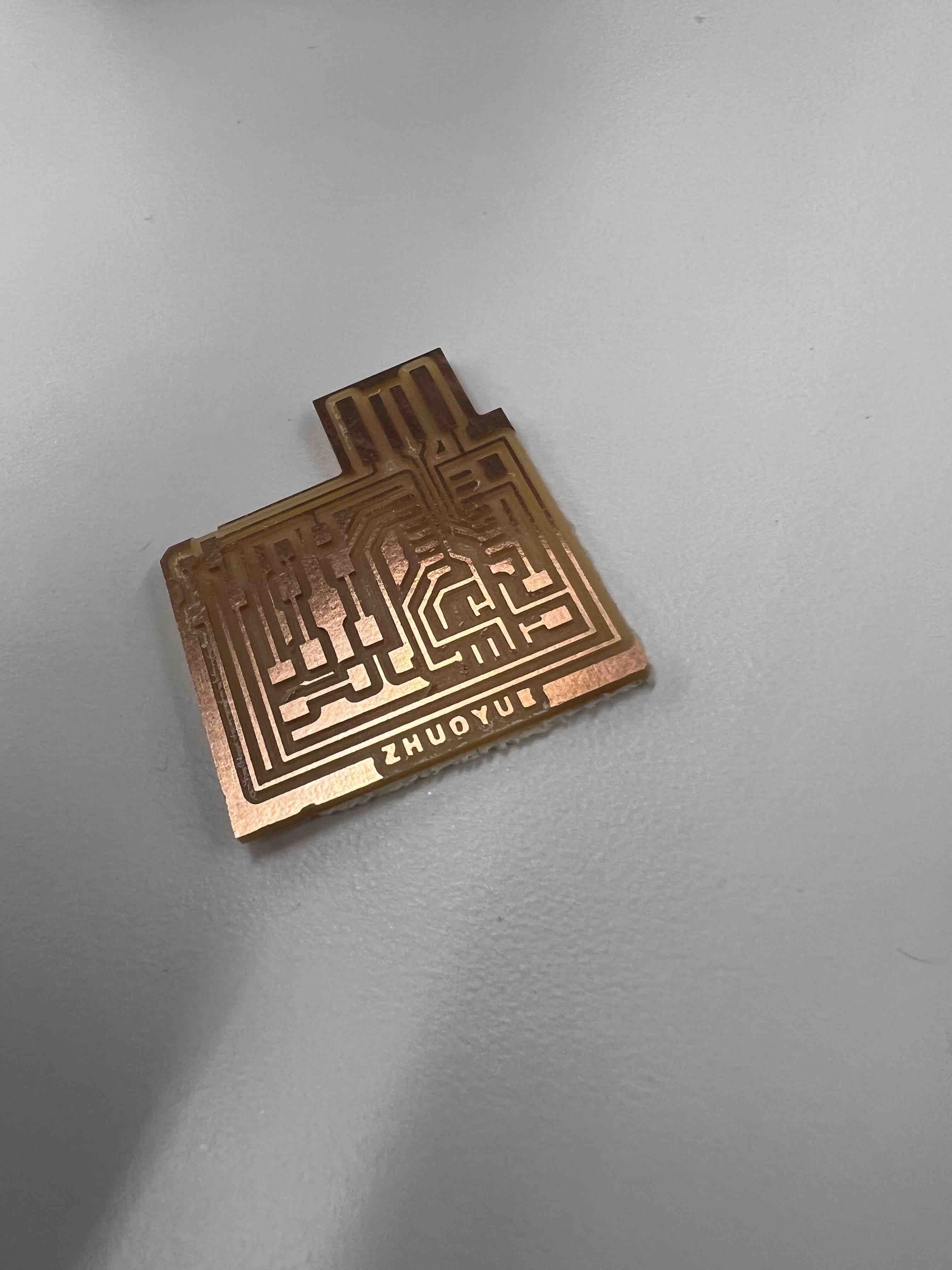
Milling
The first time that I milled, there were some problems
-
For some reason, it was very shallow, and the TA (Chris Zhu) suggested that when I set the drill bit, I should push it as hard as I can. Also, we can increase the depth a little little bit.
-
The four lines in the middle didn't get distinguished. The TA said we could lower the tool diameter, to make the system think it's smaller (but this method has it's limitation, as you will see in week 7, the traces will be smaller than it actually should be, so it's easy to be ripped off. I guess the next time I do it, the better idea is to follow the fab DRC rule. Making it bigger is fine! Instead of try to compress everything), and by checking the
Viewif we see the traces go through the centerpiece then it will be cut.
I did that, and this time it works pretty well!
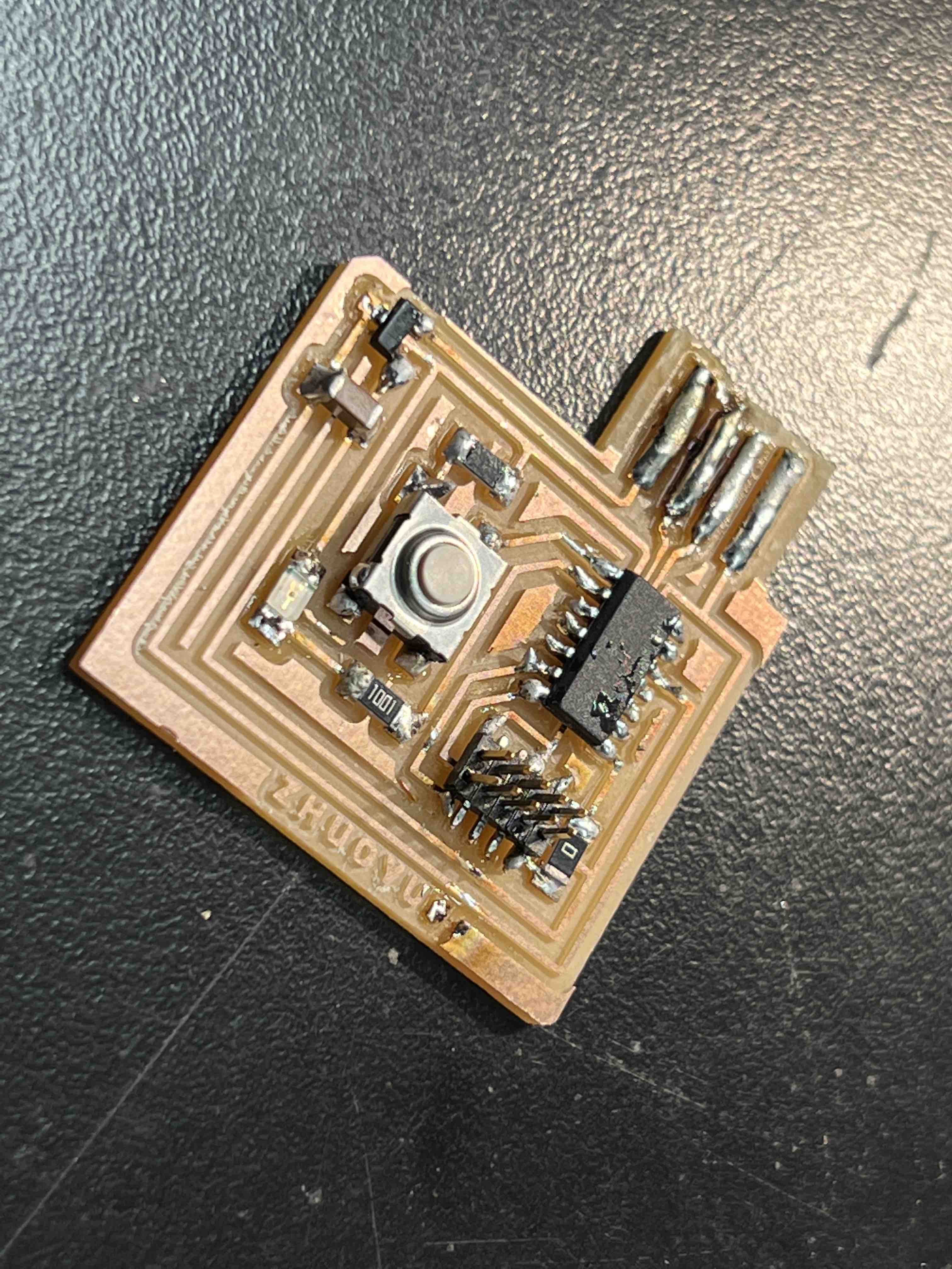
Soldering
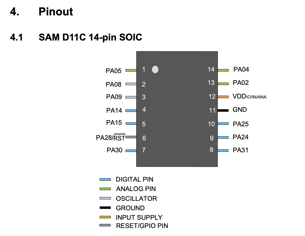
For soldering, you should be careful about the direction of the D11C chip, if you are not sure, the PIN5 has a white dot close to it on the chip:
Also, this website about LED Polarity was super useful for determining the direction of LED! Also, while soldering the regulator (make sure it's a 3.3v one BTW, it looks similar to the 5v one), I noticed the two pads were connected to the wire in the middle, so I maually cut them apart.
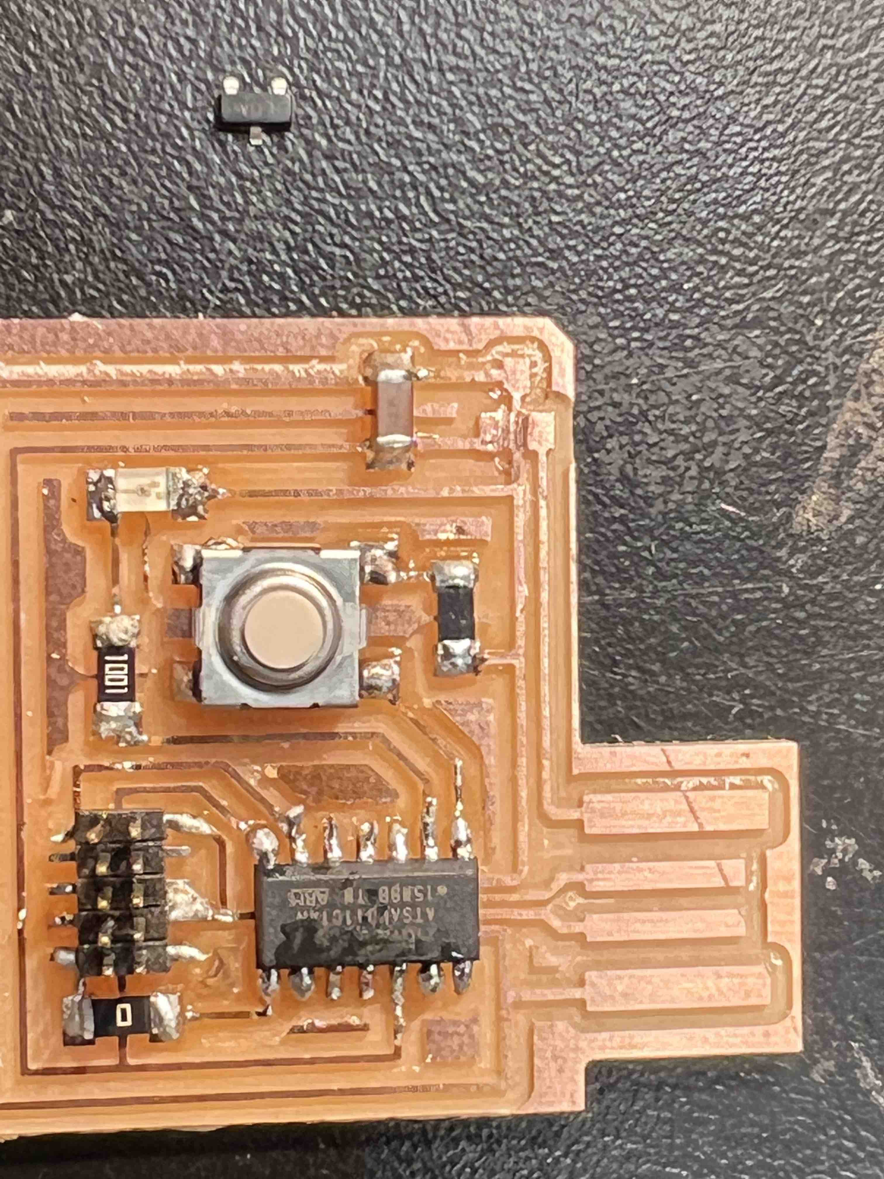
The board looks great!
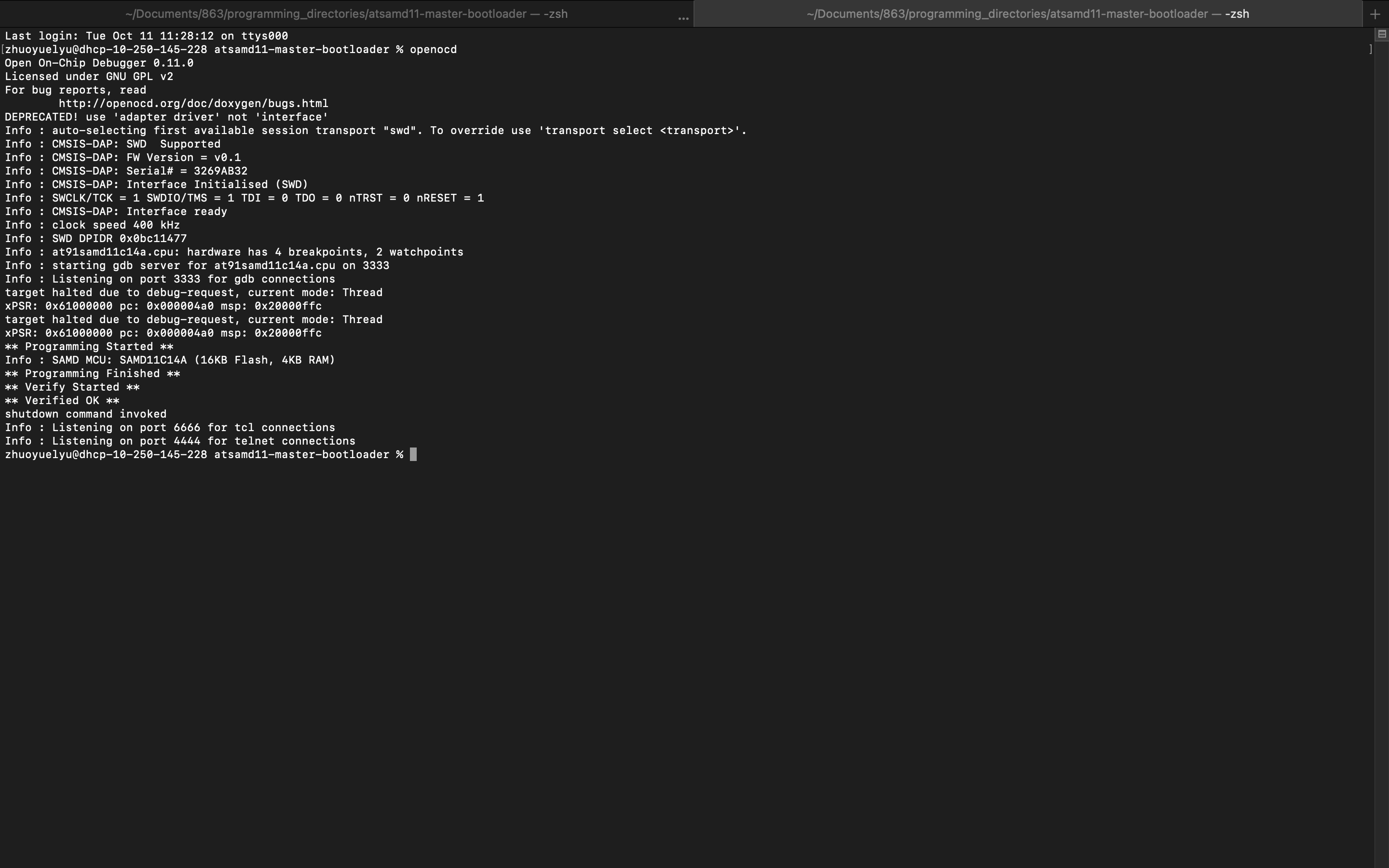
Bootloading
I openocd on atsamd11-master-bootloader(! here, please replace the pin file to this new one ! The old one only bootloaded it
as a bootloader, the one I provided bootload it as D11C! ) and openocd on
free_dap, the
same one we used previously, it was successful.
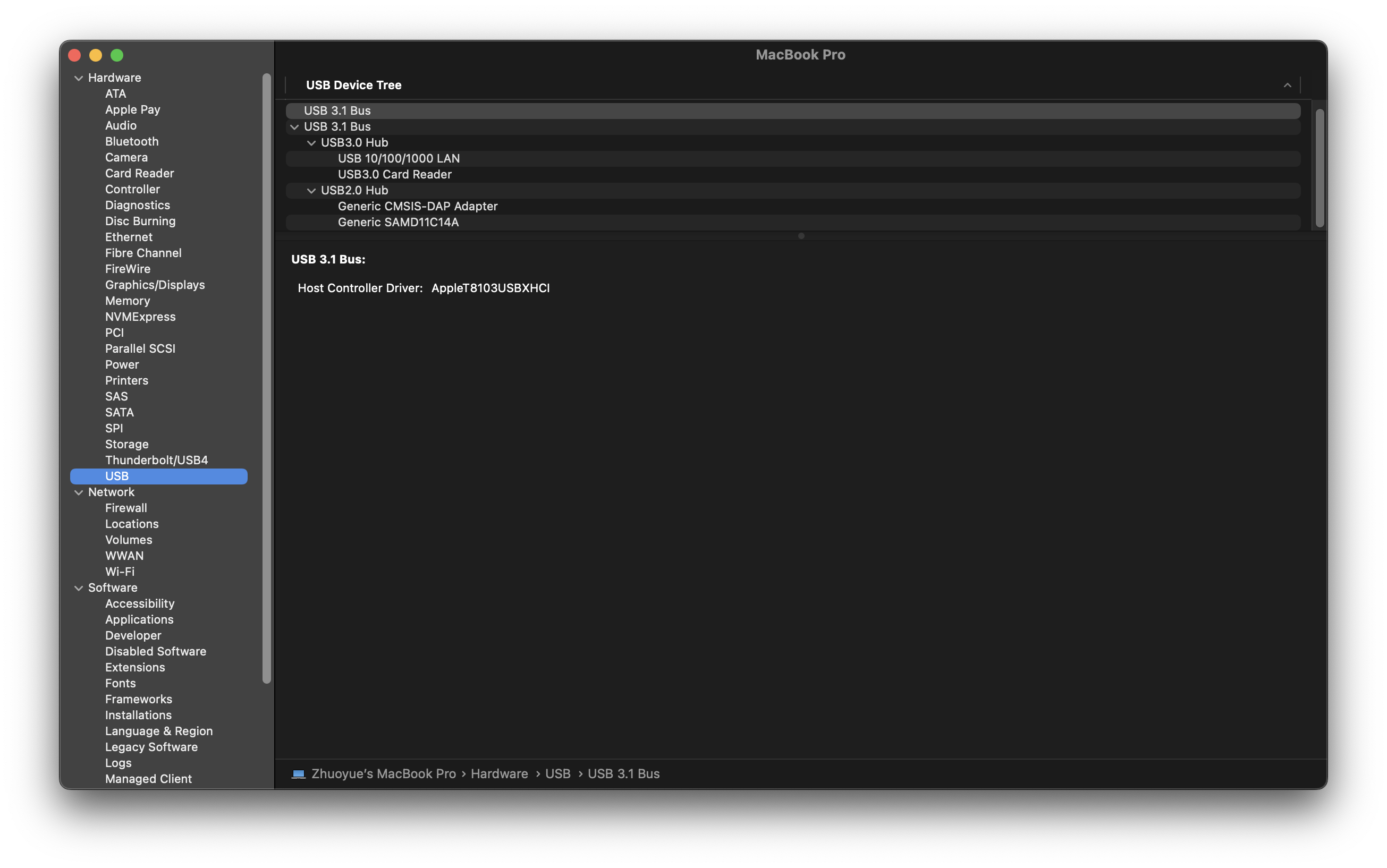
 Your board should be recognized as
 SAMD11C14A instead of adapter stuff
 I continued to program it in week 7! Please check that page!
Files